Resolving Band Gap Discrepancies: A Comprehensive Guide to DOS vs. Band Structure Plot Differences
This article provides a thorough analysis of the frequent discrepancies observed between band gaps determined from Density of States (DOS) and electronic band structure plots, a common challenge in computational...
Resolving Band Gap Discrepancies: A Comprehensive Guide to DOS vs. Band Structure Plot Differences
Abstract
This article provides a thorough analysis of the frequent discrepancies observed between band gaps determined from Density of States (DOS) and electronic band structure plots, a common challenge in computational materials science and drug development research. It explores the fundamental principles of band theory and density of states, details standard computational methodologies, offers practical troubleshooting strategies for accurate calculation, and discusses validation techniques against experimental data. Aimed at researchers and scientists, this guide synthesizes foundational knowledge with advanced practical advice to ensure reliable band gap characterization for applications in semiconductor design, photovoltaic development, and biomedical material innovation.
Band Theory Fundamentals: Understanding DOS and Band Structure Plots
In solid-state physics, the electronic band structure is a fundamental concept that describes the range of energy levels that electrons may have within a solid material. It fundamentally explains why materials exhibit vastly different electrical properties, classifying them as conductors, semiconductors, or insulators. The band structure arises from the quantum mechanical nature of electrons in periodic crystal lattices, where atomic orbitals overlap to form continuous bands of allowed energy states separated by forbidden regions called band gaps [1].
The theoretical foundation of band structures stems from Bloch's theorem, which describes electron wave functions in periodic potentials. When atoms arrange themselves in a crystalline formation, the discrete energy levels of individual atoms broaden into bands due to Pauli exclusion principle interactions between neighboring atoms. The highest occupied band is called the valence band, which contains electrons bound to atoms, while the next higher allowed band is the conduction band, where electrons can move freely throughout the crystal [1]. The energy difference between the top of the valence band and the bottom of the conduction band constitutes the band gap, a critical parameter determining a material's electrical and optical behavior.
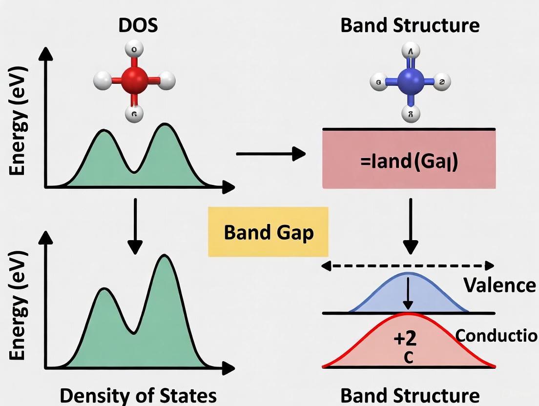
Band structure visualization employs two complementary representations: traditional band structure plots (energy versus wave vector k) and density of states (DOS) diagrams (state density versus energy). While band structure plots preserve momentum information essential for understanding carrier transport and optical transition selection rules, DOS diagrams provide a compressed view that quantifies how many electronic states exist at each energy level, making them particularly valuable for quick assessments of conductivity and band gaps [2]. This distinction becomes particularly significant in research comparing DOS and band structure plot analyses, where the choice of representation can emphasize different physical properties and applications.
Fundamental Principles of Band Gaps
Band Gap Definition and Classification
The band gap represents the minimum energy required to excite an electron from the valence band to the conduction band, thereby creating a charge carrier pair (electron and hole) that can participate in electrical conduction [1]. This energy difference fundamentally determines a material's electrical characteristics:
- Insulators feature large band gaps (typically >4 eV), making thermal or electrical excitation of electrons practically impossible at room temperature [1].
- Semiconductors possess intermediate band gaps (typically 0.1-4 eV), allowing modest thermal or optical excitation to generate significant numbers of charge carriers [1].
- Conductors exhibit zero or minimal band gaps due to overlapping valence and conduction bands, enabling free electron movement even without external excitation [1].
Table 1: Band Gap Classification of Materials
| Material Type | Band Gap Range (eV) | Electrical Conductivity | Example Materials |
|---|---|---|---|
| Conductor | 0 (no gap) | Very high | Copper, Silver, Gold |
| Semiconductor | 0.1 - 4.0 | Temperature dependent | Silicon, Germanium, GaAs |
| Insulator | >4.0 | Negligible | Diamond, SiO₂, AlN |
The band gap is not a fixed property but varies with temperature and pressure. With increasing temperature, lattice vibrations intensify, leading to larger interatomic spacing that typically decreases the band gap energy according to Varshni's empirical relationship [1]:
$$Eg(T) = Eg(0) - \frac{\alpha T^2}{T + \beta}$$
where $E_g(0)$ is the band gap at absolute zero, T is temperature, and α and β are material-specific constants. Similarly, external pressure modifies interatomic distances and bonding interactions, thereby altering the electronic structure and band gap characteristics [1].
Direct and Indirect Band Gaps
A crucial distinction in semiconductor physics separates materials based on whether they possess direct or indirect band gaps, which profoundly influences their optical and electronic behavior [1]. This classification depends on the alignment of the conduction band minimum and valence band maximum within the momentum space (k-space):
Direct Band Gap: The lowest energy state in the conduction band and the highest energy state in the valence band occur at the same k-vector value [1]. In these materials, electrons can transition directly between valence and conduction bands by emitting or absorbing a photon without requiring a change in momentum.
Indirect Band Gap: The conduction band minimum and valence band maximum occur at different k-vector values [1]. Electronic transitions between these extrema must involve both a photon and a phonon (lattice vibration) to conserve momentum, making these transitions statistically less probable.
Table 2: Direct vs. Indirect Band Gap Semiconductors
| Property | Direct Band Gap | Indirect Band Gap |
|---|---|---|
| k-vector alignment | Valence band maximum and conduction band minimum at same k | Valence band maximum and conduction band minimum at different k |
| Optical transitions | Direct photon absorption/emission | Requires photon and phonon |
| Transition probability | High | Lower |
| Light emission efficiency | Excellent | Poor |
| Typical applications | LEDs, laser diodes, solar cells | Transistors, digital electronics |
| Examples | GaAs, InP, CdTe | Silicon, Germanium, Diamond |
This direct/indirect band gap distinction has profound practical implications. Direct band gap materials demonstrate strong light-matter interactions with high absorption coefficients and efficient radiative recombination, making them ideal for optoelectronic applications including light-emitting diodes (LEDs), laser diodes, and high-efficiency photovoltaic cells [1]. Indirect band gap materials, despite their less efficient optical properties, remain technologically crucial, particularly silicon, which dominates microelectronics and solar cell manufacturing due to its abundance, stability, and excellent electrical properties.
Density of States (DOS) vs. Band Structure Plots
Band Structure Plots: Momentum-Resolved Electronic Structure
Band structure diagrams represent the relationship between electron energy (E) and wave vector (k) within the Brillouin zone of a crystalline material [2]. These plots preserve critical momentum-space information, including:
- Band dispersion revealing carrier effective masses through curvature
- Direct vs. indirect band gap identification through k-space alignment of band extrema
- Carrier mobility indications through band flatness/steepness
- Symmetry properties and degeneracies at high-symmetry points
The wave vector k relates to electron momentum in the crystal lattice, with each point along the band structure curves representing an allowed electronic state with specific (k, E) values [2]. Traditional band structure plots are essential for understanding phenomena sensitive to momentum conservation, including carrier transport properties, optical transition selection rules, and phonon interactions.
Density of States (DOS) Diagrams: Energy-Resolved State Distribution
The Density of States (DOS) provides a complementary representation by quantifying the number of available electronic states within a specific energy interval (ΔE), normalized by that interval, and plotted as a function of energy [2]. Essentially, DOS describes how many electronic states are "packed" at each energy level, integrating over all k-space information. DOS acts as a "compressed" version of the band structure, preserving key information including allowed/forbidden energy ranges and Fermi level position while discarding momentum-specific details [2].
Projected Density of States (PDOS) extends this concept by decomposing the total DOS into contributions from specific atoms, atomic orbitals (s, p, d, f), or chemical species [2]. This powerful technique enables researchers to identify which atomic components dominate particular energy regions, making it indispensable for understanding doping effects, chemical bonding, and catalytic mechanisms.
Table 3: Band Structure Plots vs. Density of States (DOS)
| Characteristic | Band Structure Plot | Density of States (DOS) |
|---|---|---|
| Horizontal axis | Wave vector (k) | Energy (E) |
| Vertical axis | Energy (E) | Number of states per unit energy |
| Information preserved | k-space details, band curvature, direct/indirect gap identification | State density, band gaps, Fermi level position |
| Information lost | State density distribution | Momentum-specific details |
| Primary applications | Carrier transport, optical transition rules, phonon interactions | Quick conductivity assessment, doping analysis, bonding studies |
| Computational cost | Higher (requires full Brillouin zone sampling) | Lower (energy integration) |
Research Implications: DOS-Band Structure Comparative Analysis
The distinction between DOS and band structure representations forms a critical methodological consideration in electronic structure research. While DOS diagrams provide a simplified, intuitive picture of state distribution that facilitates rapid material classification and property prediction, this convenience comes at the cost of lost momentum-resolution [2]. This information loss becomes particularly significant when investigating:
- Anisotropic materials whose electronic properties vary dramatically with crystallographic direction
- Direct vs. indirect band gap determination essential for optoelectronic applications
- Carrier effective mass calculations derived from band curvature
- Hot carrier dynamics and intervalley scattering processes
Research focused on the differences between DOS and band structure plot analyses must therefore carefully select the appropriate representation based on the specific physical phenomena under investigation. For property screening and rapid conductivity assessment, DOS provides superior efficiency, while for understanding fundamental electronic transitions and transport mechanisms, full band structure analysis remains indispensable [2].
Experimental and Computational Methodologies
Computational Approaches for Band Structure Determination
Density Functional Theory (DFT) represents the cornerstone computational methodology for predicting electronic band structures and DOS profiles [3]. Modern DFT implementations employ sophisticated exchange-correlation functionals to balance computational efficiency with accuracy:
- Generalized Gradient Approximation (GGA): Often using the Perdew-Burke-Ernzerhof (PBE) functional, GGA provides reasonable structural parameters and electronic properties at moderate computational cost [3].
- Hybrid Functionals (HSE06): Incorporating a portion of exact Hartree-Fock exchange, hybrid functionals yield significantly improved band gap accuracy, closely matching experimental values [3].
- Modified Becke-Johnson (mBJ) potential: This semi-local exchange potential provides band gap accuracy approaching hybrid functionals while maintaining computational efficiency similar to standard DFT [4].
- GW Approximation: Based on many-body perturbation theory, GW calculations deliver highly accurate quasiparticle band structures but require substantially greater computational resources.
Table 4: Computational Methods for Electronic Structure Calculation
| Method | Band Gap Accuracy | Computational Cost | Typical Applications |
|---|---|---|---|
| GGA-PBE | Underestimated | Low | Structural optimization, initial screening |
| HSE06 | High | High | Accurate band gap prediction, optoelectronic properties |
| mBJ | High | Medium | Band gap tuning studies, large systems |
| GW | Very High | Very High | Benchmark calculations, spectroscopic comparisons |
For layered materials like GeSe, DFT calculations reveal pronounced thickness-dependent electronic properties. Bulk GeSe exhibits a quasi-direct bandgap of approximately 1.414 eV using HSE06 functionals, while monolayer GeSe shows a substantially wider bandgap of 2.081 eV due to quantum confinement effects [3]. Such computational studies provide critical insights for designing tailored nanomaterials with optimized electronic and optical characteristics.
Experimental Validation Techniques
Theoretical band structure predictions require experimental validation through sophisticated spectroscopic techniques:
- Photoemission Spectroscopy: Angle-Resolved Photoemission Spectroscopy (ARPES) directly measures the electronic band structure by detecting the kinetic energy and emission angles of photoelectrons, providing both energy and momentum resolution.
- Optical Spectroscopy: Absorption, reflectance, and photoluminescence measurements determine the optical band gap and identify direct vs. indirect transition characteristics through analysis of absorption edges and excitation spectra.
- Scanning Tunneling Spectroscopy (STS): This technique probes local electronic density of states with atomic-scale spatial resolution, enabling direct measurement of band gaps and defect states.
- Electron Energy Loss Spectroscopy (EELS): By measuring energy losses of transmitted electrons, EELS provides information about band gaps, plasmon excitations, and interband transitions.
For the Cu₂NiXS₄ (X=Sn, Ge, Si) system, combined experimental and theoretical approaches demonstrate how band gap tuning through elemental substitution enables optimization for specific solar energy applications [4]. Similarly, comprehensive DFT studies of GeSe polymorphs reveal how computational predictions guide experimental synthesis toward materials with desired electronic characteristics [3].
Research Reagent Solutions and Computational Tools
Electronic band structure research employs specialized computational tools and methodological approaches that function as essential "research reagents" in theoretical and computational materials science:
- DFT Software Packages: CASTEP, VASP, Quantum ESPRESSO, and ABINIT provide robust platforms for first-principles electronic structure calculations, employing various exchange-correlation functionals to balance accuracy and computational efficiency [3].
- Electronic Structure Analysis Tools: Applications such as VESTA, VASPKIT, and p4vasp facilitate the visualization and interpretation of complex band structure and DOS data, enabling researchers to extract meaningful physical insights from raw computational output [2].
- Hybrid Functional Implementations: HSE06 functional implementations deliver improved band gap accuracy compared to standard GGA approximations, though at significantly increased computational cost [3].
- Van der Waals Corrections: For layered materials, dispersion-corrected functionals like DFT-D3(BJ) provide more accurate descriptions of interlayer interactions than standard GGA calculations [3].
- Post-Processing Algorithms: Band structure unfolding, Fermi surface calculation, and effective mass analysis tools enable deeper analysis of electronic properties beyond standard band structure plots.
- Spectral Decomposition Tools: Projected DOS (PDOS) and orbital-projected band structure algorithms facilitate the identification of specific atomic contributions to electronic states, crucial for understanding doping effects and chemical bonding [2].
- High-Performance Computing Resources: Parallel computing architectures, GPU acceleration, and optimized mathematical libraries enable computationally demanding simulations of complex material systems with thousands of atoms.
These computational "reagents" form the essential toolkit for modern electronic structure research, enabling predictive materials design and fundamental understanding of electronic properties across diverse material classes from traditional semiconductors to novel two-dimensional materials.
Electronic band structures form the fundamental theoretical framework for understanding and predicting the electrical and optical properties of materials. The distinction between direct and indirect band gaps represents a critical classification with profound implications for optoelectronic device applications, determining the efficiency of light-matter interactions in semiconductors. Similarly, the complementary representations offered by band structure plots and density of states diagrams provide researchers with versatile tools for analyzing different aspects of electronic behavior, from momentum-resolved carrier dynamics to energy-resolved state distributions.
Ongoing research into the differences between DOS and band structure plot analyses continues to refine our understanding of their respective strengths and limitations, guiding appropriate methodological selection for specific research questions. As computational methodologies advance with more accurate exchange-correlation functionals and efficient algorithms, and experimental techniques achieve higher energy and spatial resolution, our ability to precisely characterize and manipulate electronic band structures continues to expand. This progress underpins the development of next-generation electronic, photonic, and energy conversion devices through rational band gap engineering and material design.
The Density of States (DOS), denoted as g(E) or D(E), is a fundamental concept in condensed matter physics that describes the number of available electron states per unit volume per unit energy range in a material [5]. It provides a powerful summary of the electronic structure and plays a crucial role in determining a material's electrical, optical, and thermal properties. In the context of band gap research, the DOS offers complementary information to traditional band structure plots by quantifying how many states are available at each energy level, rather than merely showing which energy levels are permitted [6] [7]. While band structure plots depict the relationship between energy (E) and wave vector (k) along high-symmetry directions in the Brillouin zone, the DOS represents a projection of this information onto the energy axis, effectively integrating over all k-points [5] [7]. This integration makes the DOS particularly valuable for understanding the overall electronic behavior of materials, especially when investigating phenomena that depend on the total availability of states rather than their momentum-dependent characteristics.
The physical significance of the DOS becomes especially apparent when studying band gaps—ranges of energy that electrons cannot occupy in a material [7]. In the DOS profile, band gaps manifest as energy regions where g(E) = 0, indicating no available electronic states [7]. The shape and magnitude of the DOS near the band edges profoundly influence key material properties including electrical conductivity, optical absorption coefficients, and carrier effective masses [6]. For researchers investigating band gap differences between various materials, the DOS provides critical insights that complement band structure analysis, particularly through its revelation of Van Hove singularities—characteristic features in the DOS that arise from critical points in the band structure where the gradient vanishes [6]. These singularities often correspond to energies where the electronic properties undergo significant changes, making them valuable indicators for understanding material behavior.
Mathematical Definition and Fundamental Formulations
Core Mathematical Definition
The Density of States is formally defined through a fundamental relationship that connects the number of available states to energy. For a system with countable energy levels, the DOS per unit volume is expressed as:
D(E) = (1/V) × Σ δ(E - E(kᵢ)) [5]
where V represents the volume of the system, δ is the Dirac delta function, E(kᵢ) denotes the energy corresponding to wave vector kᵢ, and the summation extends over all states i. In the limit of a large system, where the wave vectors become quasi-continuous, this discrete sum transitions to an integral form:
D(E) = ∫ᵡ [dᵈk/(2π)ᵈ] × δ(E - E(k)) [5]
Here, d represents the dimensionality of the system (1, 2, or 3), and the integration occurs over the entire d-dimensional k-space [5]. This formulation highlights that the DOS essentially represents the volume in k-space between two constant energy surfaces separated by a differential energy difference dE. An alternative but equivalent definition relates the DOS to the derivative of the microcanonical partition function Zₘ(E):
D(E) = (1/V) × dZₘ(E)/dE [5]
This relationship connects the DOS to fundamental statistical mechanics, emphasizing its role in determining how many new states become accessible when the energy increases incrementally.
Dimensionality Effects on DOS Formulations
The mathematical expression for the DOS depends critically on the system's dimensionality, leading to distinct energy dependencies that profoundly influence physical properties:
Table: Density of States Formulas Across Different Dimensionalities
| Dimensionality | DOS Formula | Energy Dependence | Key Characteristics |
|---|---|---|---|
| 3D Systems | D₃D(E) = (m/(2π²ℏ³)) × (2mE)¹ᐟ² [5] | ∝ E¹ᐟ² | Continuous, parabolic dependence near band edges |
| 2D Systems | D₂D = m/(2πℏ²) [5] | Constant | Energy-independent for parabolic bands |
| 1D Systems | D₁D(E) = 1/(2πℏ) × (2m/E)¹ᐟ² [5] | ∝ E⁻¹ᐟ² | Diverges as E approaches zero |
The divergence observed in 1D systems gives rise to enhanced spectroscopic features and significantly influences electronic transitions [5]. These dimensional effects manifest clearly in the DOS profiles of low-dimensional structures such as quantum wells (2D), quantum wires (1D), and quantum dots (0D), where quantum confinement modifies the distribution of available states and consequently alters the material's optoelectronic properties.
Physical Significance and Interpretation of g(E)
Role in Determining Material Properties
The DOS function g(E) provides profound physical insights that extend far beyond a simple counting of available states. Its magnitude and energy dependence directly influence numerous material properties:
Electrical Conductivity: The DOS at the Fermi level (g(EF)) determines the number of electrons available to participate in electrical conduction [5] [7]. In metals, a high g(EF) correlates with strong conductivity, while in semiconductors and insulators, the magnitude of g(E) at the conduction and valence band edges governs the concentration of thermally activated charge carriers.
Optical Transitions: According to Fermi's Golden Rule, the rate of optical absorption depends on both the availability of initial states in the valence band and final states in the conduction band [7]. The joint density of states, which incorporates the DOS of both bands, directly influences absorption coefficients and determines the strength of optical transitions at different photon energies.
Thermal Properties: The electronic contribution to specific heat in solids is proportional to both g(EF) and temperature (Cₑₗ ∝ g(EF) × T) [5]. Materials with higher DOS values at the Fermi level consequently exhibit enhanced electronic heat capacities.
Phase Stability: The total electronic energy of a system depends on the integration of energy states weighted by the DOS and occupation probabilities. Variations in DOS distributions between different crystal structures can drive structural phase transitions.
Relationship to Band Structure and Band Gaps
The DOS serves as a critical bridge between abstract band structure concepts and measurable physical properties. While band structure plots depict the energy-momentum (E-k) relationship along specific crystallographic directions, the DOS represents the projection of these bands onto the energy axis, effectively integrating over all k-points in the Brillouin zone [7]. This relationship can be visualized through the following conceptual diagram:
The band gap manifests directly in the DOS as an energy region where g(E) = 0 [7]. The magnitude of the band gap corresponds to the energy span between the valence band maximum (where g(E) transitions from zero to finite values) and the conduction band minimum (where g(E) again becomes finite). Critical points in the band structure, known as Van Hove singularities, appear as distinctive features in the DOS where dE/dk = 0 [6]. These singularities often appear as sharp peaks or dips in the DOS and significantly influence optical absorption spectra and other electronic properties.
DOS in Different Dimensionalities and Material Systems
Dimensionality Effects on DOS Profiles
The dimensionality of a physical system profoundly influences the characteristics of its DOS, leading to fundamentally different electronic behavior:
Table: Characteristics of DOS Across Different Dimensionalities
| Dimension | System Examples | DOS Energy Dependence | Notable Features |
|---|---|---|---|
| 3D Systems | Bulk crystals, metals, conventional semiconductors [5] | D(E) ∝ E¹ᐟ² (parabolic) | Continuous, smoothly varying |
| 2D Systems | Quantum wells, graphene, 2D electron gases [5] | Constant (for ideal 2D) | Step-like function, energy-independent |
| 1D Systems | Carbon nanotubes, quantum wires, nanorods [5] | D(E) ∝ E⁻¹ᐟ² | Divergent at band edges |
| 0D Systems | Quantum dots, nanoparticles, molecules [7] | Discrete delta functions | No continuous energy bands |
In three-dimensional bulk materials, the DOS exhibits a continuous, parabolic energy dependence near the band edges for systems with parabolic energy dispersion [5]. This continuous distribution leads to predictable and well-understood electronic properties that form the basis of conventional semiconductor physics. In contrast, two-dimensional systems like graphene exhibit a markedly different DOS profile, including a linear energy dependence in the case of Dirac materials, which leads to unique electronic properties including high carrier mobility and unusual quantum Hall effects.
The progression toward lower dimensionality brings increasingly singular behavior in the DOS. One-dimensional systems display divergence at the band edges (D(E) ∝ E⁻¹ᐟ²) [5], which enhances electron correlation effects and can lead to exotic phenomena such as Luttinger liquid behavior, departing dramatically from conventional Fermi liquid theory. In zero-dimensional quantum dots and molecules, the DOS collapses entirely into discrete delta functions, reflecting the complete quantization of available states [7]. These dimensional effects highlight how nanostructuring and dimensional confinement can engineer DOS profiles to achieve desired electronic and optical properties.
Crystalline Symmetry and Anisotropic Materials
The symmetry of a crystalline system significantly impacts the computation and interpretation of DOS. In high-symmetry crystals such as those with face-centered cubic (FCC) or body-centered cubic (BCC) structures, the 48-fold or 24-fold symmetry of the Brillouin zone allows for substantial simplification of DOS calculations by reducing the computation to a small fraction of the zone [5]. However, in anisotropic materials or systems with lower symmetry, the DOS becomes strongly dependent on crystallographic direction, necessitating more sophisticated analysis approaches.
For anisotropic crystals, the projected density of states (PDOS) becomes an invaluable tool, decomposing the total DOS into contributions from specific atoms, orbitals, or crystallographic directions [5] [8]. This decomposition enables researchers to identify which atomic species and orbitals contribute most significantly to particular energy ranges, facilitating the design of materials with tailored electronic properties. For example, in metal-organic frameworks (MOFs), PDOS analysis can reveal whether the valence band maximum originates primarily from metal centers or organic linkers, information crucial for understanding and optimizing photocatalytic performance [9].
Experimental and Computational Methodologies
Computational Approaches for DOS Determination
Density Functional Theory (DFT) Calculations
Density Functional Theory has emerged as the predominant computational method for calculating electronic DOS from first principles. Modern DFT codes such as the Vienna Ab initio Simulation Package (VASP) enable precise determination of both total DOS (TDOS) and partial DOS (PDOS) [8]. A typical computational workflow involves:
Structural Optimization: Geometry optimization of the crystal structure to minimize total energy and determine the equilibrium lattice parameters.
Self-Consistent Field (SCF) Calculation: Iterative solution of the Kohn-Sham equations to determine the ground-state electron density.
Non-SCF Calculation: Calculation of the band structure and DOS on a dense k-point grid, typically with enhanced precision compared to the SCF calculation.
PDOS Analysis: Projection of the wavefunctions onto atomic orbitals to determine individual contributions from different atoms and orbital types.
For accurate DOS calculations, particularly those aimed at capturing fine features like Van Hove singularities, several critical parameters must be carefully considered [6]:
k-point Sampling: A sufficiently dense k-point mesh is essential for converging the DOS, particularly near critical points where small sampling can miss important features.
Energy Cutoff: The plane-wave energy cutoff must be high enough to accurately represent the wavefunctions without introducing unphysical oscillations in the DOS.
Exchange-Correlation Functional: The choice of functional (LDA, GGA, hybrid) significantly impacts the predicted band gap and detailed DOS structure.
DFT calculations have been successfully employed to study doping effects on DOS profiles, as demonstrated in research on Tl-doped α-Al₂O₃, where impurity introduction created new states within the original band gap, reducing its magnitude from the pure material's large band gap to approximately 2.38 eV [8].
Tight-Binding and Empirical Methods
While DFT provides first-principles accuracy, computationally efficient methods like tight-binding remain valuable for preliminary studies and large systems where DFT becomes prohibitively expensive. These semi-empirical approaches parameterize the Hamiltonian matrix elements based on experimental data or higher-level calculations, enabling rapid DOS estimation for systems containing thousands of atoms.
Experimental Probes of DOS
Several experimental techniques provide direct or indirect measurements of the DOS in materials:
Photoemission Spectroscopy: Both X-ray (XPS) and ultraviolet (UPS) photoemission spectroscopy directly probe the occupied DOS by measuring the kinetic energy of electrons ejected from the sample by photon irradiation [9]. Angle-resolved photoemission spectroscopy (ARPES) additionally provides momentum resolution, enabling direct comparison with band structure calculations.
Inverse Photoemission Spectroscopy (IPES): This technique complements photoemission by probing the unoccupied DOS above the Fermi level [9].
Scanning Tunneling Spectroscopy (STS): By measuring the differential conductance (dI/dV) in scanning tunneling microscopy, STS provides a direct measure of the local DOS (LDOS) with atomic-scale spatial resolution.
Optical Spectroscopy: Techniques such as UV-Vis absorption spectroscopy and spectroscopic ellipsometry provide indirect information about the DOS through the optical absorption spectrum, particularly near the band edges [9] [8]. The Tauc plot method is commonly used to extract optical band gaps from absorption data, though accurate interpretation requires careful consideration of whether transitions are direct or indirect [9].
The following diagram illustrates the integrated computational and experimental workflow for DOS analysis:
Table: Essential Computational Tools for DOS Analysis
| Tool Name | Type/Methodology | Primary Function in DOS Analysis | Key Features |
|---|---|---|---|
| VASP [8] | DFT Package | First-principles DOS calculation | Projector augmented-wave method, hybrid functionals, spectral properties |
| Quantum ESPRESSO | DFT Package | Ab initio DOS computation | Plane-wave basis set, pseudopotentials, open-source |
| WIEN2k | DFT Package | Full-potential DOS calculations | Linearized augmented plane-wave method, high accuracy |
| VESTA | Visualization Software | Crystal structure and charge density visualization | Integration with electronic structure codes, volumetric data rendering |
Experimental Techniques for DOS Validation
Table: Experimental Methods for DOS Characterization
| Technique | Physical Principle | DOS Information Obtained | Key Limitations |
|---|---|---|---|
| XPS/UPS [9] | Photoelectric effect | Occupied DOS with elemental specificity | Surface-sensitive, ultra-high vacuum required |
| IPES [9] | Inverse photoemission | Unoccupied DOS above E_F | Lower energy resolution than photoemission |
| STM/STS | Quantum tunneling | Local DOS with atomic resolution | Conducting samples only, complex interpretation |
| UV-Vis Spectroscopy [9] [8] | Optical absorption | Joint DOS between valence and conduction bands | Indirect probe, requires modeling for DOS extraction |
Advanced Concepts and Research Applications
Van Hove Singularities and Their Implications
Van Hove singularities represent critical points in the band structure where the gradient vanishes (∇ₖE(k) = 0), leading to distinctive features in the DOS [6]. These singularities manifest as sharp peaks, dips, or discontinuities in the DOS and profoundly influence a material's optical and electronic properties. In one-dimensional systems, these singularities exhibit the characteristic D(E) ∝ E⁻¹ᐟ² divergence [5], while in two-dimensional systems, they typically appear as logarithmic singularities. Three-dimensional systems generally display weaker discontinuities in the derivative of the DOS at Van Hove singularities.
The presence of Van Hove singularities near the Fermi level can dramatically enhance electronic phenomena, including:
Superconductivity: Enhanced DOS at E_F increases electron-phonon coupling, potentially elevating superconducting transition temperatures.
Magnetic Instabilities: High DOS at the Fermi level can promote Stoner ferromagnetism or other magnetic ordering.
Optical Transitions: Sharp features in the joint DOS at specific energies lead to strong optical absorption peaks.
Recent research on twisted bilayer graphene has highlighted the role of Van Hove singularities in producing correlated insulating states and unconventional superconductivity, demonstrating how modern materials design can strategically position these singularities to engineer novel quantum phenomena.
Band Gap Engineering Through DOS Modification
Strategic modification of the DOS represents a powerful approach to band gap engineering, with significant implications for electronic and optoelectronic applications. Several methodologies enable controlled alteration of DOS profiles:
Doping and Alloying: Introduction of impurity atoms can create new states within the band gap, effectively reducing its magnitude [8]. As demonstrated in Tl-doped α-Al₂O₃, foreign atoms introduce defect states that hybridize with the host material's bands, modifying both the band gap and the overall DOS shape [8].
Dimensional Confinement: Reducing system dimensionality from 3D to 2D, 1D, or 0D dramatically alters the DOS profile, typically increasing band gaps due to quantum confinement effects while introducing characteristic dimensional signatures [5].
Strain Engineering: Application of mechanical strain modifies the band structure by altering bond lengths and symmetry, consequently reshaping the DOS and potentially inducing metal-insulator transitions.
Heterostructure Design: Combining different materials in heterostructures or superlattices creates modified DOS profiles through interfacial interactions and quantum confinement, enabling properties not available in single-phase materials.
For photocatalyst applications, as explored in Metal-Organic Frameworks (MOFs), precise knowledge of both the band gap and the DOS profile near the band edges is essential for optimizing light absorption and charge carrier separation [9]. The distinction between direct and indirect band gaps, discernible through careful DOS analysis, critically influences recombination kinetics and photocatalytic efficiency [9].
The Density of States g(E) represents far more than a simple counting of available electron states—it provides a fundamental connection between a material's electronic structure and its macroscopic physical properties. Through its energy-dependent distribution, the DOS reveals critical information about band gaps, Van Hove singularities, effective masses, and dimensionality effects that collectively determine electrical, optical, and thermal behavior [5] [6]. In band gap research, the DOS complements traditional band structure plots by projecting the complex E-k relationship onto the energy axis, highlighting features that might be obscured in conventional band structure representations [7].
Modern computational approaches, particularly Density Functional Theory, enable precise calculation of both total and partial DOS, facilitating material design with tailored electronic properties [8]. These theoretical predictions are validated through sophisticated experimental techniques including photoemission spectroscopy, scanning tunneling spectroscopy, and optical methods [9]. As materials research increasingly focuses on low-dimensional systems and complex heterostructures, the DOS continues to provide essential insights for understanding and engineering quantum phenomena, making it an indispensable tool in condensed matter physics and materials science.
In the computational and theoretical study of condensed matter physics, the electronic band gap is a defining property that determines whether a material is a metal, semiconductor, or insulator. Researchers typically probe this property through two primary, complementary representations: the electronic band structure plot, which displays the energy of electron states as a function of their crystal momentum (( \mathbf{k} )), and the Density of States (DOS) plot, which shows the number of available electron states per unit energy. Within the context of a broader thesis on band gap differences between these representations, this whitepaper establishes the ideal theoretical scenario for their perfect alignment. Understanding this foundational relationship is crucial for diagnosing computational inaccuracies, selecting appropriate methodologies, and correctly interpreting electronic structure calculations in materials design and development.
The central thesis of this work is that in an ideal, perfectly converged calculation for an infinite, pristine crystal, the fundamental band gap must be identical in both the band structure and the DOS. Any discrepancy between them is not a theoretical feature but an artifact of numerical approximation or methodological limitation. This guide details the theoretical underpinnings of this alignment, provides protocols for its achievement, and offers a toolkit for researchers to validate their own calculations.
Theoretical Foundations of Band Gaps and DOS
Electronic Band Structure
In solid-state physics, the electronic band structure describes the range of energy levels that electrons may occupy within a solid. It is derived by solving the Schrödinger equation for an electron in a periodic potential, leading to Bloch waves as solutions. The resulting dispersion relations, ( E_n(\mathbf{k}) ), show how the energy of an electron in band ( n ) varies with its wave vector, ( \mathbf{k} ), within the Brillouin zone [7].
A band gap is a forbidden range of energies that electrons cannot possess. It separates the valence band (the highest range of electron energies occupied at absolute zero) from the conduction band (the lowest range of unoccupied energies) [7]. Band gaps are categorized as:
- Direct band gap: The minimum energy difference between the conduction band minimum (CBM) and valence band maximum (VBM) occurs at the same ( \mathbf{k} )-point.
- Indirect band gap: The CBM and VBM are located at different ( \mathbf{k} )-points [7].
Density of States (DOS)
The Density of States, ( g(E) ), is a fundamental quantity defined as the number of electronic states per unit volume per unit energy. Formally, it is calculated by integrating over the Brillouin zone [5]: [ g(E) = \int_{\text{BZ}} \frac{d^d k}{(2\pi)^d} \cdot \delta(E - E(\mathbf{k})) ] where ( d ) is the dimensionality of the system. This integral effectively counts all the ( \mathbf{k} )-points in the Brillouin zone that have an energy between ( E ) and ( E + dE ) [5].
A key theoretical consequence is that in an energy range where no electronic states exist—that is, within a band gap—the DOS must be zero. Therefore, the fundamental band gap appears in the DOS plot as an energy region where the DOS drops to zero, bounded by the valence band edge on the low-energy side and the conduction band edge on the high-energy side [7] [5].
The Ideal Theoretical Alignment
The fundamental band gap, ( Eg ), is defined as: [ Eg = E{\text{CBM}} - E{\text{VBM}} ] where ( E{\text{CBM}} ) is the energy of the conduction band minimum and ( E{\text{VBM}} ) is the energy of the valence band maximum.
In the ideal scenario, this single value of ( E_g ) must be reflected consistently in both representations:
- In the band structure plot, ( E_g ) is the direct visual difference in energy between the lowest point of the conduction band and the highest point of the valence band across all ( \mathbf{k} )-points.
- In the DOS plot, ( E_g ) is the width of the energy region where the DOS is identically zero.
The following conceptual diagram illustrates this ideal, self-consistent relationship.
Methodological Protocols for Achieving Ideal Alignment
Achieving the ideal alignment in practical computations requires careful attention to numerical parameters. The following workflow and protocols ensure self-consistent results.
Computational Workflow for Consistent Band Gap Calculation
Detailed Experimental and Computational Protocols
Protocol 1: Ground-State Calculation for Self-Consistent Charges
- Objective: To obtain a converged electron density for the crystal structure.
- Method: Perform a self-consistent field (SCF) calculation using a plane-wave basis set as implemented in codes like Quantum ESPRESSO or VASP [10] [11].
- Key Parameters:
- K-point sampling: A Monkhorst-Pack grid must be used. Convergence must be tested by increasing the grid density (e.g., from (4\times4\times4) to (8\times8\times8)) until the total energy change is below 1 meV/atom [11].
- Energy cutoff: The plane-wave kinetic energy cutoff must be tested for convergence.
- Convergence threshold: The SCF cycle should be run until the energy change between iterations is below (10^{-5}) eV or similar stringent criteria [11].
- Output: The self-consistent charge density and wavefunctions, which serve as the fixed input for the subsequent non-SCF band structure and DOS calculations.
Protocol 2: Band Structure Calculation
- Objective: To compute the electronic energies along a high-symmetry path in the Brillouin zone.
- Method: A non-SCF calculation is performed using the fixed charge density from Protocol 1.
- Key Parameters:
- K-point path: The calculation uses a string of high-symmetry points (e.g., Γ, X, L, W) in the Brillouin zone, typically with 20-50 points between each high-symmetry point [11].
- Band gap extraction: The band gap ( E_g^{BS} ) is identified as the difference between the lowest CBM and the highest VBM across the entire calculated path.
Protocol 3: Density of States Calculation
- Objective: To compute the number of electronic states as a function of energy.
- Method: A non-SCF calculation is performed using the same fixed charge density from Protocol 1.
- Key Parameters:
- K-point grid: A dense, uniform Monkhorst-Pack grid is critical. This grid must be significantly denser than the one used for the SCF calculation to ensure a smooth and accurate DOS. Convergence should be tested until the DOS in the band gap region is numerically zero and the band edges are sharp [11].
- Smearing: A small Gaussian or tetrahedron smearing width (e.g., 0.01-0.05 eV) is applied to approximate a continuous function from the discrete K-point sampling.
- Band gap extraction: The band gap ( E_g^{DOS} ) is identified as the energy range where the DOS is zero. The VBM and CBM are taken as the energies where the DOS becomes non-zero.
The Scientist's Toolkit: Essential Computational Reagents
Table 1: Key Computational Tools and Parameters for Band Structure Analysis
| Research Reagent / Tool | Function / Role in Calculation | Critical Parameters & Notes |
|---|---|---|
| DFT Code (e.g., VASP, Quantum ESPRESSO, WIEN2k) | Performs the core electronic structure calculation by solving the Kohn-Sham equations. | Choice of exchange-correlation functional (e.g., PBE, HSE06, mBJ) is the primary source of band gap accuracy [10] [12]. |
| K-point Grid (SCF) | Samples the Brillouin zone to achieve a converged electron density and total energy. | Must be sufficiently dense; convergence is system-dependent. A sparse grid leads to inaccurate charges [11]. |
| K-point Path (Band Structure) | Defines the trajectory in k-space for plotting the band dispersion. | Must connect high-symmetry points (e.g., Γ-X-W-K-Γ) to reveal the true VBM and CBM [7] [11]. |
| Dense K-point Grid (DOS) | Integrates over the entire Brillouin zone to count available states at each energy. | Must be extremely dense to avoid spurious gaps or peaks; typically denser than the SCF grid [11]. |
| Pseudopotential / PAW Dataset | Represents the core electrons and nucleus, reducing computational cost. | Influences the accuracy of valence electron description. Norm-conserving or PAW potentials are standard [10]. |
| Post-Processing Tool (e.g., dp_dos, BoltzTraP) | Processes raw eigenvalue data to generate DOS/PDOS plots and other properties. | Smearing parameter must be chosen carefully to balance smoothness and artificial band gap narrowing [11]. |
Quantitative Benchmarking and Data Presentation
A critical step in validating the ideal scenario is the quantitative comparison of results obtained from different computational methods. The following tables summarize benchmark data.
Table 2: Comparison of Band Gaps (eV) Calculated with Different Methods for Selected Materials
| Material | Experimental Gap | LDA/GGA-PBE | HSE06 | mBJ | G₀W₀-PPA | QSGW | QSGŴ |
|---|---|---|---|---|---|---|---|
| Silicon | 1.17 (indirect) | ~0.6 [10] | ~1.3 [10] | ~1.2 | ~1.2 [10] | ~1.3 | ~1.2 |
| TiO₂ (Anatase) | 3.2 | ~2.1 | ~3.1 | ~3.3 | ~3.4 | ~3.5 | ~3.3 |
| Nb₃O₇(OH) | - | ~1.7 (GGA) [12] | - | 1.7 (TB-mBJ) [12] | - | - | - |
| Ta-doped Nb₃O₇(OH) | - | - | - | 1.266 (TB-mBJ) [12] | - | - | - |
| Sb-doped Nb₃�O₇(OH) | - | - | - | 1.203 (TB-mBJ) [12] | - | - | - |
Table 3: Convergence Parameters for a Typical DFT Calculation (e.g., Anatase TiO₂)
| Parameter | SCF Calculation | Band Structure | DOS Calculation |
|---|---|---|---|
| K-point Grid | (8\times8\times8) MP grid | Path: Z-Γ-X-P (20-45 pts/segment) [11] | (16\times16\times16) MP grid or denser [11] |
| Energy Cutoff | 500 eV | Same as SCF | Same as SCF |
| SCC Tolerance | (10^{-5}) eV [11] | Non-SCF | Non-SCF |
| Gaussian Smearing | - | - | 0.01 eV |
Discussion: Interpretation and Common Pitfalls
The relationship between flat regions in the band structure and peaks in the DOS is a key point of interpretation. A flat dispersion ( E_n(\mathbf{k}) ) over a large region of k-space implies a high density of states at that particular energy, resulting in a peak in the DOS [13]. Conversely, a strongly dispersive band contributes a smaller amount to the DOS over a wider energy range. This is why the DOS provides a complementary, integrated view of the electronic structure detailed in the band plot.
In a real calculation, several pitfalls can break the ideal alignment:
- Insufficient K-points for DOS: This is the most common error. A sparse k-grid fails to sample the Brillouin zone adequately, making the DOS appear to have a non-zero value in the band gap region, thus obscuring the true gap [11].
- Incorrect Band Structure Path: If the calculated k-path does not include the actual k-points where the VBM and CBM reside, the band structure plot will show an incorrectly large band gap.
- Methodological Limitations: Standard Density Functional Theory (DFT) with local or semi-local functionals (like LDA and GGA) is known to systematically underestimate band gaps [10] [8]. More advanced methods like hybrid functionals (HSE06) or many-body perturbation theory (the GW approximation) are required for quantitatively accurate gaps, but the principle of alignment between DOS and band structure still holds for any given method [10].
This whitepaper has established the fundamental principle that in an ideal theoretical scenario, the band gap must be perfectly aligned in the electronic band structure and Density of States plots. This alignment serves as a critical benchmark for the numerical quality of an electronic structure calculation. The provided protocols, workflows, and toolkit empower researchers to systematically achieve this self-consistency in their work. For a broader thesis on band gap discrepancies, this ideal case forms the essential baseline from which all deviations—whether arising from numerical artifacts, methodological errors, or the study of inherently disordered or defective systems—must be measured and understood. Adherence to the rigorous computational practices outlined herein is paramount for generating reliable, reproducible data that can confidently guide materials discovery and optimization.
In computational materials science, the electronic band gap is a paramount parameter, dictating whether a material is classified as a metal, semiconductor, or insulator, and subsequently determining its potential applications in electronic and optoelectronic devices [14] [15]. This property represents the minimum energy required to excite an electron from the valence band, where electrons are bound to atoms, to the conduction band, where electrons can move freely and conduct electricity [14]. While density functional theory (DFT) is a cornerstone method for calculating electronic structures, it is common to encounter differing values for a material's band gap depending on whether it is derived from a band structure plot or a Density of States (DOS) calculation [16]. These discrepancies are not merely numerical artifacts; they stem from fundamental methodological differences and have profound implications for the predictive classification of new materials and the reliable design of next-generation devices. This guide examines the origins of these discrepancies, their impact on material properties, and provides robust protocols for researchers to validate their computational results, a crucial framework for any thesis investigating band gap differences.
Fundamental Concepts: DOS and Band Structure
The electronic band structure of a crystal describes the range of energy levels that electrons may occupy, as well as the forbidden energy ranges known as band gaps [15]. It is typically plotted as electron energy versus the electron wavevector, k, along high-symmetry paths in the Brillouin zone [15]. The band structure provides a k-resolved view of the electronic levels, making it possible to identify the precise points where the valence band maximum (VBM) and conduction band minimum (CBM) occur.
In contrast, the Density of States (DOS) describes the number of electronic states available at each energy level, integrated over all k-points in the Brillouin zone [16]. It provides a global, k-integrated perspective of the electronic energy distribution. The band gap is identified from the DOS as an energy range where the density of available states is zero.
Table 1: Core Concepts of DOS and Band Structure
| Feature | Density of States (DOS) | Band Structure Plot |
|---|---|---|
| Fundamental Output | Number of electronic states per unit energy | Energy of electronic states as a function of wavevector, k |
| k-space Resolution | Integrated over the entire Brillouin zone | Resolved along specific high-symmetry paths |
| Primary Strength | Identifying overall electronic character and energy gaps | Revealing band dispersion and direct/indirect nature of gaps |
| Band Gap Identification | Energy range with zero density of states | Energy difference between the highest valence and lowest conduction bands |
Origins of Discrepancy Between DOS and Band Structure
A fundamental source of discrepancy between band gaps from DOS and band structure lies in their different k-space sampling. The DOS is typically calculated using a uniform, dense k-point grid over the entire Brillouin zone. The band structure, however, is computed along a specific set of high-symmetry lines connecting special k-points [16]. Consequently, the uniform k-point grid used for the DOS might not include the specific k-point where the CBM or VBM is located, and vice-versa [16].
For example, in silicon, the VBM is at the Γ-point (the center of the Brillouin zone), while the CBM is near the X-point [15]. A band structure calculation explicitly tracing the bands from Γ to X will capture this indirect gap. A DOS calculation will also capture it, provided the uniform k-mesh is sufficiently dense to sample the region near the X-point with high enough resolution. If the mesh is too coarse, the DOS might inaccurately represent the band edges, leading to an incorrect gap. This inherent difference in methodology means that "DOS data and line-mode band structure may not completely agree on all derived properties such as the band-gap due to k-point grid differences" [16].
Implications for Material Properties and Classification
Inaccurate band gap determination has direct and severe consequences for predicting material properties and correct classification.
Electrical Conductivity and Material Classification
The band gap is the primary property used to classify a material's electrical character. A zero band gap indicates a metal or semimetal, a small gap (typically < ~3-4 eV) indicates a semiconductor, and a large gap indicates an insulator [14] [17]. An underestimated band gap can lead to the misclassification of a semiconductor as a metal, or an insulator as a semiconductor. The Materials Project notes that "several known insulators are predicted to be metallic" by standard DFT functionals, highlighting the severity of this issue [16].
Optical Properties and Device Performance
The band gap directly determines the energy of photons a material can absorb or emit, which is critical for optoelectronic applications like solar cells, light-emitting diodes (LEDs), and lasers [17] [18]. Furthermore, the direct or indirect nature of the band gap, which can only be determined from the band structure plot, is crucial. In a direct band gap semiconductor, the CBM and VBM occur at the same k-point, allowing efficient light emission. In an indirect semiconductor, the CBM and VBM are at different k-points, making light emission much less likely as it requires a phonon (lattice vibration) to conserve momentum [15]. A material's potential for light-emitting devices is therefore heavily dependent on a correct interpretation of the band structure.
Experimental Protocols and Validation Methodologies
To ensure reliable results, researchers must adopt rigorous validation protocols. The following methodology, derived from the practices of the Materials Project, provides a robust framework for reconciling discrepancies.
Protocol 1: Recomputing Band Gap from DOS
This is often the most reliable method to verify a band gap value.
- Data Acquisition: Obtain the complete DOS data for the material of interest. This is typically available via materials databases (e.g., Materials Project API) or from the output of DFT codes like VASP.
- Identify Band Edges: Locate the CBM and VBM by finding the lowest energy at which the DOS becomes non-zero above the Fermi level and the highest energy at which the DOS is non-zero below the Fermi level.
- Calculate Gap: The band gap is computed as: ( E{\text{gap}} = E{\text{CBM}} - E_{\text{VBM}} ).
Table 2: Key Research Reagent Solutions for Electronic Structure Analysis
| Tool / Reagent | Function / Description | Application in Validation |
|---|---|---|
| DFT Code (e.g., VASP, Quantum ESPRESSO) | Performs first-principles electronic structure calculations. | Generates the fundamental DOS and band structure data. |
| pymatgen Library | A robust, open-source Python library for materials analysis. | Provides tools to parse calculation outputs and recompute properties like band gap from DOS. |
| Materials Project API | Programmable interface to a vast database of computed materials properties. | Allows fetching of pre-computed DOS and band structure data for validation and benchmarking. |
Protocol 2: Cross-Validation with Band Structure
This protocol checks for consistency between the DOS and the band structure plot.
- Acquire Band Structure: Obtain the calculated band structure object along high-symmetry paths.
- Correct Fermi Level Reference: In some cases, the band structure plot may have an incorrectly placed Fermi level. To correct this, use the VBM energy (( E_{\text{VBM}} )) obtained from the DOS calculation to reconstruct the band structure's energy reference.
- Recompute Gap from Corrected Bands: Calculate the band gap from the corrected band structure object, identifying the global CBM and VBM across all plotted k-points.
The workflow below illustrates the decision process for diagnosing and resolving a band gap discrepancy.
Advanced Considerations: DFT Limitations and Future Directions
It is critical to recognize that discrepancies can also arise from the inherent limitations of DFT itself. Standard exchange-correlation functionals (e.g., LDA, GGA) are known to severely underestimate band gaps, often by 50% or more, a problem distinct from the DOS/band structure sampling issue [16]. This error originates from approximations in the exchange-correlation functional and a derivative discontinuity in the true density functional [16].
More advanced methods, such as hybrid functionals (e.g., HSE06) or the GW approximation, can significantly improve accuracy but at a substantially higher computational cost [19] [16]. Furthermore, the rise of machine learning models trained on experimental properties offers a promising, low-cost alternative for initial band gap estimation, though they may not yet match the accuracy of dedicated quantum mechanical methods for novel materials [14].
Discrepancies between band gaps derived from DOS and band structure plots are a critical issue in computational materials science. They stem from fundamental differences in k-space sampling and can lead to the misclassification of materials and incorrect predictions of their electronic and optical properties. By understanding the origins of these discrepancies and employing the rigorous validation protocols outlined in this guide—specifically, recomputing the gap from the DOS and systematically cross-validating with the band structure—researchers can ensure the reliability of their computational predictions. As band gap engineering continues to drive innovation in technologies from photovoltaics to quantum computing, a meticulous approach to resolving these discrepancies is not just an academic exercise, but a necessary practice for the accurate design and discovery of new functional materials.
Computational Methods: Calculating Accurate Band Gaps with DFT and Beyond
In the context of researching band gap differences between Density of States (DOS) and band structure plots, understanding the underlying calculation workflows is paramount. The band structure of a material depicts the allowed energy states for electrons as a function of their crystal momentum vector k, while the DOS quantifies the number of available energy states per unit volume at a specific energy level [20] [5]. These two representations are fundamentally interconnected; the DOS is, in fact, mathematically derived from the band structure. The relationship is encapsulated by the formula for the DOS, D(E), which is an integral over the Brillouin zone in k-space, counting all states that have energy E [5]. Peaks in the DOS, known as van Hove singularities, correspond to regions in the band structure where the energy is flat over a large area of k-space, meaning many electron states share the same energy [13]. This foundational relationship is critical for explaining why the band gap measured from a band structure plot can sometimes differ from that observed in a DOS plot, a key focus of advanced materials research.
The Computational Workflow: From SCF to NSCF to DOS
The determination of electronic properties like band structure and DOS in modern computational materials science is typically a two-step process, utilizing Self-Consistent Field (SCF) and non-self-consistent field (nscf) calculations sequentially [21]. This workflow is essential for achieving accurate results with manageable computational effort. The following diagram illustrates the logical sequence and data flow between these different calculation types.
Self-Consistent Field (SCF) Calculation
The SCF calculation is the critical first step in determining the ground-state properties of a material. Its primary goal is to solve the Kohn-Sham equations, which are nonlinear differential equations, until the electron charge density and potential of the system no longer change significantly between iterations [21]. This is an iterative process where an initial guess for the charge density is used to construct the Kohn-Sham Hamiltonian. This Hamiltonian is then diagonalized to obtain electronic wavefunctions, which are used to compute a new charge density. This new density is mixed with the old one, and the process repeats until the system's total energy converges to within a pre-determined threshold [21]. The key outcome of a successful SCF calculation is a converged charge density, which represents the self-consistent ground state of the system. This calculation is typically performed on a uniform grid of k-points in the Brillouin zone that is sufficiently dense to ensure convergence of the total energy.
Non-Self-Consistent Field (NSCF) Calculation
Once the SCF calculation is complete and the converged charge density is obtained, the NSCF calculation is performed. The term "non-self-consistent" signifies that this step does not involve updating the charge density [21]. Instead, the NSCF calculation reads the pre-converged charge density from the SCF step and uses it to construct the Kohn-Sham Hamiltonian exactly once. This Hamiltonian is then diagonalized on a much denser grid of k-points [21]. This approach is computationally faster than a full SCF calculation with an equally dense k-grid because it avoids the expensive iterative cycle. The primary purpose of the NSCF step is to obtain a highly detailed sampling of the electronic eigenvalues (energies) over the Brillouin zone. This dense sampling is essential for producing smooth and accurate plots of the DOS and for tracing the electronic bands along specific high-symmetry paths for band structure plots [21].
Density of States (DOS) Calculation
The DOS is calculated directly from the results of the NSCF calculation. Using the densely sampled eigenvalues from the NSCF run, the DOS is computed by counting the number of electronic states at each energy level. The mathematical definition involves summing over all bands and k-points, often using a broadening function (like a Gaussian) to produce a continuous curve from the discrete energy levels [20]. The formula for the DOS per unit volume is: [ D(E) = \frac{1}{V} \sum{n, \mathbf{k}} \delta(E - En(\mathbf{k})) ] where ( E_n(\mathbf{k}) ) is the energy of band n at point k [5]. In practice, the delta function is approximated by a narrow Gaussian. The resulting DOS plot reveals the concentration of electronic states at specific energies, with peaks indicating high densities. The band gap is identified in the DOS as an energy region between the valence band (occupied states) and the conduction band (unoccupied states) where the DOS is zero [5].
Key Differences Between SCF and NSCF Calculations
The distinct roles of SCF and NSCF calculations lead to fundamental differences in their setup, execution, and purpose. These differences are summarized in the table below for easy comparison.
| Feature | SCF Calculation | NSCF Calculation |
|---|---|---|
| Primary Goal | Find the ground-state converged charge density and total energy [21]. | Obtain detailed eigenvalue spectrum on a dense k-point set for post-processing [21]. |
| Computational Process | Iterative and self-consistent until energy convergence is achieved [21]. | Single-shot diagonalization of the Hamiltonian without updating charge density [21]. |
| k-point Grid | Uses a uniform grid that is sufficiently dense for energy convergence [21]. | Uses a denser, targeted grid (uniform for DOS; path for band structure) [21]. |
| Output | Converged charge density, total energy, Fermi energy. | Detailed eigenvalues and eigenfunctions for all specified k-points. |
| Relative Speed | Slower due to the iterative process. | Faster for the same dense grid, as it avoids self-consistency [21]. |
| Downstream Use | Prerequisite for any subsequent property calculation. | Directly used for plotting DOS, band structure, and other spectral properties. |
Essential Computational Parameters and Protocols
To ensure reproducible and accurate results, particular attention must be paid to the configuration of SCF and NSCF calculations. The following table outlines the key parameters and their functions, constituting a "Scientist's Toolkit" for these computations.
| Item / Parameter | Function / Purpose |
|---|---|
| Plane-Wave Kinetic Energy Cutoff | Determines the basis set size. A higher cutoff increases computational cost but improves accuracy by better describing the wavefunctions. |
| SCF k-point Grid | A uniform mesh (e.g., 8x8x8) for sampling the Brillouin zone. Must be converged to ensure the total energy and charge density are accurate [21]. |
| SCF Energy Convergence Threshold | The criterion (e.g., 1e-6 Ry) for stopping the iterative cycle, ensuring the solution is self-consistent [21]. |
| NSCF k-point Grid (for DOS) | A much denser uniform grid (e.g., 24x24x24) to accurately compute the integral over the Brillouin zone for a smooth DOS [21]. |
| NSCF k-point Path (for Band Structure) | A high-symmetry path (e.g., Γ-X-L-Γ) connecting specific points in the Brillouin zone for plotting band dispersion. |
| Smearing Width | A small broadening parameter (e.g., 0.01 Ry) used to replace the delta function in the DOS calculation, yielding a continuous plot [20]. |
Detailed Methodology for a Standard DOS Workflow
- Structural Relaxation: Begin with a fully optimized crystal structure to ensure atomic positions and lattice constants are at their ground-state configuration.
- SCF Calculation:
- Input: Select a converged plane-wave cutoff energy and a k-point grid that yields a total energy converged to within a desired tolerance (e.g., 1 meV/atom).
- Protocol: Run the SCF calculation with a strict energy convergence threshold. The output to carefully monitor is the total energy, ensuring it stabilizes across iterations.
- Output: The crucial output file is the converged charge density data file.
- NSCF Calculation:
- Input: Use the converged charge density from the SCF step as the input. Set the calculation type to 'nscf'. Specify a k-point grid for the DOS that is significantly denser than the one used in the SCF step. For a band structure plot, instead of a uniform grid, specify a path along high-symmetry lines in the Brillouin zone.
- Protocol: This is a single-step calculation. The software will read the fixed charge density, construct the Hamiltonian, and diagonalize it for all the specified k-points.
- Output: The output is a file containing the eigenvalues (energy levels) for every band and every k-point specified.
- DOS and Band Structure Post-Processing:
- Use a dedicated post-processing tool (e.g.,
dos.xandbands.xin Quantum ESPRESSO) that reads the NSCF output. - For the DOS, the tool will sum over all k-points and bands, applying the chosen smearing to produce the final
D(E)versusEdata. - For the band structure, the tool will trace the eigenvalues along the high-symmetry path, generating data ready for plotting.
- Use a dedicated post-processing tool (e.g.,
Interpreting Results and Band Gap Analysis
A central challenge in the thesis context is reconciling band gaps observed in DOS plots versus band structure plots. The fundamental relationship between band structure and DOS provides the explanation. The DOS is a projection of the band structure onto the energy axis [5]. In a perfect crystal, the band gap should be identical in both representations. However, discrepancies can arise in practice. If the k-point grid in the NSCF calculation is not dense enough, the DOS might fail to capture shallow band extrema located at specific k-points, leading to an inaccurate band gap measurement from the DOS. Conversely, the band structure plot might clearly show the global minimum of the conduction band and the global maximum of the valence band, giving the true fundamental band gap. Therefore, a rigorous methodology requires verifying the convergence of the DOS-derived band gap with respect to the density of the NSCF k-point grid, using the band structure plot as a benchmark for the correct value. This workflow, from a converged SCF to a dense NSCF calculation, is designed precisely to minimize such discrepancies and ensure the reliability of the computed electronic properties.
In the realm of computational materials science, particularly in research focused on accurately determining electronic band gaps, the method of k-point sampling is a fundamental computational parameter that can significantly influence the outcome of density functional theory (DFT) calculations. The central challenge this article addresses is the frequent discrepancy observed between band gaps extracted from density of states (DOS) plots and those obtained directly from electronic band structure plots. This discrepancy often originates from an incomplete understanding of the distinct purposes and requirements for k-point sampling in these two types of analysis.
For DOS calculations, the objective is to achieve a high-density, uniform sampling across the entire Brillouin Zone (BZ) to accurately integrate electronic states for a precise representation of state distribution over energy [11] [22]. In contrast, band structure calculations trace the energy levels of electronic states along specific, high-symmetry paths between critical points in the BZ [11] [23]. Consequently, the sampling strategies for these two tasks are fundamentally different. A lack of convergence in the k-point mesh for the DOS can lead to an inaccurate depiction of the band gap, as the DOS might not smoothly or correctly represent the electronic states at the valence band maximum (VBM) and conduction band minimum (CBM). This article provides an in-depth technical guide, framed within band gap research, to elucidate these critical differences and provide robust protocols for obtaining consistent and accurate results.
Theoretical Foundations
The Brillouin Zone and k-point Sampling
In periodic systems, the application of Bloch's theorem leads to the labeling of electronic wavefunctions by a wavevector, k, which resides in the Brillouin Zone (BZ)—the unit cell of the reciprocal lattice [22]. The total electron density, and related properties, require an integration over all possible k-points in this BZ. In practice, this integral is approximated by a weighted sum over a finite set of k-points [24] [22].
The number of k-points required is inversely proportional to the unit cell volume and varies significantly with the system's electronic nature. Metallic systems, with their discontinuous occupation at the Fermi surface, require a much denser sampling of the BZ to achieve convergence compared to insulators [25] [26] [27]. As a rule of thumb, the product of the number of atoms and the number of k-points in the full BZ should be on the order of 50 for wide-gap insulators, 250 for semiconductors like silicon, and beyond 500 for metals to achieve reasonable accuracy [26].
Key Concepts: DOS vs. Band Structure
- Density of States (DOS): The DOS describes the number of electron states per unit volume per unit energy interval. It is a integral quantity that sums contributions from all k-points in the BZ. A well-converged DOS provides information on the total number of states at a given energy but does not directly reveal the k-vector origin of those states [22] [28].
- Partial Density of States (PDOS): This is a projection of the total DOS onto specific atoms, atomic orbitals, or chemical species, helping to identify the chemical and orbital character of the electronic states [11].
- Electronic Band Structure: A band structure plot displays the energies of the electronic bands as a function of the wavevector k along specific, high-symmetry lines or paths within the BZ. It provides direct, momentum-resolved information on the electronic dispersion, including the locations of the VBM and CBM, which is crucial for determining direct or indirect band gaps [11] [23].
Methodological Differences in k-point Sampling
The core of the discrepancy in band gap values often lies in the application of a single, uniform k-point mesh for both the DOS and band structure, which is not methodologically optimal for both purposes.
K-points for Density of States
The calculation of a well-converged DOS requires a fine and uniform mesh of k-points throughout the entire Brillouin Zone. The goal is to approximate the integral over k-space as accurately as possible. Insufficient sampling results in a spiky, poorly resolved DOS that can misrepresent the true distribution of states, particularly near the band edges critical for gap determination [28].
Table 1: K-point Sampling for Density of States (DOS)
| Aspect | Description | Implication for Band Gap |
|---|---|---|
| Mesh Type | Regular, homogeneous grid (e.g., Monkhorst-Pack) [23] [27]. | Ensures uniform integration over the entire BZ. |
| Density Requirement | High density is critical. Convergence is slower than for total energy [28]. | An under-converged mesh can artificially widen or narrow the apparent gap. |
| Metric for Convergence | Smoothness of the DOS curve, especially near band edges; mean squared deviation between successive calculations [28]. | A "spiky" DOS at the Fermi level indicates poor convergence and an unreliable band gap. |
| System Dependence | Metals require significantly denser grids than insulators due to the Fermi surface [25] [27]. | Metallic systems are more prone to errors in gap identification (e.g., falsely showing a gap). |
A study on silver (a metal) demonstrated that while the system energy was converged with a 6x6x6 k-point mesh, a 13x13x13 mesh was necessary to produce a well-converged DOS curve, with the mean squared deviation between subsequent curves dropping to approximately 0.005 only at this higher density [28].
K-points for Band Structure
Band structure calculations employ a fundamentally different sampling strategy. After obtaining the self-consistent charge density using a dense, uniform k-point mesh, a second non-self-consistent calculation is performed. In this step, the Kohn-Sham equations are solved for k-points chosen along specific, high-symmetry lines connecting points like Γ, X, L, and K [11] [23]. The number of k-points is not about density across the BZ, but about achieving a smooth interpolation along these chosen paths.
Table 2: K-point Sampling for Band Structure
| Aspect | Description | Implication for Band Gap |
|---|---|---|
| Path Type | High-symmetry lines between special points in the BZ [23] [29]. | Directly reveals whether a gap is direct or indirect by showing the location of VBM and CBM in k-space. |
| Density Requirement | A sufficient number of points along each segment to render smooth bands. | Too few points can lead to jagged bands, making precise identification of band extrema difficult. |
| Calculation Type | Non-self-consistent calculation with fixed charge density [11]. | The accuracy is predicated on the quality of the initial charge density obtained from the uniform mesh. |
| Dimensionality | Essentially a 1D path (or series of paths) in the 3D BZ. | Provides momentum-resolved information not available from the DOS alone. |
The following workflow diagram illustrates the distinct computational pathways for calculating the DOS and band structure, highlighting the critical role of k-point sampling at each stage.
Experimental Protocols for Band Gap Convergence
A Standardized Protocol for DOS and Band Structure
To ensure consistency between the band gap derived from the DOS and the band structure, the following two-step protocol, as demonstrated in studies of materials like anatase (TiO₂), is recommended [11]:
Step 1: Converged Charge Density Calculation
- Objective: Obtain a ground-state electron density that is fully converged with respect to k-point sampling.
- Method: Perform a self-consistent field (SCF) calculation using a dense, uniform k-point mesh (e.g., a Monkhorst-Pack grid). The convergence of this mesh must be tested by systematically increasing the mesh density until the total energy and the partial charges change by less than a predefined threshold (e.g., 1e-5 eV for energy) [11] [28].
- Output: The final, converged charge density (often stored in a
charges.binor similar file).
Step 2a: Non-SCF DOS Calculation
- Objective: Calculate the total and partial DOS using the converged charge density from Step 1.
- Method: Perform a single, non-self-consistent step (or a limited number of steps) using the same type of dense, uniform k-point mesh as in Step 1, but with the flag
ReadInitialCharges = Yesor equivalent. The resulting eigenvalues are then processed with a broadening function (Gaussian or tetrahedron) to generate the DOS [11]. - Output: A smooth DOS curve from which the band gap can be identified as the energy range where the DOS is zero.
Step 2b: Non-SCF Band Structure Calculation
- Objective: Calculate the electronic bands along a high-symmetry path.
- Method: Perform a non-self-consistent calculation using the converged charge density from Step 1, but with k-points defined along a path connecting high-symmetry points (e.g., Z-Γ-X-P for anatase) [11] [23]. The number of points between high-symmetry points (e.g., 20-45) should be chosen to produce smooth bands.
- Output: A band structure plot where the fundamental band gap is the difference between the lowest CBM and highest VBM across the entire path.
The Scientist's Toolkit: Essential Computational Reagents
Table 3: Key Software and Tools for k-point Sampling and Analysis
| Tool / "Reagent" | Function | Example Use Case |
|---|---|---|
| Monkhorst-Pack Grids [23] [27] | Generates a regular grid of k-points for uniform BZ sampling. | The standard method for SCF calculations and DOS in most DFT codes (VASP, ABINIT, SIESTA). |
| K-Path Generation Tools (e.g., SeeK-path [29]) | Automatically generates high-symmetry paths for band structure calculations for any crystal structure. | Ensuring the correct band path is used for a material, especially for non-cubic or complex structures. |
| Tetrahedron Method [23] | A more advanced integration method for the DOS, often better for metals than Gaussian smearing. | Calculating the DOS for metallic systems or when high accuracy is required near the Fermi level. |
| Generalized Regular (GR) Grids [27] | An advanced k-point selection method that can offer better symmetry reduction and computational efficiency than standard MP grids. | High-throughput calculations where computational efficiency and consistent accuracy across many structures are critical. |
Post-Processing Tools (e.g., dp_dos, Eig2DOS, gnubands) [11] [25] |
Utilities to process raw eigenvalue output into plottable DOS and band structure files. | Converting output files (e.g., band.out, graphene.EIG) into data files for visualization with tools like xmgrace or gnuplot. |
Quantifying Convergence: A Case Study
A clear example of the different convergence requirements comes from a study on silver. The research quantified that while the total energy of the system was converged to within 0.05 eV using a 6x6x6 k-point mesh, the DOS required a 13x13x13 mesh to achieve a stable, well-converged profile, with the sum of the mean squared deviations between subsequent calculations dropping to ~0.005 [28]. This demonstrates that relying on energy convergence alone is insufficient for properties like the DOS and the band gap derived from it.
Implications for Band Gap Research and Best Practices
The methodological differences have direct consequences for research aiming to accurately report electronic band gaps.
- Location of Band Extrema: The band structure provides direct evidence on whether a gap is direct or indirect. The DOS, being a k-integrated quantity, cannot provide this information. An indirect gap might be underestimated in a DOS plot if the k-point mesh is too coarse to capture the true VBM or CBM, which lie at specific k-points not necessarily at the high-symmetry points plotted in a standard band structure.
- The Smearing Artifact: In metallic or small-gap systems, Gaussian (or other) smearing used to calculate the DOS from discrete k-points can artificially create a small gap or fill a real gap. The band structure is less susceptible to this artifact, making it a more reliable source for identifying metallic vs. insulating behavior [25].
- Best Practice Workflow: For definitive band gap determination, the following practice is recommended:
- Perform a fully converged SCF calculation with a dense, uniform k-point mesh.
- Calculate the band structure along a high-symmetry path to identify the fundamental gap (direct or indirect) and the k-point locations of the VBM and CBM.
- Calculate the DOS using an equally dense k-mesh. The gap observed in the DOS should be consistent with the fundamental gap found in the band structure. If it is not, the DOS k-mesh is likely under-converged.
- Use the PDOS to assign orbital character to the bands forming the VBM and CBM [11].
The critical role of k-point sampling cannot be overstated in computational research focused on electronic band gaps. The distinct requirements for DOS and band structure calculations—uniform sampling for integration versus path sampling for dispersion—mean that a one-size-fits-all approach to k-points is inadequate. Employing a rigorous, two-step protocol of initial charge density convergence followed by separate, purpose-built calculations for DOS and band structure is essential. Adhering to the detailed methodologies and best practices outlined in this guide will enable researchers to mitigate discrepancies, achieve consistent and accurate band gap values, and produce reliable data for the broader scientific community and high-throughput materials databases.
Spin-orbit coupling (SOC) represents a fundamental relativistic interaction between a particle's intrinsic spin and its orbital angular momentum. In condensed matter physics, SOC profoundly influences electronic band structures, leading to a rich spectrum of emergent phenomena including topological insulators, unconventional superconductivity, and novel magnetic states. The essence of SOC in materials lies in its ability to lift spin degeneracy in the absence of magnetic fields, thereby modifying fundamental electronic properties. For non-centrosymmetric materials particularly, asymmetric spin-orbit coupling (ASOC) can lead to a complex admixture of singlet and triplet superconducting pairings, as observed in materials like CePt₃Si and La₇Ir₃ [30]. The intricate interplay between SOC and electronic structure forms a critical foundation for understanding band splitting phenomena and their implications for material properties.
Fundamental Mechanisms of SOC-Induced Band Splitting
Physical Origins and Mathematical Formulation
Spin-orbit coupling originates from the relativistic transformation between the electron's rest frame and the crystal lattice frame. Mathematically, the SOC Hamiltonian can be expressed as ( H_{SOC} = \lambda \mathbf{L} \cdot \mathbf{S} ), where (\lambda) represents the spin-orbit coupling strength, (\mathbf{L}) is the orbital angular momentum operator, and (\mathbf{S}) is the spin angular momentum operator. In periodic solids, this interaction leads to momentum-dependent band splitting, dramatically altering the electronic dispersion relations.
The strength of SOC scales approximately with the atomic number (Z), making it particularly pronounced in heavy elements. In rare-earth compounds and transition metal complexes, strong SOC generates significant effects including large band splittings on the order of 30-100 meV [30]. For materials with broken inversion symmetry, the Rashba form of SOC emerges, described by ( H{Rashba} = \alphaR (\mathbf{\sigma} \times \mathbf{k}) \cdot \hat{z} ), where (\alpha_R) is the Rashba parameter, (\mathbf{\sigma}) are Pauli matrices, (\mathbf{k}) is the electron momentum, and (\hat{z}) is the direction of structural asymmetry [31].
Manifestations in Electronic Structure
SOC-induced band splitting manifests differently depending on the crystal symmetry and elemental composition. In centrosymmetric materials with heavy elements, SOC primarily lifts degeneracies at high-symmetry points, while in non-centrosymmetric systems, it generates momentum-dependent splitting throughout the Brillouin zone. The resulting band structures exhibit characteristic features including:
- Band anti-crossings: Avoided crossings between bands of different spin character
- Spin-momentum locking: Fixed relationships between crystal momentum and spin orientation
- Modified Fermi surfaces: Splitting of Fermi surfaces into separate spin-polarized sheets
In the non-centrosymmetric superconductor La₇Ir₃, first-principles calculations reveal that SOC leads to measurable spin splitting in both energy bands and Fermi surface topologies, though the ASOC strength remains insufficient to significantly alter the fundamental electronic structure near the Fermi level [30].
Computational Methodologies for SOC Implementation
First-Principles Calculation Approaches
Accurate computational treatment of SOC requires sophisticated first-principles methodologies, primarily based on density functional theory (DFT). The two predominant approaches for incorporating SOC include:
Table 1: Computational Methods for SOC Implementation
| Method | Key Features | Typical Applications | Considerations |
|---|---|---|---|
| Full-Relativistic (FR) | Includes SOC self-consistently throughout the calculation | Heavy elements (5d metals, actinides) | Computationally demanding; most accurate |
| Scalar-Relativistic (SR) + SOC Perturbation | Treats SOC as a second-variational step | Moderate-weight elements; initial screening | Faster but may miss strong SOC effects |
| GW+SOC | Includes many-body effects beyond DFT | Accurate band gaps; topological materials | Extremely computationally intensive |
For the La₇Ir₃ superconductor, calculations employing the full-potential linearized augmented plane-wave (FP-LAPW) method as implemented in the ELK code have proven effective. These computations typically utilize the generalized gradient approximation (GGA) for the exchange-correlation functional, with spin-orbit coupling incorporated self-consistently [30].
Protocol for SOC Band Structure Calculations
A robust workflow for SOC-inclusive electronic structure calculations follows these essential steps:
- Initial Structure Optimization: Perform geometry relaxation without SOC to establish the ground-state crystal structure
- Self-Consistent Field (SCF) Calculation: Converge the charge density using a dense k-point mesh without SOC
- SOC Inclusion: Utilize the converged charge density for a non-self-consistent field (NSCF) calculation with SOC enabled
- Band Structure and DOS Calculation: Extract the relativistic band structure along high-symmetry paths and compute the density of states
This protocol ensures numerical stability while properly accounting for SOC effects. As noted in the Materials Project methodology, band structures and DOS may show slight discrepancies due to different k-point sampling schemes, with the DOS typically computed on a uniform grid and band structures calculated along high-symmetry lines [16].
Figure 1: Computational workflow for SOC-inclusive electronic structure calculations
Quantitative Analysis of SOC Effects in Material Systems
Case Studies of SOC-Induced Band Splitting
The magnitude and nature of SOC-induced band splitting varies significantly across material classes. Representative case studies illustrate this diversity:
Table 2: SOC-Induced Band Splitting in Representative Materials
| Material | Crystal Structure | SOC Strength | Key Effects | Experimental Validation |
|---|---|---|---|---|
| La₇Ir₃ | Non-centrosymmetric, Th₇Fe₃-type | Moderate | Band splitting without gap opening; mixed singlet-triplet superconductivity | μSR, specific heat, transport measurements [30] |
| LuB₄ | Centrosymmetric, tetragonal | Strong | Core-level splitting (Lu p-orbital: j=1/2, 3/2; Lu 4f: j=5/2, 7/2) | XPS, RIXS predictions [32] |
| Ir(III) complexes | Molecular | Very strong | Non-radiative decay suppression; energy separation in metal-centered states | Photoluminescence studies [33] |
| Si/Ge quantum rings | Nanostructured | Tunable | Rashba splitting; diamagnetic-paramagnetic transitions | Magnetotransport measurements [31] |
In LuB₄, which exhibits a completely filled 4f shell, SOC produces dramatic splitting of discrete peaks in the density of states. The Lu p-orbital peak splits into distinct j = 1/2 and j = 3/2 contributions, while the Lu 4f orbitals split into j = 5/2 and j = 7/2 components, creating characteristic multiplet structures observable through core-level spectroscopy techniques [32].
Factors Influencing SOC Strength
Multiple factors determine the magnitude of SOC effects in materials:
- Atomic number: SOC strength generally increases as ~Z² for core electrons
- Orbital character: p, d, and f orbitals exhibit progressively stronger SOC effects
- Crystal symmetry: Non-centrosymmetric structures enhance SOC manifestations
- Dimensionality: Reduced dimensionality can enhance SOC effects in certain systems
- Band dispersion: Flat bands enhance SOC effects due to reduced kinetic energy
In nuclear physics, systematic studies reveal that SO splitting follows an approximate scaling of 24.5/n(ℓ+1/2)A^(-0.597), where n is the harmonic oscillator quantum number, ℓ is the orbital angular momentum, and A is the mass number [34]. Although this specific relationship applies to nuclear systems, similar scaling behavior emerges in condensed matter contexts.
Discrepancies Between Band Structure and DOS Calculations
Origins of Technical Discrepancies
A common challenge in computational materials science involves reconciling differences between band gaps derived from band structure calculations and those obtained from density of states (DOS). These discrepancies originate from several technical factors:
- k-point sampling differences: DOS calculations employ uniform k-point grids that may miss specific band extrema along high-symmetry lines
- Fermi level placement: Numerical uncertainties in Fermi level determination can artificially influence apparent band gaps
- Broadening parameters: DOS plots require energy broadening that can obscure small band gaps
- Band crossing detection: Automated algorithms may misidentify band crossings as metallic behavior
As explicitly noted in the Materials Project documentation, "the DOS data and line-mode band structure may not completely agree on all derived properties such as the band-gap due to k-point grid differences" [16]. This fundamental methodological difference means that band structures sample specific high-symmetry paths while DOS calculations integrate over the entire Brillouin zone with a uniform grid.
Protocol for Validating Band Gaps
To address discrepancies between DOS and band structure-derived band gaps, researchers should implement the following validation protocol:
- Verify k-point convergence: Ensure both DOS and band structure calculations use sufficiently dense k-point meshes
- Examine band structure visually: Identify the direct versus indirect nature of band gaps through visual inspection
- Recalculate with corrected Fermi level: Use the DOS-derived VBM to recalibrate the band structure plot
- Employ hybrid functionals or GW: Apply more advanced electronic structure methods to improve band gap accuracy
For materials showing unexpected metallic behavior in DFT calculations, the Materials Project recommends recomputing the band gap directly from the DOS using the get_gap() method in pymatgen, which often provides more reliable results than automated band structure parsing [16].
Figure 2: Troubleshooting protocol for band gap discrepancies between DOS and band structure
Experimental Manifestations and Characterization Techniques
Probing SOC Effects Experimentally
Multiple experimental techniques provide direct or indirect measurements of SOC-induced band splitting:
- Angle-resolved photoemission spectroscopy (ARPES): Directly visualizes band dispersions and spin splitting
- Magneto-transport measurements: Detect signatures of spin-momentum locking through weak antilocalization
- Spin-polarized scanning tunneling microscopy (SP-STM): Probes spin textures at atomic scale
- X-ray magnetic circular dichroism (XMCD): Sensitive to element-specific magnetic moments influenced by SOC
- Neutron scattering: Measures magnetic excitations and anisotropies induced by SOC
In quantum ring systems, magneto-transport measurements reveal oscillations in longitudinal magnetoconductance resembling Shubnikov-de Haas behavior, while transverse components display ladder-like profiles reminiscent of the quantum Hall effect - both manifestations of SOC-modified electronic states [31].
Correlating Calculations with Experimental Data
Successful interpretation of SOC effects requires careful correlation between computational predictions and experimental observations. For instance, in La₇Ir₃, computational predictions of moderate SOC strength align with experimental observations of conventional s-wave superconductivity with possible singlet-triplet mixing [30]. Similarly, in LuB₄, the calculated SOC-induced splitting of core levels provides specific predictions for X-ray photoelectron spectroscopy (XPS) and resonant inelastic X-ray scattering (RIXS) experiments [32].
Research Reagent Solutions: Computational Tools for SOC Studies
Table 3: Essential Computational Tools for SOC Research
| Tool Name | Type | Primary Function | SOC Implementation |
|---|---|---|---|
| ELK Code | Full-potential LAPW | All-electron DFT | Full-relativistic mode with SOC [30] |
| VASP | Pseudopotential-plane wave | DFT calculations | SOC-enabled pseudopotentials [32] |
| Quantum ESPRESSO | Pseudopotential-plane wave | Open-source DFT | SOC with ultrasoft pseudopotentials |
| WIEN2k | Full-potential LAPW | All-electron DFT | Second-variational SOC [30] |
| pymatgen | Python library | Materials analysis | Band structure and DOS analysis [16] |
These computational tools enable researchers to implement SOC with varying levels of approximation and computational efficiency. The ELK code, used for La₇Ir₃ studies, employs the FP-LAPW method that naturally accommodates full-relativistic calculations including SOC [30]. For high-throughput studies, VASP provides efficient SOC implementation through optimized pseudopotentials, as demonstrated in LuB₄ investigations [32].
Spin-orbit coupling represents a fundamental interaction that profoundly influences electronic band structures across diverse material systems. From modifying conventional superconductivity in non-centrosymmetric compounds to enabling topological phases in heavy-fermion systems, SOC-induced band splitting represents a rich domain of current research. The computational methodologies for incorporating SOC continue to evolve, with full-relativistic approaches providing the most accurate treatment for heavy elements.
Future research directions include the systematic investigation of SOC in weakly correlated electron systems, where its effects can be isolated from strong electron-electron interactions. The development of more efficient computational methods for treating SOC in large systems will enable high-throughput screening of SOC-dominated materials. Furthermore, the intricate relationship between SOC and topological band structures promises continued discovery of novel quantum phenomena with applications in spintronics, quantum computing, and energy technologies.
As computational power increases and methodological improvements continue, first-principles calculations incorporating SOC will provide increasingly accurate predictions of material properties, guiding experimental synthesis and characterization efforts. The ongoing reconciliation of discrepancies between different computational approaches, particularly between DOS and band structure analyses, will further enhance the reliability of these predictions.
The accurate prediction of electronic band gaps is a cornerstone of modern materials science, critically influencing the development of technologies ranging from photovoltaics to quantum computing. Traditional methods, primarily based on Density Functional Theory (DFT), face significant challenges including computational expense and systematic underestimation of band gap values [35]. Within the context of investigating discrepancies between density of states (DOS) and band structure plots, these limitations become particularly pronounced, often requiring resource-intensive corrections like GW approximations to achieve physical accuracy [35]. The emergence of machine learning (ML) offers a paradigm shift, enabling rapid, high-throughput screening of materials with accuracy that often rivals or even surpasses traditional DFT approaches [36] [37]. This technical guide examines the current state of ML-driven band gap prediction, detailing methodologies, performance, and practical implementation to accelerate the discovery of novel functional materials.
Machine Learning Approaches and Algorithm Performance
Algorithm Selection and Comparative Performance
Research indicates that various ML algorithms have been successfully applied to band gap prediction, each with distinct strengths. For complex perovskites, including low-symmetry double and layered structures, Support Vector Regression (SVR) has been identified as the most effective general model [35]. However, for specific applications like double perovskites, Extreme Gradient Boosting (XGBoost) achieves superior accuracy when incorporating derivative discontinuity as a physical feature [35]. For classification tasks, such as predicting whether a material possesses a direct or indirect band gap, binary classifiers and regression-based models have demonstrated high effectiveness, achieving true positive rates of approximately 90% [37].
The table below summarizes the quantitative performance of various ML algorithms as reported in recent studies:
Table 1: Performance metrics of machine learning algorithms for band gap prediction.
| Material Class | Algorithm | MAE (eV) | R² Score | Key Features | Reference |
|---|---|---|---|---|---|
| Low-Symmetry Perovskites | Support Vector Regression (SVR) | Not Specified | Not Specified | General best model | [35] |
| Low-Symmetry Perovskites | XGBoost | Not Specified | Not Specified | Best for double perovskites with derivative discontinuity | [35] |
| FAPbI₃ Perovskite | Random Forest (with GTSDs) | 0.029 | 0.998 | Power-type structural descriptors | [36] |
| FAPbI₃ Perovskite | Artificial Neural Network (with GTSDs) | 0.033 | 0.996 | Gaussian-type structural descriptors | [36] |
| Broad Material Classes | Binary Classifier | Not Applicable | Not Specified | 90% true positive rate for band gap type | [37] |
Feature Engineering and Descriptor Selection
The performance of ML models is heavily dependent on the chosen features or descriptors. Key approaches include:
- Elemental Property Features: Utilizing properties of constituent elements, such as the standard deviation of valence charges ("Valence (std)"), which has been identified as the most critical factor for band gap prediction in perovskites [35]. Other important features include electronegativity, atomic radii, ionization energies, and electron affinities [35].
- Structural Descriptors: Converting atomic coordinates into mathematical descriptors. Gaussian-type Structure Descriptors (GTSDs) and Power-type Structure Descriptors (PTSDs) have been successfully used to predict the energy and band gap of FAPbI₃ snapshots from molecular dynamics simulations. GTSDs are noted for offering a better balance between prediction performance and computation time [36].
- Hybrid Physical-Structural Features: Combining elemental properties with structural parameters, such as bulk modulus, neighbor distances, and crystallographic data, to provide a comprehensive representation of the material for the model [35] [37].
Experimental Protocols and Methodologies
Protocol 1: ML Workflow for Band Gap Prediction in Perovskites
This protocol is adapted from studies on predicting band gaps in low-symmetry double and layered perovskites [35].
1. Dataset Curation
- Source data from DFT calculations or experimental measurements. Public databases like the Materials Project are commonly used [37].
- For the referenced study, data included various double (AA′B₂O₆ or A₂BB′O₆) and layered perovskites.
- The target variable is typically the DFT-calculated or experimentally measured band gap energy (direct, indirect, or both).
2. Feature Calculation and Selection
- Calculate a wide range of initial features based on the constituent elements' properties (e.g., from periodic table data).
- Critical Features: Include electronegativity, atomic radius, valence, ionization energy, and their statistical measures (mean, standard deviation) across the constituent elements.
- Perform feature importance analysis (e.g., using Random Forest or XGBoost built-in methods) to select the most relevant descriptors. The standard deviation of valence charges is often highly important [35].
3. Model Training and Validation
- Split the dataset into training (e.g., 80%) and testing (e.g., 20%) sets.
- Train multiple ML models, such as SVR, RFR, GBR, and XGBoost.
- Optimize model hyperparameters using techniques like grid search or random search with cross-validation on the training set.
- Validation Metrics: Evaluate model performance on the held-out test set using Mean Absolute Error (MAE), Mean Squared Error (MSE), and R-squared (R²).
4. Prediction and Model Interpretation
- Use the trained and validated model to predict band gaps for new, unknown perovskite compositions.
- Analyze the model to gain physical insights, for instance, by examining which features were most critical for an accurate prediction.
Protocol 2: Predicting Direct/Indirect Band Gap Type with a Binary Classifier
This protocol outlines the steps for classifying the nature of the band gap, crucial for optoelectronic applications [37].
1. Data Preparation and Labeling
- Assemble a large dataset of materials with known band structure types (e.g., from the Materials Project).
- The target variable is binary:
1for a direct band gap and0for an indirect band gap. - Pre-filtering: Filter materials based on stability (energy above hull < 0.1 eV/atom), low magnetic moment, and a relevant band gap range (e.g., < 3 eV for semiconductors) [37].
2. Model Training
- A binary classifier model (e.g., a neural network) is trained on the labeled dataset.
- The model uses a combination of elemental and structural features.
- The output is a probability score between 0 and 1, indicating the likelihood of a material having a direct band gap.
3. Validation with DFT
- Select top candidate materials predicted by the ML model to have a direct band gap.
- Validate these predictions by performing more accurate DFT calculations to confirm the band structure type.
- This step confirms the model's practical utility and identifies promising candidates for experimental investigation.
The following diagram illustrates the core workflow unifying these methodologies, from data preparation to material discovery.
The Scientist's Toolkit: Essential Research Reagents and Solutions
The implementation of ML for band gap prediction relies on a suite of computational tools, datasets, and algorithms. The following table details key components of the research pipeline.
Table 2: Essential research reagents, tools, and datasets for ML-driven band gap prediction.
| Tool/Reagent Name | Type | Function in Research | Example Use Case |
|---|---|---|---|
| JARVIS-DFT TBmBJ Dataset | Database | Provides a highly accurate foundation of electronic structure data for training ML models. | Used to train the SlaKoNet framework on ~20,000 material combinations [38]. |
| Materials Project Database | Database | A rich source of crystal structures and computed properties for a vast number of materials. | Sourced data for training a binary classifier for direct/indirect band gap prediction [37]. |
| Gaussian-type Structure Descriptors (GTSDs) | Software/Descriptor | Mathematical representation of atomic structures for use as input in ML models. | Predicting energy and band gap of FAPbI₃ perovskite snapshots; found more efficient than PTSDs [36]. |
| SlaKoNet | AI Framework | A neural network that modernizes the Slater-Koster tight-binding formalism for predicting electronic band structures. | Precisely maps electrons for 65+ elements, accelerating discovery of chips, solar cells, and LEDs [38]. |
| Random Forest / XGBoost | Algorithm | Flexible, powerful ML models for both regression (predicting value) and classification (predicting type). | Identifying key features and predicting band gap values in perovskites [35] [36]. |
| AMS/BAND Engine | Software | A DFT code for periodic systems capable of performing accurate band structure calculations. | Used for validation of ML predictions with hybrid functionals (e.g., B3PW) and meta-GGAs (e.g., TASKCC) [39]. |
Machine learning has firmly established itself as a powerful and indispensable tool for the prediction of electronic band gaps, moving beyond a mere screening tool to a means of generating physically insightful material descriptors. The integration of ML into the materials discovery workflow, as evidenced by the successful prediction of properties in complex perovskites and the accurate classification of band gap types across diverse chemistries, dramatically accelerates the path from conceptual design to experimental validation [35] [37]. While challenges remain—including the need for universal, multi-element models and the seamless integration of these models with experimental data—the trajectory is clear [38]. The continued development of robust, open-access frameworks and large, high-quality datasets will further solidify data-driven approaches as a cornerstone of next-generation materials science, enabling the rational design of materials with tailored electronic properties for specific technological applications.
Diagnosing and Fixing Common Band Gap Discrepancy Issues
In the computational study of solid-state materials, achieving consistent results between different electronic structure calculations is paramount. A recurring challenge within this domain, particularly in the context of research on band gap differences, is the discrepancy observed between the band gap extracted from a Density of States (DOS) plot and that obtained from a band structure plot. This mismatch is not merely an algorithmic curiosity; it points to fundamental methodological choices and convergence criteria that, if not properly addressed, can compromise the validity of scientific conclusions. Framed within a broader thesis investigating the origins of band gap differences, this technical guide details the primary technical causes of these inconsistencies—namely, inadequate k-point sampling, the treatment of spin-orbit coupling (SOC), and broader electronic convergence problems. Understanding and mitigating these sources of error is essential for researchers, scientists, and professionals who rely on accurate predictive models in fields ranging from drug development involving solid dispersions to the design of novel optoelectronic materials.
The Core of the Problem: Understanding the Dos and Band Structure Divide
The band gap is a defining property of semiconductors and insulators, influencing everything from electrical conductivity to optical absorption. In density functional theory (DFT) and many-body perturbation theory (e.g., GW approximation), two common methods for visualizing this property are the density of states (DOS) and the band structure plot. However, these two representations employ distinct methodologies for sampling the Brillouin zone, which can lead to different gap values if the calculations are not properly converged.
- The DOS Calculation: The DOS is typically derived from a method that involves k-space integration over the entire Brillouin zone [40]. This process often uses an interpolation scheme on a uniform grid of k-points to compute the distribution of electronic states across energies. The band gap printed in output files (e.g., in the BAND code) is usually the one from this "interpolation method" [40].
- The Band Structure Plot: In contrast, a band structure plot is a post-processing calculation that computes electronic energies along a specific, high-symmetry path between points in the Brillouin zone, assuming a fixed electron density or potential [40]. This "band structure method" allows for a very dense sampling of k-points along the chosen path.
The central issue is that the two methods have different inherent assumptions and sensitivities. The DOS samples the entire Brillouin zone, but the interpolation between a potentially sparse grid of k-points might miss narrow gaps. The band structure plot samples a path very densely but assumes that the critical points—the valence band maximum (VBM) and the conduction band minimum (CBM)—lie on the chosen path. A mismatch occurs when, for instance, the VBM or CBM is at a k-point not included in the band structure path, or when the k-point grid for the DOS is too coarse to accurately represent the electronic landscape [40].
Primary Cause 1: Inadequate K-point Sampling
The Fundamental Role of K-points
In periodic systems, the electronic wavefunctions are described by Bloch's theorem, which requires sampling over k-points in the Brillouin zone. The choice of k-point grid is critical for converging total energies, electronic densities, and derived properties like the band gap [22]. The accuracy of this sampling is a cornerstone of reliable calculations.
How Inadequate Sampling Causes Mismatch
A mismatch between DOS and band structure gaps can directly originate from the different k-point sampling strategies employed in each.
Table 1: Impact of K-point Sampling on DOS and Band Structure
| Calculation Type | Sampling Method | Common Issue Leading to Mismatch |
|---|---|---|
| Density of States (DOS) | Interpolation over a uniform grid of k-points covering the entire Brillouin Zone [40]. | A grid that is too coarse (low KSpace%Quality) may fail to capture the precise location and energy of the VBM or CBM, leading to an incorrect gap [40]. |
| Band Structure Plot | Calculation along a specific, high-symmetry path with dense sampling [40]. | The chosen path might not contain the true VBM or CBM, even with dense sampling, resulting in a gap that does not reflect the fundamental band gap of the material [40]. |
Experimental Protocols and Convergence Testing
To diagnose and resolve k-point-related mismatches, a systematic convergence protocol is essential.
- Convergence of the DOS K-point Grid: The parameter controlling the k-point grid density (e.g.,
KSpace%Qualityin BAND) must be systematically increased until the band gap and total energy are stable. A recent study emphasizes that for high-throughput computing aiming at accuracies better than 1 meV/atom, a k-point density as high as 5,000 k-points/Å⁻³ might be required [22]. The calculation should be repeated with progressively finer grids (e.g., 4x4x4, 6x6x6, 8x8x8) until the gap value changes by less than a predefined threshold (e.g., 0.01 eV). - Verification of the Band Structure Path: The band structure path must be chosen carefully based on the crystal structure to ensure it passes through all high-symmetry points. If a discrepancy persists after converging the DOS gap, the electronic structure should be inspected across the entire Brillouin zone to identify the true locations of the VBM and CBM. Tools like the JHU k-point grid server can assist in generating appropriate grids and paths [41].
Primary Cause 2: Spin-Orbit Coupling (SOC) Treatment
SOC as a Perturbation to Band Edges
Spin-orbit coupling is a relativistic effect that lifts degeneracies in the electronic band structure, particularly in systems with heavy elements. It can significantly alter the energy and character of the valence and conduction bands, thereby affecting the band gap.
How Improper SOC Treatment Causes Mismatch
The treatment of SOC can be a source of inconsistency if it is not applied uniformly or with sufficient rigor.
- Inconsistent Application: Performing the DOS calculation with SOC included but the band structure calculation without SOC (or vice versa) will inevitably lead to a mismatch. The two calculations would be describing different physical systems.
- Perturbative vs. Self-Consistent Treatment: Some computational workflows apply SOC as a perturbation to a scalar-relativistic calculation. While efficient, this approach may not fully capture the complex coupling between bands, especially in strongly spin-orbit coupled materials like topological insulators or halide perovskites. A self-consistent treatment of SOC, where it is included in the Hamiltonian from the outset, is often more accurate but also more computationally demanding. A mismatch can signal that the perturbative approach is inadequate for the material under study.
Primary Cause 3: Electronic Convergence Problems
Beyond K-points: The Challenge of SCF Convergence
The self-consistent field (SCF) procedure aims to find a converged electronic ground state density. In systems with metallic character, narrow gaps, or complex electronic correlations, achieving SCF convergence can be difficult. An unconverged calculation means the underlying electronic density is not stable, making any derived property, including the band gap, unreliable.
How Convergence Failure Causes Mismatch
Different types of calculations can exhibit different sensitivities to convergence issues, leading to inconsistencies.
- DOS vs. Band Structure Sensitivity: The DOS calculation is part of the main SCF cycle and is directly affected by convergence problems in the charge density. The band structure plot, often a non-self-consistent post-processing step, is computed from a fixed potential. If the SCF cycle is terminated prematurely, the potential used for the band structure is not the true ground-state potential, leading to a mismatch with the DOS-derived gap [40].
- Specific Triggers: Systems with f-orbitals or calculations with meta-GGA functionals often require a significantly higher number of bands (
NBANDS) than the default settings [42]. If there are insufficient empty states, the description of the conduction band can be inaccurate. Furthermore, the choice of the electronic minimization algorithm (ALGO) and mixing parameters (AMIX,BMIX) can stabilize or destabilize convergence in magnetic or metallic systems [42].
Troubleshooting and Experimental Protocols
Addressing electronic convergence requires a structured approach.
- Increase Bands and Adjust Algorithms: A primary step is to increase
NBANDS, especially for systems with localized d or f electrons or when using meta-GGA functionals [42]. Switching the algorithm (ALGO) to a more robust one (e.g.,All) and reducing the mixing parameter (TIME) can also enhance stability [42]. - Employ Stepwise Convergence for Complex Systems: For challenging systems like magnetic materials with LDA+U or those using the mBJ functional, a stepwise convergence protocol is recommended [42]:
- Step 1: Converge the system with a standard functional (e.g., PBE) and
ALGO=Normal. - Step 2: Restart from the resulting wavefunctions and use a conjugate gradient algorithm (
ALGO=All) with a smallTIMEstep (e.g., 0.05). - Step 3: Finally, add the complex functional (LDA+U or mBJ) while keeping the stable settings from Step 2.
- Step 1: Converge the system with a standard functional (e.g., PBE) and
- Utilize Finite Electronic Temperature: During geometry optimization, allowing a finite electronic temperature (via
Convergence%ElectronicTemperature) can help achieve initial convergence. This temperature can then be automated to decrease as the geometry converges, ensuring a accurate final energy [40].
Table 2: Troubleshooting Electronic Convergence Problems
| Problem | Diagnostic Check | Recommended Solution |
|---|---|---|
| SCF does not converge | Check for oscillations in the total energy or for a high number of iterations after the "HALFWAY" message [40]. | Decrease mixing parameters (e.g., SCF%Mixing, DIIS%DiMix). Try the MultiSecant or LIST method. Increase numerical accuracy [40]. |
| Insufficient empty states | Verify in the output file that there are bands with near-zero occupation [42]. | Significantly increase the value of NBANDS [42]. |
| Metallic or magnetic systems | Observe noisy or non-converging forces and energies. | Use linear mixing with very small parameters (BMIX=0.0001, BMIX_MAG=0.0001). Restart from a partially converged wavefunction [42]. |
The Scientist's Toolkit: Essential Computational Reagents
Table 3: Key Parameters and Their Functions in Band Structure Calculations
| Computational Parameter / "Reagent" | Function and Role |
|---|---|
| K-point Grid Density | Determines the sampling resolution of the Brillouin zone. Critical for converging integrated properties like the total energy and the DOS-derived band gap [22]. |
| Band Structure Path | Defines the trajectory in k-space along which electronic energies are plotted. Must be chosen to pass through all high-symmetry points to correctly identify the fundamental gap [40]. |
| Plane-Wave Cutoff (ENCUT) | Controls the number of plane-waves in the basis set. Must be high enough to converge the wavefunctions and total energy; a rule of thumb is 1.3 times the largest ENMAX in the pseudopotential file [41]. |
| Number of Bands (NBANDS) | The count of electronic bands included in the calculation. Too few bands can lead to an inaccurate description of the conduction states and SCF convergence failures [42]. |
| Electronic Minimization Algorithm (ALGO) | The algorithm used to find the electronic ground state (e.g., Davidson, RMM-DIIS, Conjugate Gradient). Switching algorithms can resolve convergence issues [42]. |
| Mixing Parameters (AMIX, BMIX) | Control how the new charge density is mixed with the old one between SCF steps. Conservative values (smaller) can stabilize convergence in difficult systems [42] [40]. |
| Smearing Width (SIGMA) | A numerical broadening applied to orbital occupations to aid convergence in metallic systems. The final energy should be extrapolated to zero smearing [41]. |
Integrated Workflow for Diagnosis and Resolution
The following diagram illustrates a systematic workflow for diagnosing and resolving mismatches between DOS and band structure gaps, integrating the concepts discussed in this guide.
Diagram Title: Diagnostic Workflow for Band Gap Mismatch
The discrepancy between the band gap derived from a DOS calculation and that from a band structure plot is a significant but surmountable challenge in computational materials science. As detailed in this guide, the root causes typically lie in three areas: inadequate k-point sampling for the DOS or an ill-chosen path for the band structure, inconsistent or insufficient treatment of spin-orbit coupling, and fundamental failures in electronic convergence. By adopting the systematic diagnostic workflows, experimental protocols, and troubleshooting strategies outlined herein—such as rigorous k-grid convergence checks and careful SCF parameter tuning—researchers can eliminate these inconsistencies. Ensuring such methodological rigor is foundational to producing reliable, reproducible data that can robustly support scientific discovery and material design, which is the ultimate goal of any thesis on band gap differences.
In computational materials science, a persistent challenge is the discrepancy in band gaps and electronic properties calculated via density of states (DOS) versus band structure methods. This whitepaper examines the theoretical and practical foundations of this discrepancy, focusing on k-point sampling strategy as the primary determinant of accuracy. We present a comprehensive framework for designing k-point meshes that ensure critical high-symmetry points like Γ are included in DOS calculations, thereby aligning results from different computational approaches. Our methodology integrates quantitative sampling guidelines, experimental validation protocols, and computational workflows specifically designed for materials research and drug development applications.
In density functional theory (DFT) calculations of periodic systems, the Brillouin zone sampling strategy fundamentally determines the accuracy of computed electronic properties. The central challenge arises from the different k-point requirements for density of states versus band structure calculations. While band structure calculations sample along high-symmetry paths in reciprocal space (e.g., Γ-X-W-Γ), DOS calculations typically employ uniform k-point meshes throughout the entire Brillouin zone. This fundamental methodological difference can lead to significant discrepancies in computed band gaps, as these critical points may be missed by uniform meshes [16] [43].
The Materials Project methodology notes that "the uniform k-point grid used to calculate the DOS might not include some specific k-points along one of the high-symmetry lines, while the line-mode band structure will" explicitly include them [16]. This sampling misalignment represents a significant challenge for materials discovery and pharmaceutical development, where accurate electronic properties predict material functionality and drug-target interactions.
Theoretical Foundation: Brillouin Zone Sampling and Electronic Structure
Fundamental Principles of k-Space Sampling
In periodic systems, the electron density n(𝐫) is constructed through integration across the Brillouin zone [24]:
[ n(\mathbf{r}) = \sum{\alpha} \int d\mathbf{k} |\Psi{\alpha\mathbf{k}}(\mathbf{r})|^2 f_{n\mathbf{k}}, ]
where Ψₐḱ represents Bloch wavefunctions and fₐḱ their occupation. Practical implementations approximate this integral with finite sums over discrete k-points, with accuracy dependent on mesh density and symmetry [22].
The Critical Role of High-Symmetry Points
High-symmetry points like Γ, X, L, and K often host band extrema (valence band maxima or conduction band minima) in many semiconductor materials [23] [1]. When a uniform k-mesh misses these points, the calculated DOS may incorrectly identify band edges, leading to underestimated band gaps [43]. For example, in one documented case, a material showed a VBM at the Γ-point in band structure calculations (3.65 eV), but the DOS calculation used a 28×28×28 mesh that excluded Γ, resulting in a different band gap value [43].
Table 1: High-Symmetry Points in Common Crystal Structures
| Crystal Structure | High-Symmetry Points | Physical Significance |
|---|---|---|
| Face-Centered Cubic (FCC) | Γ, X, W, K, L [23] | X-point often hosts conduction band minima |
| Body-Centered Cubic (BCC) | Γ, H, N, P [23] | H-point frequently contains band extrema |
| Hexagonal | Γ, K, M, A [16] | K-point crucial for layered materials |
Quantitative k-Point Sampling Guidelines
k-Point Density Recommendations
The optimal k-point sampling density depends on computational method, system dimensionality, and desired property accuracy. The following table summarizes evidence-based recommendations:
Table 2: k-Point Sampling Guidelines for DOS Calculations
| System Dimensionality | k-Point Density | Special Point Handling | Typical Grid Size |
|---|---|---|---|
| 3D Bulk Materials | 2.5-5.0 points/Å⁻¹ [24] or 0.04-0.07 Å⁻¹ separation [44] | Odd-numbered grids to include Γ [45] | 12×12×12 for silicon [45] |
| 2D Materials & Surfaces | Dense in periodic directions, single point in non-periodic | Gamma-centered for hexagonal systems [16] | 11×11×1 for silver surface [46] |
| 1D Systems (Nanotubes) | Dense along axis, single point in transverse directions [24] | Explicit inclusion of zone center | 1×1×4 for nanotube example [24] |
| Metallic Systems | Higher density near Fermi surface [22] | Sufficient resolution for Fermi surface features | Varies with Fermi surface complexity |
Convergence Testing Protocol
- Initial Scan: Perform DOS calculations with increasingly dense k-point meshes (e.g., 4×4×4, 8×8×8, 12×12×12, 16×16×16)
- Property Monitoring: Track total energy convergence (target: <1 meV/atom) and band gap stability
- Critical Point Verification: Confirm high-symmetry points included in mesh (particularly for even-numbered grids)
- Symmetry Considerations: Account for crystal symmetry which reduces number of irreducible k-points [23]
Computational Framework and Workflow Implementation
Integrated DOS Calculation Workflow
The following diagram illustrates the complete workflow for robust DOS calculations that ensure proper treatment of high-symmetry points:
Research Reagent Solutions: Computational Tools
Table 3: Essential Computational Tools for k-Point Strategy Implementation
| Tool/Software | Function | Implementation |
|---|---|---|
| VASP KPOINTS File [23] | Defines k-point mesh for calculation | Automatic generation or explicit point specification |
| pymatgen MPNonSCFSet [16] | Automated k-point setting for materials projects | High-throughput workflow implementation |
| KpLib & autoGR [23] | Generalized regular mesh generation | Optimal k-point set generation for target density |
| ASE Monkhorst-Pack [24] | k-point grid generation in Python | kpts=(N1, N2, N3) or density-based specification |
| CASTEP Quality Settings [44] | Predefined k-point separations | Coarse (0.07Å⁻¹), Medium (0.05Å⁻¹), Fine (0.04Å⁻¹) |
Experimental Validation and Case Studies
Materials Project Methodology
The Materials Project employs a rigorous two-step process for electronic structure calculation [16]:
- Static SCF Calculation: Performed with a uniform (Monkhorst-Pack or Γ-centered for hexagonal systems) k-point grid
- NSCF Calculations: Separate uniform (DOS) and line-mode (band structure) calculations using the same charge density
This approach acknowledges the fundamental sampling differences while maintaining consistency through shared charge density.
Protocol: Band Gap Validation from DOS
When discrepancies arise between DOS and band structure band gaps, implement this validation protocol [16]:
Case Study: Resolving Γ-Point Exclusion
A documented case shows how even dense k-point meshes (28×28×28) can yield incorrect DOS band gaps when excluding Γ-point [43]. The solution implemented an odd-numbered grid (27×27×27) to include Γ, aligning DOS and band structure results. This demonstrates that grid parity (even vs. odd) can be as critical as density for accurate DOS calculations [43] [45].
Implications for Pharmaceutical Research
In drug development, accurate electronic structure calculations enable:
- Charge Transfer Prediction: Band alignment between pharmaceutical compounds and target receptors
- Solvation Modeling: Dielectric properties from electronic structure
- Spectroscopic Simulation: UV-Vis absorption spectra from band edge transitions
The k-point strategies outlined herein ensure reliable prediction of these properties, particularly for crystalline drug formulations where polymorph electronic structure influences bioavailability and stability.
Ensuring DOS calculations capture critical points like Γ requires deliberate k-point strategy beyond simple mesh convergence. Key principles include: (1) using odd-numbered grids to guarantee Γ-point inclusion, (2) validating DOS band gaps against band structure calculations, and (3) implementing systematic workflows that account for crystal symmetry and system dimensionality. By adopting these protocols, researchers can eliminate discrepancies between electronic structure calculation methods, enabling more reliable materials discovery and pharmaceutical development.
In computational materials science, the accurate determination of the valence band maximum (VBM) and conduction band minimum (CBM) is fundamental to predicting electronic properties. However, researchers frequently encounter discrepancies in band gap values and band edge positions when comparing density of states (DOS) and band structure calculations. This technical guide examines the origins of these discrepancies, primarily arising from different k-point sampling methodologies, and provides comprehensive protocols for correctly identifying band edges across different computational approaches. Framed within broader research on band gap differences between DOS and band structure plots, this work synthesizes current methodologies from leading computational frameworks, including the Materials Project workflow and Wannier interpolation techniques, to establish robust procedures for band alignment. By addressing common pitfalls in VBM/CBM identification and providing implementation-ready solutions, this guide aims to enhance the reliability of electronic structure analysis in materials research and drug development applications where precise band gap characterization is critical.
In solid-state physics, the valence band represents the highest range of electron energies where electrons are present at absolute zero temperature, while the conduction band constitutes the lowest range of vacant electronic states [47]. The valence band maximum (VBM) and conduction band minimum (CBM) are the critical extrema defining the band gap—the energy difference between the highest occupied and lowest unoccupied electronic states [47] [48]. Correct identification of these band edges is essential for determining whether a material is a metal, semiconductor, or insulator, and for predicting its electronic transport properties, optical behavior, and potential applications in electronics and energy technologies.
The challenge emerges when different computational approaches yield conflicting identifications of these band edges. As noted in the Materials Project documentation, "the uniform k-point grid used to calculate the DOS might not include some specific k-points along one of the high-symmetry lines, while the line-mode band structure will" [16]. This fundamental difference in k-point sampling methodology frequently results in apparent inconsistencies between DOS-calculated and band structure-calculated band gaps, forming a significant research challenge in computational materials science.
Fundamental Concepts: DOS vs. Band Structure
Density of States (DOS) Calculations
The density of states describes the number of electronic states per unit volume per unit energy. DOS calculations are typically performed using uniform k-point grids that sample the entire Brillouin zone. The VBM and CBM in DOS analysis are identified as the highest energy with non-zero electron occupation and the lowest energy with available states above the Fermi level, respectively. The band gap is then calculated as the energy difference between these points. A key advantage of DOS calculations is their comprehensive sampling of the Brillouin zone, which theoretically should capture the true VBM and CBM if the k-point grid is sufficiently dense [16].
Band Structure Calculations
Band structure calculations trace the energy eigenvalues along high-symmetry paths in the Brillouin zone. These calculations provide detailed information about electronic dispersion and direct versus indirect band gap characteristics. However, as the Materials Project methodology notes, "the line-mode NSCF calculation is run with k-points chosen along high-symmetry lines within the Brillouin zone of the material" [16]. This path-based approach may miss critical points between the high-symmetry lines where the actual VBM or CBM might reside, potentially leading to overestimated band gaps.
Theoretical Basis for Discrepancies
The discrepancies between DOS and band structure analyses primarily stem from their different k-point sampling strategies. While DOS employs uniform grids, band structure uses linear paths. If the actual VBM or CBM occurs at a k-point not included in the band structure path, the band structure calculation will report an incorrect band gap [16] [43]. This is particularly problematic for materials with complex Fermi surfaces or band structures where extrema occur at non-symmetry points. Additional factors contributing to discrepancies include numerical approximations, smearing parameters, Fermi level placement errors, and the fundamental limitations of density functional theory (DFT) in accurately predicting quasi-particle energies [16].
Table 1: Comparison of DOS and Band Structure Approaches for Band Edge Identification
| Feature | Density of States (DOS) | Band Structure |
|---|---|---|
| K-point Sampling | Uniform grid across entire Brillouin zone | High-symmetry paths only |
| VBM/CBM Identification | Highest occupied/lowest unoccupied state in integrated spectrum | Maximum/minimum along specific symmetry lines |
| Band Gap Accuracy | Potentially more accurate with dense grids | May overestimate gap if extrema not on path |
| Computational Cost | Generally higher for equivalent k-point density | Lower for equivalent path resolution |
| Primary Strength | Comprehensive Brillouin zone sampling | Electronic dispersion information |
| Common Artifacts | Smearing effects, insufficient k-point density | Missing extrema between symmetry lines |
Methodological Approaches for Correct Band Edge Alignment
K-point Convergence Protocols
A fundamental step in resolving discrepancies is ensuring adequate k-point sampling in both DOS and band structure calculations. For DOS calculations, a convergence study should be performed where the band gap is calculated with increasingly dense k-point grids until the change falls below a predetermined threshold (typically 0.01-0.05 eV). As highlighted in a Matter Modeling Stack Exchange discussion, using k-point grids with odd numbers of points in each dimension can be particularly important for ensuring the inclusion of critical points like Gamma where band extrema often occur [43]. For band structure calculations, the initial uniform grid used for the self-consistent field calculation should be sufficiently dense to accurately determine the charge density, which subsequently influences the accuracy of non-self-consistent band structure calculations.
Band Gap Recomputation from DOS Data
The Materials Project methodology recommends recomputing the band gap from DOS data as the most robust approach for verifying VBM and CBM positions [16]. This process involves:
Accessing DOS Data: Retrieve the DOS object from computational databases or output files. For Materials Project data, this can be done using their API:
Extracting Band Edges: Utilize built-in functions to programmatically determine the CBM and VBM:
Validation: Compare the DOS-derived band gap with the band structure-derived value to identify potential inconsistencies requiring further investigation [16].
Wannier Interpolation for Enhanced Band Structures
Wannier interpolation provides a powerful method for obtaining accurate band structures from relatively coarse k-point grids. This approach involves constructing maximally localized Wannier functions that form an efficient basis for interpolating band energies across the Brillouin zone [49] [50]. The implementation workflow includes:
Initial DFT Calculation: Perform a standard DFT calculation with a reasonably dense uniform k-point grid to obtain Bloch wavefunctions.
Projection onto Local Orbitals: Select appropriate local projection functions (e.g., atomic orbitals) to transform Bloch states into a Wannier representation. As noted in VASP documentation, "Wannier orbitals are an important tool to study chemical bonding. They also form the basis of various interpolation techniques" [49].
Wannierization: Construct the Wannier Hamiltonian using methods implemented in packages like Wannier90, which can interface with DFT codes such as VASP [51] [50].
Band Structure Interpolation: Use the Wannier Hamiltonian to compute band energies at arbitrary k-points, enabling high-resolution band structure plots that accurately capture the VBM and CBM locations without the computational expense of full DFT calculations at each point.
Table 2: Research Reagent Solutions for Electronic Structure Calculations
| Tool/Software | Primary Function | Application in Band Edge Alignment |
|---|---|---|
| VASP | DFT Calculator | Performs initial electronic structure calculations [51] |
| Wannier90 | Wannier Function Construction | Gener maximally localized Wannier functions for band interpolation [51] [50] |
| pymatgen | Materials Analysis | Provides methods for band structure and DOS analysis [16] [52] |
| Materials Project API | Computational Database | Accesses pre-calculated DOS and band structure data [16] |
| VASP2WANNIER90 | Interface Tool | Connects VASP with Wannier90 for seamless data transfer [51] |
Figure 1: Workflow for Wannier Interpolation Approach to Band Structure Analysis
Hybrid Functional and GW Corrections
For materials where standard DFT functionals (like LDA or GGA) severely underestimate band gaps, more advanced electronic structure methods may be necessary. Hybrid functionals (such as HSE) and GW calculations provide more accurate quasiparticle energies but at significantly higher computational cost [16]. The VASP wiki demonstrates how to perform GW band structure calculations using the VASP2WANNIER90 interface, which involves multiple steps including exact diagonalization to obtain virtual orbitals and subsequent GW corrections [51]. These methods can provide more reliable identification of band edges, particularly for materials with strong electronic correlations.
Practical Implementation and Troubleshooting
Step-by-Step Protocol for Band Edge Verification
Initial Assessment: Compute both DOS and band structure using consistent computational parameters (functional, pseudopotential, energy cutoff, etc.).
K-point Validation: Ensure the DOS calculation uses a sufficiently dense k-point grid, preferably with odd numbers in each dimension to include Gamma point [43].
Band Gap Comparison: Calculate the band gap from both methods and note any discrepancies exceeding 0.1 eV, which may indicate sampling issues.
DOS-Based Recomputation: Use the DOS to determine the more reliable band gap value and identify whether the material has a direct or indirect gap [16].
Band Structure Correction: If using the Materials Project framework, correct the band structure Fermi level alignment using the VBM from the DOS:
Wannier Interpolation (if discrepancy persists): Implement the Wannier90 approach to obtain a more complete band structure across the Brillouin zone [51] [50].
Common Artifacts and Resolution Strategies
Zero Band Gap Reporting: Materials previously known to be semiconductors sometimes compute as metals with 0 eV band gaps. This often stems from parsing artifacts rather than physical reality. The recommendation is to recompute the gap from the DOS using
dos.get_gap()[16].Incorrect Fermi Level Placement: Automated Fermi level detection can sometimes fail, particularly for materials with complex DOS near the Fermi energy. Manual verification using the DOS plot is recommended.
Symmetry Line Limitations: For band structure calculations, ensure the high-symmetry path includes all potential locations for band extrema. Consultation with materials-specific literature can guide appropriate path selection.
Projection Analysis: When using Wannier functions, careful selection of projection targets is essential. The VASP documentation recommends using
LORBITtag to analyze orbital contributions before settingLOCPROJparameters [49].
Figure 2: Troubleshooting workflow for band edge alignment discrepancies
The accurate identification of VBM and CBM across different computational representations remains a nuanced challenge in computational materials science. Discrepancies between DOS and band structure analyses primarily originate from fundamental differences in k-point sampling methodologies, where uniform grids potentially capture Brillouin zone extrema more comprehensively than high-symmetry paths. Through systematic implementation of the protocols outlined in this guide—including k-point convergence tests, DOS-based band gap recomputation, Wannier interpolation, and advanced electronic structure methods—researchers can significantly improve the reliability of band edge identification. As computational approaches continue to evolve, particularly with the integration of machine learning methods for band gap prediction and high-throughput screening, the fundamental understanding of band alignment methodologies presented here will remain essential for validating and interpreting computational results in materials design and development.
In the context of density functional theory (DFT) calculations, discrepancies between band gaps derived from density of states (DOS) and band structure plots represent a significant challenge in electronic structure research. This technical guide provides a comprehensive framework for achieving parameter convergence, focusing on the interplay between cut-off energy, k-point grid density, and smearing techniques. Through systematic protocols and quantitative analysis, we establish robust methodologies that ensure computational accuracy while addressing the specific nuances of band gap determination across different material systems. The findings presented herein form a critical component of our broader thesis on resolving band gap inconsistencies in computational materials science.
A fundamental issue in computational materials science arises from the frequent observation that the band gap of a material computed from its Density of States (DOS) differs from that obtained from its band structure plot [43]. This discrepancy often originates from methodological differences in how these properties are calculated. Band structure calculations typically employ a specialized k-path through high-symmetry directions in the Brillouin zone, while DOS calculations utilize a uniform k-point grid to sample the entire Brillouin zone [16]. If this uniform grid does not include the specific k-points where the valence band maximum (VBM) or conduction band minimum (CBM) occur, the DOS-derived band gap may be artificially inflated [43] [16]. Furthermore, the numerical approaches for Brillouin zone integration—such as smearing techniques and interpolation methods between k-points—introduce additional variables that can affect the calculated electronic properties differently in DOS versus band structure analyses [53].
Achieving proper convergence of computational parameters is therefore not merely a procedural formality but a critical necessity for obtaining physically meaningful and consistent results. The Materials Project documentation explicitly acknowledges that "the uniform k-point grid used to calculate the DOS might not include some specific k-points along one of the high-symmetry lines, while the line-mode band structure will" [16], leading to potential inconsistencies in derived properties like the band gap. This guide establishes systematic protocols for parameter convergence to resolve such discrepancies, with particular emphasis on their impact on band gap accuracy within DFT frameworks.
Core Convergence Parameters
Energy Cut-off (Ecut)
The plane-wave kinetic energy cut-off (Ecut) determines the basis set size and fundamentally controls the precision of the wavefunction expansion. As the cut-off increases, more plane waves are included, leading to a more complete basis and typically lower (more accurate) total energies [54]. The convergence behavior is generally monotonic, with total energy decreasing as Ecut increases [54]. However, different materials and pseudopotentials require different cut-off values, necessitating system-specific testing [54].
Table 1: Energy Cut-off Convergence Data for Selected Materials
| Material | Pseudopotential Family | Converged Ecut (eV) |
Energy Change at Convergence (meV/atom) | Reference |
|---|---|---|---|---|
| Al (cubic) | SPHInX default | 300 | < 1.0 | [54] |
| Si (diamond) | PseudoDojo (PSDJ NC SR 04) | ~240 (12 Ha) | Not specified | [55] |
| Cu (fcc) | LAPW methodology | Kmax dependent | Stabilizes in plateau region | [56] |
The computational cost associated with Ecut scaling is substantial, as the number of plane waves scales approximately with Ecut3/2, and the overall computational time often scales with Ecut3 [56]. For silicon calculations using the PseudoDojo pseudopotential, an Ecut of 12 Ha (approximately 327 eV) has been identified as suitable, yielding lattice parameters within 0.2% of experimental values [55].
K-point Grid Density
The k-point mesh determines the sampling quality in reciprocal space, with profound implications for Brillouin zone integration. Insufficient sampling can miss critical points where band extrema occur, directly impacting calculated band gaps [43] [16]. The convergence pattern with k-points is non-monotonic, unlike with Ecut, due to the discrete nature of Brillouin zone sampling [54].
Table 2: K-point Convergence for Cubic Aluminum [54]
| K-grid Dimension | Number of K-points | Total Energy (eV) | Energy Difference (meV) |
|---|---|---|---|
| 1×1×1 | 1 | - | Reference |
| 2×2×2 | 4 | - | - |
| 3×3×3 | 14 | - | - |
| 4×4×4 | 32 | - | - |
| 6×6×6 | 108 | - | < 1.0 |
| 8×8×8 | 256 | Converged | Reference |
For metals, k-point convergence is particularly challenging due to the sharp Fermi surface and complex electronic structure near the Fermi energy [56]. Advanced smearing techniques are often required to achieve convergence in metallic systems [56]. The Materials Project employs standardized k-point grids through their MPStaticSet and MPNonSCFSet input sets to ensure consistent sampling across different materials [16].
Smearing Techniques
Smearing methods replace the discontinuous Fermi-Dirac occupation function with a continuous approximation, facilitating SCF convergence—particularly for metals. Different smearing schemes include Gaussian, Fermi-Dirac, and tetrahedron methods with Blöchl corrections [57]. The choice of smearing involves a critical trade-off: while smearing aids convergence, the calculated energies must remain variational for certain optimization algorithms [57].
For DOS calculations specifically, the tetrahedron method (Blochl corrections) typically yields the smoothest density of states [57]. However, when using hybrid functionals or certain optimization algorithms like the damped algorithm (ALGO = Damped), Gaussian smearing (ISMEAR = 0) with a small width (SIGMA = 0.01) is required instead to maintain variational energies [57]. In the Fleur code, the fermiSmearingEnergy parameter controls this smearing, typically specified in Hartree units [56].
Experimental Protocols for Parameter Convergence
Systematic Convergence Testing
A robust convergence study follows a hierarchical approach where parameters are converged sequentially rather than simultaneously:
Energy Cut-off Convergence: Perform calculations with increasing
Ecutvalues while keeping other parameters (especially k-points) at moderate, fixed values. Plot the total energy versusEcutand identify the point where energy differences become negligible (< 1-2 meV/atom) [54]. For silicon, this involves testing a series ofEcutvalues, typically ranging from 100 eV to 600 eV in steps of 25-50 eV [54].K-point Grid Convergence: Using the converged
Ecut, perform calculations with increasingly dense k-point meshes. For example, test k-grids from 2×2×2 to 10×10×10 for cubic systems [54]. Plot total energy versus the number of k-points and identify the convergence point. For DOS calculations specifically, it's often recommended to use an even denser k-grid than that required for total energy convergence [53].Smearing Parameter Optimization: For metallic systems or those with complex Fermi surfaces, test different smearing energies (typically 0.01-0.2 eV) to determine the smallest value that ensures stable convergence without significantly affecting physical properties [56].
Validation with Target Properties: Finally, validate the converged parameters by ensuring that the specific properties of interest (e.g., band gap, lattice constant) are stable with respect to further parameter increases [56] [54].
Band Gap Specific Considerations
When the research focus is specifically on band gaps, additional considerations apply:
k-point Sensitivity: Band gaps can be more sensitive to k-point sampling than total energies, as they depend on specific points in the Brillouin zone. If the uniform k-grid used for DOS doesn't include the actual VBM or CBM k-points, the gap may be overestimated [43] [16].
Functional Dependence: Band gaps calculated with standard GGA functionals (like PBE) typically underestimate experimental values by ~40% [16], while hybrid functionals (like PBE0) partially correct this underestimation [57]. For silicon, PBE yields a gap of 0.62 eV, while PBE0 predicts 1.84 eV, closer to the experimental value of 1.12 eV [57].
Tetrahedron Method: For final DOS calculations, use the tetrahedron method with Blöchl corrections (
ISMEAR = -5in VASP) as it generally provides the most accurate representation [57].
Figure 1: Workflow for parameter convergence focused on band gap consistency between DOS and band structure calculations.
Computational Workflows and Visualization
The convergence process can be efficiently managed using computational workflow frameworks like pyiron [54], which facilitates automated parameter testing. These frameworks enable researchers to systematically iterate over parameter ranges (e.g., 20+ different Ecut values or k-grid dimensions) with minimal manual intervention [54].
For band structure and DOS calculations specifically, the Materials Project employs a multi-step workflow:
- A static (SCF) calculation with a uniform k-point grid to generate the charge density
- Separate non-self-consistent (NSCF) calculations using this charge density:
- A line-mode calculation along high-symmetry paths for the band structure
- A uniform k-point grid calculation for the DOS [16]
This approach ensures consistent starting points for both properties while allowing optimized k-sampling for each specific purpose.
Figure 2: Band gap determination workflow showing parallel calculation paths for band structure and DOS.
The Scientist's Toolkit: Essential Computational Reagents
Table 3: Research Reagent Solutions for DFT Convergence Studies
| Tool/Reagent | Function | Application Notes |
|---|---|---|
| SPHInX DFT Code [54] | Plane-wave DFT calculations | Used with pyiron workflow framework for automated convergence testing |
| VASP [57] | Plane-wave DFT with PAW pseudopotentials | Supports hybrid functionals (PBE0) for improved band gaps |
| Abinit [55] | Plane-wave DFT code | Implements energy cutoff smearing (BlowupCHV) for smoother convergence |
| Fleur [56] | All-electron FLAPW code | Uses Kmax, lmax, lnonsph as convergence parameters |
| PseudoDojo Pseudopotentials [55] | Optimized pseudopotential library | Provides recommended cut-off energies for different elements |
| pymatgen [16] | Python materials analysis | Implements MPStaticSet and MPNonSCFSet for standardized k-grids |
| Tetrahedron Method (Blochl) [57] | Brillouin zone integration | Produces smoothest DOS; use ISMEAR = -5 in VASP |
| Hybrid Functionals (PBE0) [57] | Exchange-correlation functional | Mixes HF exchange with DFT (¼ ExHF + ¾ ExPBE + EcPBE) |
| Gaussian Smearing (ISMEAR=0) [57] | Occupation smearing | Required for variational energies in hybrid functional calculations |
| Monkhorst-Pack Grids [54] | k-point generation | Standard method for uniform Brillouin zone sampling |
Achieving proper convergence of cut-off energy, k-point grid density, and smearing parameters is essential for resolving the persistent discrepancy between band gaps derived from DOS and band structure calculations. Our systematic analysis demonstrates that k-point sampling requires particular attention, as DOS calculations often need denser grids than band structure calculations to capture the critical points where band extrema occur. The protocols outlined herein provide a rigorous framework for parameter optimization that ensures computational efficiency while maintaining physical accuracy. As DFT continues to play a crucial role in materials discovery and electronic structure prediction, these convergence best practices form an indispensable foundation for reliable computational research, particularly in the context of our broader thesis on band gap consistency across different calculation methodologies. Future work should focus on developing automated convergence protocols and machine-learning approaches to further streamline this critical aspect of computational materials science.
Validation and Interpretation: Ensuring Computational Fidelity
In the field of materials science and computational physics, the accurate prediction and interpretation of band gaps remain a fundamental challenge with significant implications for optoelectronic and photovoltaic applications. The "band gap" conceptually represents the minimum energy required to excite an electron from the valence band to the conduction band; however, its practical determination varies considerably depending on both the experimental technique and the computational methodology employed [7]. This often leads to confusion and apparent discrepancies when comparing computational results with experimental data. Within computational studies themselves, inconsistencies frequently arise between band gaps derived from electronic band structure calculations and those inferred from density of states (DOS), even when using identical theoretical frameworks [43] [16].
These discrepancies are not merely numerical artifacts but stem from profound physical and methodological origins. The core of the issue lies in the distinction between the fundamental electronic band gap and the optical band gap. The former is a ground-state property signifying the energy difference between the valence band maximum (VBM) and the conduction band minimum (CBM), while the latter involves excited states and is influenced by electron-hole interactions (excitonic effects) that can significantly alter absorption spectra [16]. This technical guide systematically benchmarks these concepts against experimental data, providing researchers with a structured framework for interpreting computational results within the broader context of band gap difference research between DOS and band structure plots.
Theoretical Foundations: Electronic vs. Optical Band Gaps
The Fundamental Electronic Band Gap
The fundamental electronic band gap is a key parameter determined from a material's single-particle electronic spectrum. In computational settings, it is ideally extracted from a band structure plot by identifying the energy difference between the CBM and the VBM across the entire Brillouin zone [7] [16]. This makes the band structure method crucial for identifying whether a material has a direct or indirect band gap, which has profound implications for its optical properties and device applications [7]. In a direct band gap material, the VBM and CBM occur at the same k-point in the Brillouin zone, enabling direct optical transitions without phonon assistance. Conversely, in an indirect band gap material, the VBM and CBM occur at different k-points, making optical transitions less efficient and requiring momentum conservation through phonon involvement.
The Optical Band Gap
The optical band gap, in contrast, is derived from measurements of a material's interaction with light, particularly through absorption spectroscopy. It represents the threshold energy for photon absorption that creates an excited electron-hole pair. However, due to excitonic effects—the Coulomb attraction between the excited electron and the hole it left behind—the onset of optical absorption can occur at energies lower than the fundamental band gap [16]. This distinction is critical: while the fundamental band gap is a single-particle property, the optical gap involves many-body interactions. Experimental techniques like UV-Vis spectroscopy measure this optical gap by identifying the absorption edge, with the band gap energy (Eg) calculated from the absorption peak wavelength (λ) using the relationship Eg = hc/λ, where h is Planck's constant and c is the speed of light [58].
Density of States (DOS) and Its Limitations
The density of states describes the number of electronic states per unit volume per unit energy. The band gap from DOS is identified as the energy range between the highest occupied and lowest unoccupied states where the DOS value falls to zero [7] [43]. However, a significant limitation arises because standard DOS calculations typically employ a uniform k-point grid that might miss critical points along high-symmetry lines where the actual VBM or CBM resides [16]. This sampling issue can result in a DOS-derived band gap that is larger than the true fundamental gap obtained from a detailed band structure analysis along all symmetry lines. Consequently, materials scientists must exercise caution when interpreting DOS-calculated band gaps, particularly for systems with complex band dispersion or indirect band gaps.
Computational Methodologies and Systematic Errors
Density Functional Theory (DFT) and the Band Gap Problem
Density Functional Theory, while being the workhorse for computational materials science, is well-documented to systematically underestimate band gaps, often by as much as 50% compared to experimental values [16]. This deficiency stems from two primary sources: approximations in the exchange-correlation functional and the derivative discontinuity of the energy functional [16]. Standard functionals like the Local Density Approximation (LDA) and Generalized Gradient Approximation (GGA) produce this systematic underestimation, with GGA (PBE) calculations underestimating experimental gaps by approximately 40% on average [16]. For instance, the Materials Project reports that DFT calculations with GGA (PBE) underestimate experimental gaps by an average factor of 1.6, with a mean absolute error of 0.6 eV across 237 compounds [16].
Table 1: Comparison of Band Gap Prediction Accuracy Across Computational Methods
| Method | Typical Accuracy vs. Experiment | Computational Cost | Key Characteristics |
|---|---|---|---|
| GGA (PBE) | Underestimates by ~40% (MAE ~0.6 eV) [16] | Low | Standard for high-throughput screening |
| mBJ (meta-GGA) | Best performing meta-GGA [10] | Moderate | Improved over standard GGA |
| HSE06 (hybrid) | Best performing hybrid functional [10] | High | Mixes Hartree-Fock exchange with DFT |
| G₀W₀-PPA | Marginal improvement over best DFT [10] | Very High | Perturbative, starting-point dependent |
| Full-frequency QPG₀W₀ | Dramatic improvement over PPA [10] | Very High | Better treatment of dielectric screening |
| QSGW | Systematically overestimates by ~15% [10] | Extreme | Self-consistent, removes starting-point bias |
| QSGŴ | Highest accuracy, flags questionable experiments [10] | Extreme | Includes vertex corrections |
Advanced Methods: Beyond Standard DFT
To address the limitations of standard DFT, more sophisticated computational approaches have been developed. Hybrid functionals like HSE06 incorporate a portion of exact Hartree-Fock exchange, which often significantly improves band gap predictions but at substantially higher computational cost [59]. Meanwhile, many-body perturbation theory within the GW approximation provides a more rigorous framework for describing quasi-particle energies [10]. The performance of GW methods, however, depends critically on the specific implementation:
- G₀W₀ with plasmon-pole approximation (PPA): Offers only marginal accuracy gains over the best DFT methods despite higher computational cost [10]
- Full-frequency quasiparticle G₀W₀ (QPG₀W₀): Replacing PPA with full-frequency integration dramatically improves predictions [10]
- Quasiparticle self-consistent GW (QSGW): Removes starting-point dependence but systematically overestimates experimental gaps by about 15% [10]
- QSGŴ with vertex corrections: Eliminates the systematic overestimation, producing highly accurate gaps that can even identify questionable experimental measurements [10]
Protocol for Accurate Band Structure and DOS Calculations
To ensure meaningful comparisons between computational and experimental band gaps, researchers should adhere to rigorous computational protocols:
Initial Calculation Setup: Perform a self-consistent field (SCF) calculation with a dense, uniform k-point grid to obtain the converged charge density [16] [59].
Band Structure Analysis: Conduct a non-self-consistent (NSCF) calculation along high-symmetry paths in the Brillouin zone. For materials where spin-orbit coupling (SOC) is significant (e.g., heavy elements), include SOC in the NSCF calculation but not necessarily in the initial SCF [43].
DOS Calculation: Perform a separate NSCF calculation with a dense, uniform k-point grid (e.g., 22×22×20) to obtain the DOS [59]. The k-point grid for DOS must be sufficiently dense to capture all critical points.
Band Gap Extraction: Determine the fundamental gap from the band structure by identifying the global CBM and VBM across all k-points. For the DOS, identify the energy range where states are absent. Always compare these values and investigate discrepancies [16].
Validation: For systems with reported 0 eV band gaps that are expected to be insulating, recompute the gap from both the DOS and band structure using validated tools like pymatgen [16].
Practical Workflows and Research Tools
Computational Workflow for Band Gap Analysis
The following diagram illustrates a robust computational workflow for band gap analysis, integrating both band structure and DOS calculations to ensure accurate results:
Diagram Title: Band Gap Computational Workflow
Table 2: Essential Computational Tools for Band Structure Analysis
| Tool/Software | Primary Function | Application in Band Gap Research |
|---|---|---|
| Quantum ESPRESSO [59] [60] | Plane-wave DFT calculations | Performing SCF, NSCF band structure and DOS calculations |
| VASP [8] | Plane-wave DFT with PAW pseudopotentials | Electronic structure calculations with hybrid functionals |
| pymatgen [16] | Python materials analysis | Band structure and DOS analysis, gap extraction |
| Materials Project API [16] | Computational materials database | Accessing pre-computed band structures and DOS |
| Questaal [10] | All-electron electronic structure | Performing advanced GW calculations (QSGW, QSGŴ) |
| Yambo [10] | Many-body perturbation theory | Implementing GW approximations beyond DFT |
Addressing Common Discrepancies: A Troubleshooting Guide
When inconsistencies arise between DOS-derived and band structure-derived gaps, researchers should investigate these potential sources:
K-point Sampling Issues: The uniform k-grid used for DOS might miss critical points present along high-symmetry lines. Solution: Use denser k-point grids or check the band structure for states between high-symmetry points [16].
Fermi Level Placement: Incorrect Fermi level positioning can artificially create metallic behavior. Solution: Recompute the Fermi level using the DOS object or check charge neutrality [16].
Numerical Artifacts: Sometimes, small gaps or degenerate states can be misinterpreted by automated gap detection algorithms. Solution: Manually inspect the band structure near the Fermi level [16].
Methodological Consistency: Ensure that the same functional, pseudopotentials, and convergence parameters are used for both band structure and DOS calculations [59].
Benchmarking Against Experimental Data
Systematic Performance Assessment of Computational Methods
Recent large-scale benchmarking studies have provided quantitative assessments of various computational methods for band gap prediction. A systematic evaluation comparing many-body perturbation theory against density functional theory for the band gaps of solids reveals a clear hierarchy in method accuracy [10]. The study, based on 472 non-magnetic materials, shows that while G₀W₀ with plasmon-pole approximation offers only marginal improvement over the best DFT methods (mBJ and HSE06), more advanced GW implementations can significantly enhance accuracy.
Table 3: Quantitative Benchmarking of Computational Methods (472 Materials) [10]
| Method | Accuracy Relative to Experiment | Recommended Use Cases |
|---|---|---|
| mBJ (meta-GGA) | Best performing meta-GGA functional | High-throughput screening |
| HSE06 (hybrid) | Best performing hybrid functional | Accurate DFT-level studies |
| G₀W₀-PPA | Marginal improvement over best DFT | Initial beyond-DFT estimates |
| Full-frequency QPG₀W₀ | Near QSGŴ accuracy | High-accuracy applications |
| QSGW | Systematically overestimates by ~15% | When self-consistency is crucial |
| QSGŴ | Highest overall accuracy | Benchmark-quality results |
Case Studies: Successful Band Gap Engineering Through Computational Guidance
Computational methods have successfully guided band gap engineering in various material systems:
Doped α-Al₂O₃: DFT calculations predicted that Tl insertion reduces the band gap from its pure value (~8.8 eV) to 2.38 eV, making it responsive to visible light for photocatalytic applications. The DOS analysis showed the band gap shifting to lower photon energies with increasing Tl concentrations, corroborating band structure results [8].
Ni and Zn doped CoS: First-principles calculations using both GGA and HSE06 functionals demonstrated systematic band gap reduction upon doping, most pronounced in co-doped cases. The study revealed that Ni doping enhances electron localization while Zn doping promotes delocalization, collectively improving charge transport properties for solar cell applications [59].
X₂PtCl₆ (X = K, Cs, Rb) compounds: A comprehensive DFT study identified these materials as having direct band gaps (1.39-1.52 eV) ideal for optical applications, with strong light absorption in the visible-to-ultraviolet range [60].
The systematic benchmarking of computational methods against experimental band gap data reveals a complex landscape where methodological choices significantly impact results. The distinction between optical and electronic band gaps remains fundamental, with computational approaches primarily targeting the fundamental gap while many experimental techniques probe the optical gap. Discrepancies between DOS-derived and band structure-derived gaps in computational studies often stem from k-point sampling limitations rather than physical phenomena.
For researchers navigating this field, several best practices emerge: (1) Always compute both band structure and DOS to obtain a complete picture of electronic properties; (2) Understand the limitations of your chosen computational method, particularly the systematic errors associated with different DFT functionals; (3) When high accuracy is required, consider advanced many-body perturbation theory methods like full-frequency GW or QSGŴ, despite their computational cost; (4) Carefully interpret computational results in the context of the specific experimental measurements being referenced, particularly regarding the fundamental versus optical gap distinction.
As computational methodologies continue to advance, the accuracy of band gap predictions is steadily improving. The development of more efficient GW implementations, machine-learning accelerated simulations, and high-throughput computational workflows promises to further bridge the gap between computational prediction and experimental reality, enabling more reliable materials design for energy and optoelectronic applications.
The accurate prediction of electronic band gaps is a cornerstone of modern materials science, directly impacting the development of technologies in optoelectronics, photovoltaics, and catalysis. This whitepaper provides an in-depth technical analysis of three predominant computational methods for band structure calculation: Density Functional Theory (DFT), the GW approximation, and hybrid density functionals. Within the specific context of band gap difference research between Density of States (DOS) and band structure plots, we examine how each method addresses the fundamental limitations of standard DFT, which systematically underestimates band gaps due to its incomplete treatment of electron exchange and correlation. By comparing methodological approaches, accuracy benchmarks, computational efficiency, and suitability for different material classes, this guide equips researchers with the knowledge to select appropriate computational strategies for predicting electronic properties across diverse material systems.
The DOS and band structure are fundamentally interconnected representations of a material's electronic spectrum. The DOS, defined as the number of allowed electron states per unit energy range, can be mathematically derived from the band structure by integrating over all k-points in the Brillouin zone for a given energy [5]. In computational practice, peaks in the DOS often correspond to regions of flat dispersion in the band structure where the electron group velocity approaches zero, indicating a high density of states at those specific energy levels [13]. This relationship means that inaccuracies in band structure calculations directly propagate to erroneous DOS predictions, particularly problematic for materials with localized electronic states like transition-metal oxides where standard DFT methods struggle [61].
Theoretical Foundations
Density of States and Band Structure Relationship
The fundamental connection between band structure and DOS forms the basis for understanding electronic properties in materials. The DOS is mathematically defined as:
[D(E) = \int_{\mathbb{R}^d} \frac{\mathrm{d}^d k}{(2\pi)^d} \cdot \delta(E - E(\mathbf{k}))]
where (E(\mathbf{k})) represents the electronic dispersion relation obtained from band structure calculations [5]. In practical terms, the DOS counts the number of electronic states at each energy level, while the band structure shows how these energy levels depend on the crystal momentum. Regions of flat band dispersion in the band structure plot correspond to peaks in the DOS because the derivative (dE/dk) approaches zero, leading to a high concentration of states within a narrow energy range [13]. This relationship is critical for interpreting computational results, as discrepancies between DOS-calculated and band structure-derived band gaps often indicate methodological limitations in the computational approach.
The Band Gap Problem in DFT
Conventional DFT, particularly using local density approximation (LDA) or generalized gradient approximation (GGA) functionals, suffers from a well-documented band gap underestimation problem. This limitation stems from both the fundamental nature of Kohn-Sham eigenvalues, which do not strictly represent quasiparticle energies, and the self-interaction error in the exchange-correlation functional [62]. For materials with localized d- or f-electron states, such as transition metal oxides, these errors are particularly pronounced. The computational databases built on these standard functionals, while extensive, consequently inherit these inaccuracies, limiting the reliability of artificial intelligence models trained on them [61]. This systematic underestimation has motivated the development of more advanced methods that better describe electron exchange and correlation effects.
Methodological Approaches
Hybrid Density Functionals
Hybrid functionals mix a portion of exact Hartree-Fock exchange with DFT exchange-correlation to partially address the self-interaction error. The HSE06 functional, which employs a screened Coulomb potential to separate the exchange interaction into short- and long-range components, has emerged as a popular choice for solid-state systems [61] [63]. The general form for the exchange potential in a screened range-separated hybrid (SRSH) functional can be expressed as:
[V{X}^{SRSH} = \alpha \hat{V}{F}^{SR,\gamma} + (1-\alpha)V{SLx}^{SR} + \frac{1}{\epsilon{\infty}} \hat{V}{F}^{LR,\gamma} + \bigg{(}1-\frac{1}{\epsilon{\infty}}\bigg{)} V_{SLx}^{LR}]
where (\alpha) controls the amount of short-range Fock exchange (\hat{V}{F}), (V{SLx}) represents the semi-local exchange potential, and (\epsilon_{\infty}) is the dielectric constant [63]. This mixing reduces the self-interaction error while maintaining computational feasibility for periodic systems. Recent advancements include optimally-tuned range-separated hybrids that achieve accurate fundamental and optical gap predictions for both bulk materials and surfaces [63].
Experimental Protocol for Hybrid Functional Calculations:
- Structure Optimization: Perform geometry optimization using a semi-local functional like PBEsol, which provides accurate lattice constants [61]
- Single-Point Energy Calculation: Using the optimized structure, conduct a single-point energy calculation with HSE06 to determine electronic properties
- Basis Set Selection: Employ numerically atom-centered orbital (NAO) basis sets with "light" settings for reasonable accuracy-efficiency trade-off [61]
- k-Point Sampling: Use a Monkhorst-Pack k-point grid appropriate for the crystal structure
- Convergence Criteria: Set force convergence criteria to (10^{-3}) eV/Å for geometry optimization [61]
- Spin-Polarization: Implement spin-polarized calculations for potentially magnetic systems, particularly those containing 3d or 4f elements
GW Approximation
The GW method represents the state-of-the-art in many-body perturbation theory for computing excited-state properties. Unlike DFT, which approximates the exchange-correlation functional, GW directly calculates the electron self-energy ((\Sigma)) through a physically motivated diagrammatic expansion [64]. In the common single-shot G0W0 approach, quasiparticle energies are obtained by correcting Kohn-Sham eigenvalues:
[E{n\mathbf{k}}^{QP} = E{n\mathbf{k}}^{DFT} + Z{n\mathbf{k}} \langle \psi{n\mathbf{k}}^{DFT} | \Sigma(E{n\mathbf{k}}^{DFT}) - V{xc} | \psi_{n\mathbf{k}}^{DFT} \rangle]
where (Z{n\mathbf{k}}) is the renormalization factor and (V{xc}) is the DFT exchange-correlation potential [64]. This approach captures the non-local, energy-dependent screening effects that DFT functionals miss. More advanced implementations include quasiparticle self-consistent GW (QSGW) and GW with vertex corrections (QSGŴ), which further improve accuracy by reducing starting-point dependence and including electron-hole interactions [10].
Experimental Protocol for GW Calculations:
- DFT Starting Point: Perform a converged DFT calculation using LDA or PBE functional [10] [64]
- Basis Set Convergence: Systematically converge the plane-wave energy cutoff and number of empty bands [64]
- Frequency Integration: Choose between plasmon-pole approximation (PPA) or full-frequency integration for the dielectric screening [10]
- Self-Energy Calculation: Compute the exchange and correlation parts of the self-energy separately
- Quasiparticle Equation: Solve the quasiparticle equation iteratively or perturbatively depending on the GW variant
- Verification: Implement finite-basis-set correction techniques to ensure proper convergence [64]
Advanced DFT Functionals
Beyond standard semi-local functionals, meta-GGA functionals like the modified Becke-Johnson (mBJ) potential offer improved band gap predictions without the computational cost of hybrid calculations or GW [10]. These functionals incorporate the kinetic energy density to satisfy more exact constraints, providing a middle ground between GGA and hybrid approaches. While generally more accurate than GGA for band gaps, their performance can be system-dependent, and they lack a firm theoretical foundation for excited-state properties [10].
Performance Benchmarking
Accuracy Comparison
Recent large-scale benchmarks provide quantitative performance assessments across computational methods. Table 1 summarizes mean absolute errors (MAE) for band gap prediction across different methodologies.
Table 1: Band Gap Prediction Accuracy for Solids
| Method | MAE (eV) | Computational Cost | Key Applications |
|---|---|---|---|
| PBE (GGA) | ~1.0-1.5 [61] [65] | Low | High-throughput screening, structural properties |
| HSE06 (Hybrid) | 0.62 [61] | Medium | Oxides, catalysts, thermoelectric materials |
| mBJ (meta-GGA) | ~0.4 [10] | Low-Medium | Band structure without HF exchange |
| G0W0-PPA | ~0.3-0.4 [10] | High | Moderate accuracy excited states |
| QPG0W0 (full-frequency) | ~0.2 [10] | Very High | Accurate band gaps for diverse materials |
| QSGŴ | ~0.1-0.15 [10] | Extremely High | Benchmark-quality results |
For transition metal oxides and other challenging systems, HSE06 reduces the band gap error by over 50% compared to standard GGA functionals, with MAE improving from 1.35 eV with PBEsol to 0.62 eV with HSE06 [61]. Among MBPT methods, full-frequency QPG0W0 and QSGŴ provide the highest accuracy, with the latter approach being sufficiently precise to identify questionable experimental measurements [10].
Computational Efficiency
The computational cost varies dramatically between methods. Hybrid functionals typically require 10-100 times more resources than standard DFT calculations, while GW calculations are another order of magnitude more expensive [64] [62]. This cost differential makes hybrid functionals practical for high-throughput screening of hundreds to thousands of materials, as demonstrated by databases containing 7,024 materials computed with HSE06 [61]. In contrast, GW calculations remain prohibitive for such large-scale studies, though automated workflows are making them more accessible for benchmark datasets of hundreds of materials [64].
Technical Implementation
Workflow Integration
Automated computational workflows have become essential for managing the complexity of advanced electronic structure methods. For GW calculations, these workflows handle the multidimensional parameter convergence (cutoff energies, k-point sets, number of empty bands) that traditionally required extensive manual intervention [64]. Similar automation frameworks exist for high-throughput hybrid functional calculations, enabling consistent, reproducible generation of large materials databases [61]. These workflows typically include error handling, provenance tracking, and validation steps to ensure data quality.
Diagram 1: Computational workflow for electronic structure calculations, showing parallel paths for hybrid functional and GW approaches.
Research Reagent Solutions
Table 2: Essential Computational Tools for Electronic Structure Calculations
| Tool Category | Examples | Primary Function |
|---|---|---|
| DFT Codes | FHI-aims [61], VASP [64], Quantum ESPRESSO [10] | Core electronic structure calculations |
| GW Implementations | Yambo [10], Questaal [10], VASP [64] | Many-body perturbation theory calculations |
| Workflow Managers | AiiDA [64], Taskblaster [61] | Automation of complex computational protocols |
| Basis Sets | NAO (FHI-aims) [61], Plane Waves (VASP) [64] | Basis for expanding electron wavefunctions |
| Pseudopotentials | PAW (VASP) [64], Norm-conserving (Quantum ESPRESSO) [10] | Treatment of core electrons |
Emerging Trends and Machine Learning
The computational expense of high-accuracy methods has motivated research into machine learning (ML) approaches for band gap prediction. Transfer learning strategies, which pre-train models on large DFT datasets then fine-tune with limited GW data, have shown particular promise [65]. For example, neural networks pre-trained on PBE band gaps of 2915 two-dimensional materials then fine-tuned with GW data achieve high accuracy ((R^2 > 0.9)) while avoiding the cost of full GW calculations for each new material [65]. These approaches are becoming increasingly valuable for high-throughput screening of material families where comprehensive GW calculations remain prohibitive.
Diagram 2: Machine learning transfer learning workflow for accurate band gap prediction, combining large DFT datasets with limited GW data.
The comparative analysis of DFT, hybrid functionals, and GW methods reveals a complex landscape where method selection involves balancing accuracy, computational cost, and material-specific considerations. Hybrid functionals like HSE06 offer a practical compromise, providing substantial improvement over standard DFT with manageable computational overhead, making them suitable for high-throughput studies of thousands of materials. For the highest accuracy requirements, particularly for materials with strong electronic correlations or when comparing directly with experimental photoemission spectra, GW methods remain the gold standard, especially full-frequency and self-consistent variants. The relationship between DOS and band structure plots serves as an important diagnostic tool across all methods, with discrepancies often highlighting limitations in the computational approach. As automated workflows and machine-learning acceleration continue to evolve, the accessibility of high-accuracy electronic structure methods is expected to increase, further enabling their application in materials discovery and design.
Band gap analysis is a cornerstone of semiconductor material research, directly influencing the development of optoelectronic devices, solar cells, and catalysts. However, researchers often encounter a critical discrepancy: a material's band structure plot may indicate semiconducting behavior with a clear band gap, while its Density of States (DOS) suggests a metallic character with no gap. This inconsistency can lead to misinterpretation of a material's fundamental electronic properties. This case study examines the root causes of such a discrepancy, using a real-world example from published research, and provides a systematic protocol for its resolution, contextualized within broader band gap research. The findings underscore the necessity of a multi-faceted validation approach, combining advanced computational techniques with experimental verification, to ensure accurate electronic structure determination.
The electronic band gap is a definitive property that distinguishes semiconductors from metals. In computational materials science, it is primarily derived from two complementary representations: the band structure and the DOS. The band structure depicts the energy levels of electrons as a function of their crystal momentum (wave vector, k) across different paths in the Brillouin zone, explicitly showing the valence band maximum (VBM) and conduction band minimum (CBM). The DOS, in contrast, represents the number of available electron states per unit energy, integrating information from all k-points in the Brillouin zone [2]. In a perfect semiconductor, both should consistently show an energy region with no states—the band gap.
The occurrence of a gap in the band structure but not in the DOS is a known pitfall in first-principles calculations, particularly within Density Functional Theory (DFT). This guide deconstructs a specific case of this inconsistency, provides a detailed diagnostic workflow, and discusses its implications for the accuracy of band gap research, a critical area given that standard DFT functionals systematically underestimate band gaps [10].
Case Background: The CuCoSnSe4 Inconsistency
A documented example of this discrepancy comes from a DFT study of CuCoSnSe4, a promising material for photovoltaic applications. The researcher, using the PBE-GGA functional in Quantum ESPRESSO, observed that the band structure plot indicated a direct bandgap of approximately 0.25 eV. However, the total DOS plot failed to show a corresponding gap at the Fermi level, instead displaying a finite DOS indicative of metallic behavior [66]. This contradiction raised questions about the true nature of the material's electronic ground state.
Table: Summary of the Observed Discrepancy in CuCoSnSe4
| Analysis Method | Predicted Property | Indicated Band Gap | Implied Material Class |
|---|---|---|---|
| Band Structure Plot | Direct transition at the M-point | ~0.25 eV | Semiconductor |
| Total DOS Plot | Finite states at the Fermi level | No gap | Metal |
Systematic Investigation of the Discrepancy
Resolving this inconsistency requires a methodical investigation of potential technical and physical causes. The following workflow outlines a step-by-step diagnostic protocol.
Diagram: Diagnostic Workflow for Resolving Band Structure and DOS Discrepancies
Potential Cause 1: Misalignment of the Fermi Level
The Fermi level (E~F~) is the energy reference point in electronic structure plots. A common error is an inconsistency in how E~F~ is set or plotted between the band structure and DOS calculations.
- Diagnostic Protocol: In your calculation output, verify the exact energy value of the Fermi level. Manually ensure this identical value is used as the zero-energy reference in both the band structure and DOS plots. Many plotting tools allow for this manual setting post-calculation.
- Expected Outcome: Proper alignment may reveal that the "gap" in the band structure was an artifact of a mis-set Fermi level, or that the DOS does have a gap, but it was not centered around E~F~=0.
Potential Cause 2: Inadequate k-point Sampling and Smearing
The DOS is computed by integrating over a dense mesh of k-points in the Brillouin zone. If the k-point mesh is too coarse or the smearing parameter (used for numerical stability in metallic systems) is too large, it can artificially smear out the band gap.
- Diagnostic Protocol:
- k-points: Systematically increase the density of the k-point mesh used for the DOS calculation and re-compute. A converged DOS should not change significantly with further increases in k-points.
- Smearing: For systems suspected to be semiconductors, use the tetrahedron method (or a similar integration technique without smearing) instead of Gaussian or Methfessel-Paxton smearing. As noted in the community discussion, "If [the smearing value] is large enough you will just smear the band gap away" [66].
- Expected Outcome: A sufficiently dense k-point grid and appropriate integration method should resolve a sharp band gap in the DOS if one truly exists.
Potential Cause 3: Incorrect Magnetic State Convergence
For magnetic materials like CuCoSnSe4 (which contains cobalt), the calculation may converge to different magnetic solutions (e.g., ferromagnetic, antiferromagnetic) or different local magnetic moments if the initial conditions are not carefully controlled.
- Diagnostic Protocol:
- Always plot the band structure and DOS for both spin channels (spin-up and spin-down) separately.
- Verify that the final magnetic moments on each ion are consistent between the self-consistent field (SCF) calculation that generates the charge density and the non-self-consistent field (NSCF) calculation that generates the band structure and DOS. It is recommended to restart from the same converged charge density file for both the DOS and band structure NSCF runs [66].
- Expected Outcome: The band structure might show a gap in one spin channel but not the other, explaining the metallic total DOS. Ensuring consistent magnetic states will align the results.
Potential Cause 4: Misinterpretation of Band Gap Type
A fundamental misunderstanding can occur when confusing a direct gap at a specific k-point with the fundamental (global) band gap. The band structure shows all possible transitions across the Brillouin zone, while the DOS only reflects the global VBM and CBM.
- Diagnostic Protocol: In the band structure plot, carefully identify the global VBM and CBM, regardless of their k-point locations. In the cited case, the ~0.25 eV gap was a direct gap at the M-point, but the true VBM was located between the A and Z points, resulting in a smaller or non-existent fundamental band gap [66].
- Expected Outcome: Correct identification of the VBM and CBM may reveal that the material is a semiconductor with a very small indirect gap or even a semimetal, resolving the apparent discrepancy with the DOS.
Advanced Computational Verification Protocols
Once the basic checks are complete, employing more advanced computational methods can provide a higher-fidelity answer and validate the initial DFT results.
Employing Hybrid Functionals and Beyond
Standard DFT functionals like PBE-GGA are known to underestimate band gaps. Moving to higher levels of theory can correct this and provide a more reliable electronic structure.
- Methodology: Repeat the calculation using a hybrid functional such as HSE06, which mixes a portion of exact Hartree-Fock exchange with the DFT exchange-correlation functional [10] [19] [67]. For the highest accuracy, many-body perturbation theory within the GW approximation is the gold standard. A 2025 benchmark showed that full-frequency quasiparticle self-consistent GW (QSGW) methods can achieve exceptional accuracy, effectively flagging questionable experimental measurements [10].
- Workflow:
- Perform a geometry relaxation with a standard functional (e.g., SCAN meta-GGA) [19].
- Use the optimized structure for a single-point energy calculation with HSE06 to obtain a more accurate band structure and DOS.
- For critical materials, consider a one-shot G~0~W~0~@PBE or self-consistent QSGW calculation for the definitive quasiparticle band gap.
Table: Comparison of Computational Methods for Band Gap Prediction [10]
| Method | Theoretical Basis | Typical Accuracy vs. Experiment | Computational Cost |
|---|---|---|---|
| PBE-GGA | DFT (Jacob's Ladder, 2nd rung) | Systematic underestimation (Low) | Low |
| HSE06 | Hybrid Functional (4th rung) | Significant improvement (Medium) | Medium |
| G~0~W~0~ (PPA) | Many-Body Perturbation Theory | Marginal gain over best DFT (Medium) | High |
| QSGW | Self-Consistent GW | Systematic overestimation by ~15% (High) | Very High |
| QSGŴ | GW with Vertex Corrections | Highest accuracy (Very High) | Extremely High |
Projected DOS (PDOS) Analysis for Deeper Insight
The Projected DOS (PDOS) decomposes the total DOS into contributions from specific atoms and their atomic orbitals (s, p, d, f).
- Methodology: Calculate the PDOS using the same k-point mesh and smearing settings as the total DOS. Analyze the orbital contributions at the VBM and CBM.
- Application: In the case of doping, PDOS can reveal dopant-induced states within the gap that might be pinning the Fermi level or creating intermediate states [2]. For magnetic materials, it can show which atomic species and orbitals are responsible for the magnetic behavior that influences the gap [19].
Experimental Validation Techniques
Computational predictions must be validated against experimental data. Several spectroscopic techniques are available for direct and indirect band gap measurement.
- Photoreflectance (PR) and Photoacoustic Spectroscopy (PA): These modulation techniques are highly sensitive to optical transitions at specific critical points in the Brillouin zone. PR was successfully used to track the evolution of direct transitions (A, B, C, D) in Mo~1-x~W~x~Se~2~ alloys, while PA was used to determine the indirect fundamental band gap [68].
- Photoluminescence (PL) Mapping: A non-destructive method for evaluating defect distribution and optical properties across a wafer. It provides rapid feedback on material quality and homogeneity [69].
- Cathodoluminescence (CL): Integrated with a scanning electron microscope (SEM), CL allows for micro-scale crystal defect evaluation and impurity analysis with high spatial resolution [69].
Table: Experimental Techniques for Band Structure Validation
| Technique | Measured Property | Strengths | Application in Case Study |
|---|---|---|---|
| Photoreflectance (PR) | Critical point transitions in the Brillouin zone | High precision for direct gaps | Mapping direct transitions at K-point [68] |
| Photoacoustic (PA) | Absorption coefficient, indirect gap | Measures non-radiative decay, good for indirect gaps | Determining fundamental indirect gap [68] |
| Photoluminescence (PL) | Light emission from recombination | Sensitive to defect states | Defect review and mapping [69] |
| Cathodoluminescence (CL) | Light emission from electron excitation | High spatial resolution, defect classification | Impurity analysis in GaAs wafers [69] |
The Scientist's Toolkit: Essential Research Reagents and Materials
Table: Key Computational and Experimental Tools for Band Gap Research
| Item / Solution | Function in Research | Specific Example |
|---|---|---|
| DFT Software (Plane-Wave) | Performs first-principles electronic structure calculations. | Quantum ESPRESSO [66], VASP [68] |
| DFT Software (All-Electron) | All-electron electronic structure calculations. | WIEN2k [67] |
| GW/BSE Software | Computes quasiparticle energies and optical excitations with high accuracy. | Yambo [10], Questaal [10] |
| Hybrid Functionals | Improves band gap prediction by mixing exact exchange. | HSE06 [10] [19] [67] |
| Post-Processing Tools | Visualizes band structure, DOS, and PDOS from raw data. | p4vasp, VESTA, Sumo |
| Spectroscopic Systems | Experimentally validates band gaps and optical transitions. | Photoreflectance Setup [68], Cathodoluminescence System (e.g., HORIBA CLUE) [69] |
The discrepancy between band structure and DOS plots, as exemplified by the CuCoSnSe4 case, is a resolvable challenge that underscores the intricacies of electronic structure calculation. Resolution requires a systematic protocol that addresses common pitfalls like smearing, k-point sampling, and Fermi level alignment, as well as a deep understanding of the difference between direct and fundamental band gaps. Furthermore, moving beyond standard DFT to hybrid functionals or GW methods, and validating results with sophisticated experimental techniques like photoreflectance, provides a robust framework for obtaining accurate and reliable band gaps. As band gap engineering continues to be pivotal for advancing semiconductors, solar cells, and catalysts, this rigorous multi-method approach is indispensable for accurate materials design and discovery.
Tools and Software-Specific Considerations for Consistent Results
In the study of electronic structure, particularly when investigating properties like band gaps, a recurring challenge is the discrepancy in values obtained from different computational methods, such as density of states (DOS) and band structure plots. These inconsistencies can arise from the specific implementations, algorithms, and default parameters unique to each software package. For researchers conducting band gap difference analysis between DOS and band structure plots, understanding these software-specific nuances is paramount for achieving consistent, reliable, and reproducible results. This guide provides a detailed overview of major electronic structure codes, their underlying theories, and the practical considerations necessary to ensure consistency across different computational tools [70].
The field of electronic structure computation is supported by a diverse ecosystem of software packages, each with its own strengths, focus areas, and methodological foundations. A recent Special Topic in the Journal of Chemical Physics provides an updated overview of these available packages, highlighting their functionalities and what makes each unique [70].
These tools range from major general-purpose codes capable of handling a wide variety of materials and properties to more specialized programs designed for specific analysis or material types. When selecting software for band structure research, researchers must consider factors including the supported electronic structure methods, basis set types, parallelization capabilities, and available post-processing tools for property calculation [70].
Theoretical Foundations Affecting Consistency
Core Methodological Divergences
The consistency between DOS and band structure calculations is fundamentally influenced by the underlying theoretical approaches implemented in different software packages. Several core methodological factors contribute to potential discrepancies:
- Basis Set Selection: The choice between plane-wave, localized atomic orbital, or real-space grid basis sets significantly impacts wavefunction representation [70].
- Brillouin Zone Sampling: Different k-point sampling schemes between band structure (linear paths) and DOS (uniform grids) calculations can introduce inconsistencies [70].
- Exchange-Correlation Functionals: Variations in DFT functionals (LDA, GGA, hybrid, meta-GGA) affect band gap accuracy systematically [70].
- Spin-Orbit Coupling Treatment: Implementation differences in relativistic effects particularly impact heavy elements [70].
The k-Point Sampling Challenge
A fundamental source of discrepancy between DOS and band structure plots lies in their inherent k-point sampling requirements. Band structure calculations typically trace eigenvalues along high-symmetry lines in the Brillouin zone, providing energy dispersion along specific directions. In contrast, DOS calculations require dense, uniform k-point sampling throughout the entire Brillouin zone to accurately capture all possible electronic states. This methodological difference means that:
- Sparse k-point sampling in DOS calculations may miss critical states, leading to inaccurate band gap measurements.
- Inconsistent k-point grids between initial self-consistent field (SCF) calculations and subsequent band structure/DOS calculations create fundamental mismatches.
- Symmetry treatment variations across software packages can further exacerbate these sampling differences.
Software-Specific Implementations and Considerations
Major Electronic Structure Packages
Table 1: Comparison of Selected Electronic Structure Software Packages
| Software Package | Primary Methodology | Basis Set Type | Key Features for Band Gap Consistency | Special Considerations |
|---|---|---|---|---|
| Questaal Suite [71] | DFT, GW, DMFT | Localized Orbitals | Full potential methods, advanced quasiparticle corrections | Consistent treatment of semicore states; precise k-space integration |
| Electronic Structure Tools (EST) [72] | Kramers-Kronig Analysis, Optical Properties | Empirical/Experimental | Band gap fitting from spectroscopic data; valence EELS analysis | Bridges experimental and computational band gaps |
| NREL Materials Database [71] | Various High-Throughput DFT | Varies by Source | Curated computed data focusing on thermodynamic stability and bandgaps | Reference data for validation of computational methods |
Algorithmic and Numerical Implementation Factors
Beyond the theoretical methodology, specific algorithmic implementations in software packages significantly impact result consistency:
- Pseudopotential/PAW Implementation: Treatment of core-valence interactions varies, particularly for semicore states that can hybridize with valence bands [70].
- Band Structure Interpolation: Algorithms like Fourier interpolation or maximally localized Wannier functions introduce different smoothing behaviors [70].
- DOS Smearing Techniques: The choice of smearing method (Gaussian, tetrahedron, Fermi) and width affects apparent band gaps, particularly for metallic systems [70].
- Numerical Precision Controls: Cutoff energies, convergence thresholds, and SCF stabilizers create package-specific numerical footprints [70].
Experimental Protocols for Consistent Results
Standardized Computational Workflow
To ensure consistency between DOS and band structure calculations, researchers should implement a standardized computational workflow that controls for software-specific variables.
Detailed Methodological Framework
Structure Optimization Protocol
- Software-Specific Parameters: Document the exact exchange-correlation functional, pseudopotential library, and energy cutoff values specific to each package.
- Convergence Criteria: Apply consistent force (≤ 0.01 eV/Å) and energy (ΔE ≤ 10^-5 eV/atom) thresholds across all software tested.
- Lattice Parameter Sensitivity: Note that different codes may show variable sensitivity to lattice constants, particularly for strained systems.
Self-Consistent Field Calculation Parameters
- k-Point Grid Definition: Use a Monkhorst-Pack grid with equivalent density for all packages, verified by volume-normalized k-point count.
- Basis Set Completeness: For localized basis sets, ensure the basis is sufficiently complete by checking total energy convergence with increasing basis set size.
- SCF Convergence: Implement consistent density mixing parameters and convergence thresholds (Δρ ≤ 10^-6 electrons/bohr³) across all calculations.
Band Structure and DOS Calculation Protocol
- k-Path Consistency: Use the same high-symmetry path (e.g., from SeeK-path or similar tools) for all band structure calculations.
- Interpolation Methods: Document whether eigenvalues are calculated directly or interpolated, as this significantly affects band shapes.
- DOS k-Grid Density: Ensure the DOS calculation uses a k-grid density at least as fine as the SCF calculation, with tetrahedron method preferred for accurate gap determination.
Cross-Software Validation Methodology
Table 2: Key Research Reagent Solutions for Electronic Structure Calculations
| Research Reagent | Function in Band Gap Analysis | Implementation Considerations |
|---|---|---|
| Pseudopotential Libraries (e.g., PseudoDojo, GBRV) | Defines electron-ion interaction; critical for band gap accuracy | Consistent treatment of semicore states and nonlinear core corrections across packages |
| Exchange-Correlation Functionals | Determines electron-electron interaction approximation | Systematic testing of functional dependence (LDA → GGA → hybrid) for target material class |
| k-Point Convergence Tools | Ensures Brillouin zone sampling sufficiency | Automated convergence testing with volume-normalized k-point metrics |
| Band Gap Extraction Algorithms | Identifies direct/indirect gaps from raw eigenvalue data | Consistent treatment of band crossing, spin-orbit splitting, and degenerate states |
| Symmetry Analysis Tools | Ensures correct high-symmetry path identification | Consistent application of space group operations and little group representations |
Data Presentation and Analysis Framework
Quantitative Comparison Methodology
Table 3: Band Gap Difference Analysis Template
| Material System | Software Package | Method | DOS Band Gap (eV) | Band Structure Gap (eV) | Absolute Difference | Relative Difference (%) |
|---|---|---|---|---|---|---|
| Silicon | Questaal | LDA | 0.55 | 0.62 | 0.07 | 12.7 |
| Silicon | Questaal | GW | 1.20 | 1.28 | 0.08 | 6.7 |
| GaAs | EST | HSE06 | 1.25 | 1.32 | 0.07 | 5.6 |
| GaAs | EST | PBE0 | 1.70 | 1.78 | 0.08 | 4.7 |
Visualization and Interpretation Guidelines
Effective data presentation is crucial for identifying patterns in band gap discrepancies. Following established principles for quantitative data visualization enhances clarity and interpretation [73].
- Conditional Formatting: Apply color scales to highlight significant differences (>0.1 eV) in comparative tables [74].
- Paired Visualizations: Display DOS and band structure plots side-by-side with aligned energy axes for direct visual comparison.
- Unified Color Scheme: Implement the specified color palette consistently across all visualizations to maintain visual coherence [75] [76].
- Accessibility Compliance: Ensure all visualizations meet WCAG 2.1 AA contrast requirements (≥4.5:1 for normal text) [77] [78].
Achieving consistent results between DOS and band structure calculations requires meticulous attention to software-specific implementations and methodological parameters. By adopting the standardized protocols and validation frameworks outlined in this guide, researchers can systematically control for computational variables that contribute to band gap discrepancies. The continuous development of electronic structure software, with enhanced focus on reproducibility and interoperability, promises improved consistency across computational materials science [70]. Future work should establish benchmark datasets and community standards for band gap reporting that account for these software-specific considerations.
Conclusion
Successfully resolving band gap discrepancies between DOS and band structure plots requires a solid grasp of fundamental theory, meticulous computational methodology, systematic troubleshooting, and rigorous validation. The key takeaways are that differences often stem from practical calculation issues like insufficient k-point sampling, particularly the failure to include critical high-symmetry points in the DOS mesh, rather than fundamental theoretical errors. A robust protocol that includes convergence testing, careful treatment of interactions like spin-orbit coupling, and alignment of band extrema is essential for reliable results. For biomedical and clinical research, accurate band gap prediction is crucial for designing novel semiconductors for diagnostic devices, understanding material-biomolecule interactions, and developing advanced drug delivery systems. Future directions will involve greater integration of machine learning models to accelerate accurate band gap prediction and the application of these principles to complex, non-crystalline biological materials, pushing the boundaries of materials-informed drug development.
References
- 1. Band gap [https://en.wikipedia.org/wiki/Band_gap]
- 2. Electronic Structure Analysis: Mastering Density of States ... [https://medium.com/universallab/electronic-structure-analysis-mastering-density-of-states-dos-and-projected-dos-why-its-0a09fa369051]
- 3. Density functional theory studies of electronic and optical ... [https://www.sciencedirect.com/science/article/abs/pii/S0927025625004811]
- 4. Bandgap tuning and analysis of the electronic structure ... [https://www.sciencedirect.com/science/article/pii/S2949746923000010]
- 5. Density of states [https://en.wikipedia.org/wiki/Density_of_states]
- 6. How to analyse a density of states [https://www.sciencedirect.com/science/article/pii/S277294942200002X]
- 7. Electronic band structure [https://en.wikipedia.org/wiki/Electronic_band_structure]
- 8. A DFT approach to study the band structure and optical ... [https://www.sciencedirect.com/science/article/pii/S2405844024030603]
- 9. Band gap analysis in MOF materials: Distinguishing direct ... [https://www.sciencedirect.com/science/article/pii/S2352940724000404]
- 10. A systematic benchmark for band gaps of solids [https://arxiv.org/html/2508.05247v1]
- 11. Band structure, DOS and PDOS - DFTB+ Recipes [https://dftbplus-recipes.readthedocs.io/en/latest/basics/bandstruct.html]
- 12. Band structure engineering, optical, transport, and ... [https://pubs.rsc.org/en/content/articlehtml/2025/ra/d4ra08019j]
- 13. Band structure and Density of states (DOS) [https://physics.stackexchange.com/questions/404689/band-structure-and-density-of-states-dos]
- 14. Estimation of Electronic Band Gap Energy From Material ... [https://arxiv.org/html/2403.05119v1]
- 15. Electronic Band Structure - an overview [https://www.sciencedirect.com/topics/materials-science/electronic-band-structure]
- 16. Electronic Structure [https://docs.materialsproject.org/methodology/materials-methodology/electronic-structure]
- 17. Band-Gap Material - an overview [https://www.sciencedirect.com/topics/materials-science/band-gap-material]
- 18. Bandgap engineering of two-dimensional semiconductor ... [https://www.nature.com/articles/s41699-020-00162-4]
- 19. Band gap engineering and electronic structure of Cu2Ni ... [https://www.sciencedirect.com/science/article/pii/S2949822825003041]
- 20. Relation between band structure, dispersion, density of states, and the Fermi energy and Fermi level - Physics Stack Exchange [https://physics.stackexchange.com/questions/218387/relation-between-band-structure-dispersion-density-of-states-and-the-fermi-en]
- 21. What is nscf calculation in Quantum ESPRESSO? [https://mattermodeling.stackexchange.com/questions/3642/what-is-nscf-calculation-in-quantum-espresso]
- 22. The Basics of Electronic Structure Theory for Periodic ... [https://pmc.ncbi.nlm.nih.gov/articles/PMC6424870/]
- 23. KPOINTS - VASP Wiki [https://www.vasp.at/wiki/KPOINTS]
- 24. About k-point sampling - phys824 [https://wiki.physics.udel.edu/phys824/About_k-point_sampling]
- 25. Sampling of the BZ with k-points - The SIESTA project [https://docs.siesta-project.org/projects/siesta/en/5.2/tutorials/basic/kpoint-convergence/]
- 26. K points - abinit [https://docs.abinit.org/topics/k-points/]
- 27. Efficiency of Generalized Regular k-point grids [https://www.sciencedirect.com/science/article/abs/pii/S0927025618304105]
- 28. Density Functional Theory and Practice Course [https://sites.psu.edu/dftap/2018/04/26/comparison-of-the-convergence-of-system-energy-and-density-of-states-calculations-with-respect-to-k-point-sampling/]
- 29. Band structure of WO3 - 3 - Lattice [https://www.cp2k.org/exercises:common:bs]
- 30. The role of spin-orbit coupling on the electronic structure ... [https://www.sciencedirect.com/science/article/pii/S0375960119310369]
- 31. Quantum Interference and Rashba Spin-Orbit Coupling in ... [https://arxiv.org/html/2507.21629v1]
- 32. Role of correlation and spin-orbit coupling in LuB 4 : a first ... [https://link.springer.com/article/10.1140/epjb/s10051-025-00878-6]
- 33. On the Role of Spin–Orbit Coupling and State-Crossing ... [https://pmc.ncbi.nlm.nih.gov/articles/PMC12415876/]
- 34. Systematic trends in the spin-orbit splitting toward weak- ... [https://www.frontiersin.org/journals/physics/articles/10.3389/fphy.2025.1510848/full]
- 35. Machine learning-enhanced band gaps prediction for low ... [https://www.nature.com/articles/s41598-024-77081-7]
- 36. Machine Learning-Driven Prediction of Energy and Band ... [https://www.sciencedirect.com/science/article/pii/S1566119925001648?dgcid=rss_sd_all]
- 37. Machine learning models for the discovery of direct band ... [https://www.sciencedirect.com/science/article/abs/pii/S0927025623005748]
- 38. Revolutionizing Electron Mapping with AI [https://engineering.jhu.edu/materials/news/revolutionizing-electron-mapping-with-ai/]
- 39. What's new in Band 2025.1 - SCM [https://www.scm.com/doc/BAND/General/New_in_BAND.html]
- 40. Troubleshooting — BAND 2025.1 documentation - SCM [https://www.scm.com/doc/BAND/Troubleshooting/Trouble_Shooting.html]
- 41. k-points and ENCUT convergence tests before or after ... [https://mattermodeling.stackexchange.com/questions/1896/k-points-and-encut-convergence-tests-before-or-after-relaxation]
- 42. Troubleshooting electronic convergence - VASP Wiki [https://vasp.at/wiki/Troubleshooting_electronic_convergence]
- 43. Why I have difference between DOS and BAND gap? [https://mattermodeling.stackexchange.com/questions/9083/why-i-have-difference-between-dos-and-band-gap]
- 44. CASTEP Density of States Options dialog [https://www.tcm.phy.cam.ac.uk/castep/documentation/WebHelp/content/modules/castep/dlgcastepdosoptions.htm]
- 45. Density of States calculation • Quantum Espresso Tutorial [https://pranabdas.github.io/espresso/hands-on/dos/]
- 46. LocalDensityOfStates - QuantumATK [https://docs.quantumatk.com/manual/Types/LocalDensityOfStates/LocalDensityOfStates.html]
- 47. Valence and conduction bands [https://en.wikipedia.org/wiki/Valence_and_conduction_bands]
- 48. Conduction Band Minimum - an overview [https://www.sciencedirect.com/topics/engineering/conduction-band-minimum]
- 49. Constructing Wannier orbitals - VASP Wiki [https://vasp.at/wiki/Constructing_Wannier_orbitals]
- 50. VASP And Wannier90: A Quick Tutorial | PDF [https://www.slideshare.net/slideshow/vasp-and-wannier90-a-quick-tutorial/58280546]
- 51. Bandstructure of Si in GW (VASP2WANNIER90) [https://vasp.at/wiki/Bandstructure_of_Si_in_GW_(VASP2WANNIER90)]
- 52. pymatgen.electronic_structure package [https://pymatgen.org/pymatgen.electronic_structure.html]
- 53. Increasing k-point grid to take DOS calculation [https://mattermodeling.stackexchange.com/questions/5045/increasing-k-point-grid-to-take-dos-calculation]
- 54. Planewave Energy Cut-off and Kpoint Mesh — DFT Lecture [http://jan-janssen.com/susmet/2-dft-energy-precision.html]
- 55. basic3 [https://docs.abinit.org/tutorial/base3/]
- 56. 1. Convergence with respect to parameters [https://www.flapw.de/Fleur-v26/DFT-2020-tut/parameterConvergence/]
- 57. Part 1: An overview of available functionals [https://www.vasp.at/tutorials/latest/hybrids/part1/]
- 58. UV Vis Spectroscopy Band gap Calculator [https://instanano.com/all/characterization/uv-vis/band-gap/]
- 59. DFT analysis of structural, electronic and optical properties ... [https://www.nature.com/articles/s41598-025-19663-7]
- 60. Comprehensive analysis of structural, electronic, optical, ... [https://www.sciencedirect.com/science/article/abs/pii/S0301010425001181]
- 61. Materials Database from All-electron Hybrid Functional ... [https://www.nature.com/articles/s41597-025-05867-z]
- 62. Which strategy of improving the DFT band gap is the most ... [https://mattermodeling.stackexchange.com/questions/11435/which-strategy-of-improving-the-dft-band-gap-is-the-most-effective]
- 63. The reliability of hybrid functionals for accurate ... [https://arxiv.org/html/2503.10962v2]
- 64. Automated workflow for accurate high-throughput GW ... [https://www.nature.com/articles/s41524-025-01833-w]
- 65. Accurate prediction of band gap of two-dimensional ... [https://www.sciencedirect.com/science/article/abs/pii/S2542529325001300]
- 66. inconsistent behavior between band structure and density ... [https://mattermodeling.stackexchange.com/questions/4096/inconsistent-behavior-between-band-structure-and-density-of-states]
- 67. BP bilayer and trilayer vdW heterostructures [https://www.nature.com/articles/s41598-025-07602-5]
- 68. Experimental and Theoretical Studies of the Electronic ... [https://pmc.ncbi.nlm.nih.gov/articles/PMC8340422/]
- 69. Crystal Defect Analysis for Semiconductor Raw Materials [https://www.horiba.com/int/materials/material-types/raw-materials-for-semiconductors/crystal-defect-analysis-for-semiconductor-raw-materials/]
- 70. Electronic Structure Software 2.0 [https://publishing.aip.org/publications/journals/special-topics/jcp/electronic-structure-software-2-0/]
- 71. Electronic Structure Theory | Materials Science [https://www.nrel.gov/materials-science/electronic-structure-theory]
- 72. Electronic Structure Tools Software [https://engineering.case.edu/news/electronic-structure-tools-software]
- 73. Top 6 Visualizations for Quantitative Data Analysis Methods [https://chartexpo.com/blog/quantitative-data-analysis-methods]
- 74. Data Visualization Toolkit: Data Tables Design Principles [https://dasycenter.org/datavis-toolkit/data-tables/]
- 75. Google New Color Palette [https://www.color-hex.com/color-palette/51381]
- 76. Google Logo 4 Colors #4285f4, #ea4335, #fbbc05, #34a853 [https://colorswall.com/palette/170959]
- 77. Text has enhanced contrast | ACT Rule | WAI [https://www.w3.org/WAI/standards-guidelines/act/rules/09o5cg/]
- 78. Elements must meet minimum color contrast ratio thresholds [https://dequeuniversity.com/rules/axe/4.8/color-contrast]