Inorganic Semiconductor Photocatalysis: Principles, Mechanisms, and Biomedical Applications
This article provides a comprehensive examination of inorganic semiconductor photocatalysis, detailing the fundamental reaction principles that govern this transformative technology.
Inorganic Semiconductor Photocatalysis: Principles, Mechanisms, and Biomedical Applications
Abstract
This article provides a comprehensive examination of inorganic semiconductor photocatalysis, detailing the fundamental reaction principles that govern this transformative technology. Tailored for researchers, scientists, and drug development professionals, it explores the photophysical mechanisms of charge carrier generation and separation, surveys the latest material systems from metal oxides to heterostructures, and analyzes key applications in environmental remediation and antibacterial therapy. The content further addresses critical challenges such as rapid charge recombination and limited visible-light absorption, offering strategic optimization pathways including bandgap engineering and morphology control. Finally, it presents a comparative analysis of material performance and outlines future trajectories for integrating photocatalysis into biomedical and clinical research, highlighting its potential for drug synthesis, targeted therapies, and advanced sterilization.
The Photocatalytic Blueprint: Unraveling Core Principles and Mechanisms
Photocatalysis represents a green and developing technology that utilizes semiconductors to convert photon energy into chemical energy, driving a wide array of chemical reactions. This field has attracted significant scientific attention since the groundbreaking report of the Honda-Fujishima effect in 1972, which demonstrated the electrochemical photolysis of water using a titanium dioxide (TiO₂) electrode under ultraviolet (UV) light. [1] [2] This discovery established the foundational principle for using semiconductors to harness light energy for chemical processes, a phenomenon first observed in 1911 but largely unexplored until the late 20th century. [3]
The core appeal of photocatalysis lies in its ability to use light—a clean, abundant, and renewable energy source—to initiate chemical transformations under mild conditions. [4] [5] This makes it a powerful tool in addressing contemporary global challenges, including the rising demand for clean energy, environmental pollution, and the need for sustainable water treatment technologies. [4] [6] [3] In particular, its applications in the degradation of active pharmaceutical ingredients (APIs) and other emerging contaminants have positioned photocatalysis as a critical advanced oxidation process (AOP) for environmental remediation. [7] [6]
Fundamental Principles and Mechanisms
The Photocatalytic Process
The activation of a semiconductor photocatalyst is dependent on its bandgap energy—the energy difference between its valence band (VB) and conduction band (CB). [4] [6] When a photocatalyst absorbs a photon with energy equal to or greater than its bandgap, it prompts the excitation of an electron (e⁻) from the VB to the CB, generating a positively charged hole (h⁺) in the VB. This creates a photoinduced electron-hole pair. [4] [6] [3] The subsequent separation and migration of these charge carriers to the semiconductor surface is crucial, as they drive reduction and oxidation reactions, respectively. [6]
For the process to be effective, the recombination of these electron-hole pairs must be minimized. The separated charges then interact with adsorbed species, such as water and oxygen, to generate highly reactive oxygen species (ROS). These ROS, primarily the hydroxyl radical (•OH) and superoxide anion (O₂•⁻), are the key agents responsible for the oxidative degradation of organic pollutants. [4] [6] The following diagram illustrates this fundamental mechanism.
Thermodynamic and Kinetic Considerations
The thermodynamic driving force for photocatalysis is the photo-generated potential that enables redox reactions. [8] A critical concept is the band gap energy, which determines the minimum photon energy required for activation. While UV light (which constitutes only about 5% of the solar spectrum) is effective for wide-bandgap semiconductors like TiO₂, recent research focuses intensely on developing visible-light-responsive photocatalysts to more efficiently utilize solar energy. [6] [5] Kinetic analysis often employs models like Langmuir-Hinshelwood to describe the surface reaction rates, where the efficiency is intrinsically linked to charge carrier dynamics and the suppression of electron-hole recombination. [8]
Key Photocatalytic Materials and Synthesis
Classes of Photocatalysts
Photocatalytic materials are primarily semiconductors, with early and common examples including TiO₂, ZnO, WO₃, and CdS. [4] [6] Their performance is governed by properties such as light absorption range, charge separation efficiency, and surface area. A significant challenge with conventional semiconductors like TiO₂ is their large bandgap, which restricts activity to UV light. [6] This limitation has spurred the development of novel materials:
- Metal Oxides and Doped Materials: Introducing dopants (e.g., metal or non-metal atoms) into a semiconductor lattice can create mid-gap states, narrowing the effective bandgap and extending absorption into the visible light region. [4] [6]
- Bismuth-Based Perovskites: Materials like Bi₂WO₆, Bi₂MoO₆, and BiFeO₃ have emerged as promising visible-light-active photocatalysts. Their unique electronic structure, involving Bi 6s and O 2p orbitals, facilitates visible light absorption and charge carrier mobility. They are particularly effective for degrading pharmaceutical compounds. [9]
- Heterojunctions: Constructing interfaces between two different semiconductors (e.g., S-scheme or Z-scheme heterojunctions) can significantly enhance charge separation by creating an internal electric field, thereby boosting photocatalytic efficiency. [6] [9]
Green Synthesis and Nanotechnology
The principles of green chemistry encourage the use of biologically mediated synthesis for photocatalysts, employing plant extracts or microorganisms. This approach is environmentally friendly, cost-effective, and reduces the use of hazardous chemicals. [4] Furthermore, nanotechnology plays a pivotal role. Engineering materials at the nanoscale drastically increases their surface-area-to-volume ratio, providing more active sites for reactions and improving light absorption, which collectively enhances photocatalytic performance. [3]
Table 1: Common Photocatalytic Materials and Their Properties
| Material Class | Example Materials | Band Gap (eV) | Key Characteristics | Primary Applications |
|---|---|---|---|---|
| Metal Oxides | TiO₂, ZnO | ~3.0 - 3.2 | High stability, UV-active, low cost | Water splitting, self-cleaning surfaces [4] [1] |
| Bismuth-Based Perovskites | Bi₂WO₆, Bi₂MoO₆ | ~2.5 - 2.9 | Visible-light responsive, tunable morphology | Pharmaceutical degradation [9] |
| Sulfide & Other Semiconductors | CdS, ZnS, Cu₂O | ~2.0 - 2.4 | Narrow bandgap, but may suffer from photocorrosion | Selective organic synthesis [4] [6] |
| Doped/Hybrid Materials | N-doped TiO₂, TiO₂/g-C₃N₄ heterojunction | Tunable | Enhanced visible light absorption, reduced charge recombination | Broad-spectrum pollutant degradation [6] [9] |
Experimental Protocols and Methodologies
Synthesis of Bi-based Perovskite Photocatalysts (Hydrothermal Method)
A common and effective method for synthesizing controlled nanostructures like Bi₂WO₆ nanosheets or nanoflowers is the hydrothermal method. [9]
- Precursor Preparation: Dissolve stoichiometric amounts of bismuth nitrate pentahydrate (Bi(NO₃)₃·5H₂O) and sodium tungstate dihydrate (Na₂WO₄·2H₂O) in deionized water. The Bi precursor is often dissolved in a dilute acid (e.g., nitric acid) to prevent hydrolysis, while the W precursor is dissolved in deionized water.
- Mixing and Stirring: Combine the two solutions under vigorous magnetic stirring for 30-60 minutes to form a homogeneous precursor suspension.
- Hydrothermal Reaction: Transfer the mixture into a Teflon-lined stainless-steel autoclave. Seal the autoclave and maintain it at a specific temperature (typically 120-180 °C) for a set duration (e.g., 12-24 hours). The temperature and time critically control the crystal size and morphology.
- Product Recovery: After the reaction, allow the autoclave to cool to room temperature naturally. Collect the resulting precipitate by centrifugation or filtration.
- Washing and Drying: Wash the solid product repeatedly with deionized water and absolute ethanol to remove ionic residuals. Dry the sample in an oven at 60-80 °C for several hours.
- Calcination (Optional): For certain applications, the dried powder may be calcined in a muffle furnace at a predetermined temperature (e.g., 400-500 °C) for 2-4 hours to enhance crystallinity.
Protocol for Photocatalytic Degradation of Pharmaceuticals
A standard experiment to evaluate the efficiency of a photocatalyst in degrading an active pharmaceutical ingredient (e.g., tetracycline) involves the following steps: [7] [9]
- Reaction Setup: A cylindrical borosilicate glass reactor is typically used. A light source (e.g., a Xe lamp with a UV-cutoff filter for visible-light experiments) is positioned at a fixed distance from the reactor. The system is often equipped with magnetic stirring and a water-cooling jacket to maintain a constant temperature (e.g., 25°C).
- Adsorption-Desorption Equilibrium: Prepare an aqueous solution of the target pollutant (e.g., 20 mg/L tetracycline). A specific dosage of the photocatalyst (e.g., 0.5 g/L) is added to the solution. Before illumination, the suspension is stirred in the dark for 30-60 minutes to establish an adsorption-desorption equilibrium on the catalyst surface.
- Illumination and Sampling: Turn on the light source to initiate the photocatalytic reaction. At regular time intervals (e.g., every 10-15 minutes), withdraw a fixed volume of the suspension sample.
- Sample Analysis: Centrifuge or filter the sampled suspension to remove the photocatalyst particles. Analyze the clear filtrate using:
- UV-Vis Spectrophotometry: To monitor the decrease in the characteristic absorption peak of the pollutant.
- High-Performance Liquid Chromatography (HPLC): To quantify the concentration of the parent pollutant and identify any intermediate products.
- Total Organic Carbon (TOC) Analysis: To determine the extent of mineralization (conversion of organic carbon to CO₂).
The degradation efficiency can be calculated as: Degradation Efficiency (%) = [(C₀ - Cₜ) / C₀] × 100%, where C₀ is the initial concentration and Cₜ is the concentration at time t.
Advanced Material Design and Optimization Strategies
To overcome the inherent limitations of pristine semiconductors, such as rapid charge recombination and limited light absorption, several advanced design strategies are employed. The following diagram summarizes the primary approaches for enhancing photocatalytic performance.
Modern Applications
Environmental Remediation and Wastewater Treatment
Photocatalysis has proven highly effective as an Advanced Oxidation Process (AOP) for wastewater treatment. [6] It is particularly adept at degrading recalcitrant organic pollutants that conventional biological plants cannot remove, including:
- Active Pharmaceutical Ingredients (APIs): Antibiotics like tetracycline, levofloxacin, and ofloxacin. [7] [9]
- Pesticides and Industrial Chemicals. [6]
- Microplastics and Endocrine Disruptors. [6]
The process offers key advantages over other AOPs like ozonation or Fenton reactions, including operation under mild conditions, potential utilization of solar energy, minimal sludge production, and the ability to achieve complete mineralization of pollutants to CO₂ and H₂O. [6]
Energy Production
The original Honda-Fujishima effect laid the groundwork for photocatalytic water splitting. In this process, a semiconductor uses light energy to split water molecules (H₂O) into hydrogen (H₂) and oxygen (O₂). [4] [1] The produced hydrogen is a clean and sustainable fuel, making this application crucial for the global energy landscape. [3] Related processes include the photocatalytic reduction of carbon dioxide (CO₂), which can transform this greenhouse gas into useful hydrocarbon fuels (e.g., methane), mimicking natural photosynthesis in a process known as artificial photosynthesis. [1] [2]
Other Applications
The versatility of photocatalysis extends to several other domains:
- Organic Synthesis: Photoredox catalysis, especially in continuous flow reactors, enables novel and sustainable pathways for forming C-C and C-heteroatom bonds under mild conditions, which is valuable for pharmaceutical development. [10] [5]
- Antimicrobial and Antifouling Surfaces: The strong oxidative power of photo-generated holes and ROS can inactivate bacteria and viruses, leading to self-disinfecting surfaces. The antifouling effect, where photocatalysts decompose organic dirt, has been commercialized in self-cleaning glass and tiles. [2]
The Scientist's Toolkit: Key Research Reagents and Materials
Table 2: Essential Materials for Photocatalysis Research
| Reagent/Material | Function/Description | Example in Context |
|---|---|---|
| Titanium Dioxide (TiO₂) | A benchmark, wide-bandgap semiconductor; highly stable and non-toxic. [4] [1] | Used as a reference material to compare the activity of newly developed photocatalysts. [4] |
| Bismuth Nitrate (Bi(NO₃)₃·5H₂O) | A common precursor for synthesizing bismuth-based perovskite photocatalysts. [9] | Reacts with tungstate or molybdate salts to form Bi₂WO₆ or Bi₂MoO₆ via hydrothermal synthesis. [9] |
| Sodium Tungstate (Na₂WO₄·2H₂O) | A source of tungsten for the synthesis of tungsten-containing photocatalysts. [9] | Key reactant for the preparation of Bi₂WO₆. [9] |
| Iridium-based Complexes (e.g., [Ir(ppy)₃]) | Homogeneous metal-based photoredox catalysts. [10] [5] | Used in organic synthesis under visible light in flow reactors for single-electron transfer processes. [10] |
| Organic Dyes (e.g., Rose Bengal) | Metal-free, organic photoredox catalysts activated by visible light. [5] | A cost-effective and readily available alternative to metal complexes for certain oxidative transformations. [5] |
| Pollutant Model Compounds | Standardized organic compounds used to evaluate photocatalytic efficiency. | Tetracycline, methylene blue, or rhodamine B are commonly used to test degradation performance. [7] [9] |
The field of photocatalysis has evolved dramatically from its foundational discovery with the Honda-Fujishima effect to a diverse and sophisticated technology with critical applications in environmental sustainability and green chemistry. The ongoing research focuses on overcoming the primary challenges of low quantum efficiency, limited visible-light utilization, and the long-term stability of photocatalysts. [6] [9]
Future directions are likely to emphasize the rational design of low-cost, non-toxic, and highly efficient visible-light photocatalysts, the integration of photocatalysis with other technologies (e.g., electrocatalysis, membrane filtration), and the advancement towards pilot-scale and industrial applications. [6] [10] [9] The continued synergy between materials science, nanotechnology, and reaction engineering will be paramount in fully realizing the potential of photocatalysis to contribute to a more sustainable and clean future.
Semiconductor band theory is the fundamental quantum mechanical framework that describes the behavior of electrons in crystalline solids and serves as the cornerstone of modern electronics and optoelectronics [11]. This theory explains how the discrete energy levels of isolated atoms evolve into continuous energy bands when atoms form a periodic crystal lattice, primarily due to the overlap of atomic orbitals and quantum mechanical interference of electron waves [12]. The unique electronic properties of semiconductors—materials that form the basis of technologies ranging from microprocessors and solar cells to advanced photocatalytic systems—stem directly from their specific band structure characteristics [12] [13].
At the heart of this theory lies the concept of the bandgap, an energy region between the highest occupied energy band (valence band) and the lowest unoccupied energy band (conduction band) where electrons cannot exist [11]. This forbidden gap fundamentally determines a material's electrical conductivity and optical properties, enabling the sophisticated manipulation of electronic behavior that underpins contemporary semiconductor technology [14]. The precise understanding and engineering of this band structure, particularly within the context of inorganic semiconductor photocatalysis, allows researchers to design materials with tailored properties for specific applications, including renewable energy production and environmental remediation [15] [13].
Fundamental Concepts and Definitions
Valence Band, Conduction Band, and Bandgap
In semiconductor physics, three fundamental concepts define a material's electronic characteristics:
Valence Band (VB): This represents the highest range of electron energies where electrons are present at absolute zero temperature, formed from the bonding orbitals between atoms [14]. The electrons in the valence band are responsible for chemical bonding and are typically stable under normal conditions, meaning they do not participate in electrical conduction.
Conduction Band (CB): This is the lowest range of electron energies where electrons can move freely throughout the material, enabling electrical conduction [14]. These delocalized electrons are no longer bound to individual atoms and can accelerate under an applied electric field.
Bandgap (E₉): This critical parameter represents the energy difference between the top of the valence band (Valence Band Maximum, VBM) and the bottom of the conduction band (Conduction Band Minimum, CBM) [12]. The bandgap magnitude determines how easily electrons can be excited from the valence to the conduction band, thereby defining the material's fundamental electrical and optical properties.
Table 1: Classification of Solids Based on Band Structure
| Material Type | Bandgap Characteristics | Electrical Conductivity | Example Materials |
|---|---|---|---|
| Conductor | No bandgap; valence and conduction bands overlap | Very high | Metals (Al, Cu, Ag) |
| Semiconductor | Moderate bandgap (typically 0.1-3.0 eV) | Tunable from low to moderate | Si (1.12 eV), GaAs (1.42 eV) |
| Insulator | Large bandgap (>3.0 eV) | Very low | Diamond (5.5 eV), SiO₂ (9 eV) |
Formation of Energy Bands
The formation of energy bands in semiconductors can be understood through quantum mechanical principles. When isolated atoms with discrete electronic energy levels approach each other to form a crystalline lattice, their atomic orbitals begin to overlap [11]. According to the Pauli exclusion principle, no two electrons can occupy the same quantum state, causing originally degenerate atomic energy levels to split into closely spaced levels [12]. With a macroscopic number of atoms (~10²² atoms/cm³) in a crystal, these split levels merge into continuous energy bands separated by forbidden regions where electrons cannot exist [12] [11].
The behavior of electrons in these periodic structures is described by Bloch's theorem, which states that electron wavefunctions in a crystal can be represented as plane waves modulated by periodic functions with the same periodicity as the crystal lattice [11]. This periodicity allows scientists to represent the electronic band structure in momentum space (k-space), where the relationship between electron energy and crystal momentum is visualized along high-symmetry points in the Brillouin zone (typically denoted as Γ, X, L, K, W) [12].
Band Theory in Photocatalysis Principles
Photocatalytic Mechanism and Band Structure
In photocatalytic applications, semiconductors function by absorbing photons with energy equal to or greater than their bandgap, promoting electrons from the valence band to the conduction band, thus creating electron-hole pairs [13]. These photogenerated charge carriers then migrate to the semiconductor surface where they participate in reduction and oxidation reactions with adsorbed species [16].
The overall photocatalytic process involves three fundamental steps:
- Photon Absorption: Semiconductor absorbs light, generating electron-hole pairs if photon energy (hν) ≥ E₉ [13]
- Charge Separation and Migration: Photogenerated electrons and holes separate and move to the catalyst surface [13]
- Surface Reactions: Electrons and holes drive reduction and oxidation reactions, respectively [13]
For water splitting—a key reaction in renewable hydrogen production—the semiconductor band structure must satisfy specific energy requirements. The conduction band minimum must be more negative than the hydrogen evolution reaction (HER) potential (0 V vs. NHE at pH 0), while the valence band maximum must be more positive than the oxygen evolution reaction (OER) potential (1.23 V vs. NHE) [13]. This creates a minimum theoretical bandgap requirement of 1.23 eV, though practical materials require larger bandgaps to overcome overpotentials and kinetic barriers.
Advanced Band Structure Considerations
Several sophisticated aspects of band structure critically influence photocatalytic efficiency:
Direct vs. Indirect Bandgaps: In direct bandgap semiconductors (e.g., GaAs), the valence band maximum and conduction band minimum occur at the same crystal momentum value (k-vector), enabling efficient photon absorption and emission without momentum transfer [12]. In contrast, indirect bandgap semiconductors (e.g., Si) have VBM and CBM at different k-points, requiring phonon (lattice vibration) participation to conserve momentum during electronic transitions [12]. This makes indirect transitions less probable and reduces their optical efficiency, though both material types find applications in photocatalysis.
Band Alignment in Heterostructures: Combining different semiconductors creates heterojunctions where band alignment (type-I, type-II, or Z-scheme) determines charge separation efficiency [13]. For instance, a type-II staggered alignment facilitates spatial separation of electrons and holes across the interface, reducing recombination losses and enhancing photocatalytic activity [13] [16].
Doping Effects on Band Structure: Intentional introduction of impurities can significantly modify band structures. As demonstrated in SrZrO₃ doping studies, incorporating germanium (Ge) atoms at zirconium (Zr) sites progressively reduces the bandgap from 3.72 eV to 1.20 eV, extending light absorption into the visible spectrum [15]. This bandgap engineering enables more efficient utilization of solar energy.
Table 2: Bandgap Modification in Doped SrZrO₃ Perovskites [15]
| Material Composition | Bandgap (eV) | Photocatalytic Activity | Semiconductor Type |
|---|---|---|---|
| SrZrO₃ | 3.72 | Baseline (UV-active) | p-type |
| SrZr₀.₉₆Ge₀.₀₄O₃ | 2.43 | Moderate enhancement | p-type |
| SrZr₀.₉₂Ge₀.₀₈O₃ | 2.18 | Significant enhancement | p-type |
| SrZr₀.₈₈Ge₀.₁₂O₃ | 1.20 | Maximum enhancement | p-type |
Computational and Experimental Methods
First-Principles Computational Approaches
Density Functional Theory (DFT) has emerged as the most powerful and widely used computational tool for investigating electronic band structures from first principles [12]. DFT calculations enable researchers to predict material properties based solely on fundamental physical constants and atomic compositions, without empirical parameters.
The standard DFT workflow for band structure analysis includes:
- Structure Optimization: Geometric relaxation of atomic positions and lattice constants to find the ground-state configuration [12]
- Self-Consistent Field (SCF) Calculation: Determination of the ground-state charge density and total energy [12]
- Non-SCF Band Structure Calculation: Computation of electronic eigenvalues along high-symmetry paths in the Brillouin zone [12]
However, traditional DFT implementations using Local Density Approximation (LDA) or Generalized Gradient Approximation (GGA) functionals systematically underestimate bandgaps by 50-80% compared to experimental values—a limitation known as the "bandgap problem" [12]. For instance, standard GGA calculations for silicon yield a bandgap of approximately 0.6 eV, significantly lower than the experimental value of 1.12 eV [12]. This error stems from DFT's formulation for ground-state properties, while the bandgap is fundamentally an excited-state property.
Advanced computational approaches have been developed to address these limitations:
- Hybrid Functionals (HSE06): Incorporate a portion of exact Hartree-Fock exchange energy, significantly improving bandgap accuracy with reasonable computational cost [12]
- GW Approximation: A many-body perturbation theory method that provides highly accurate quasiparticle bandgaps but requires substantial computational resources [12]
- DFT+U: Adds an effective Hubbard U parameter to correct for strong electron correlations in localized d or f orbitals [12]
Experimental Characterization Techniques
Experimental validation of computational predictions employs several sophisticated spectroscopic methods:
UV-Vis Spectroscopy: Measures the absorption spectrum to determine the optical bandgap through Tauc plot analysis [13]. This technique distinguishes between direct and indirect bandgaps based on the relationship between absorption coefficient and photon energy.
Photoluminescence (PL) Spectroscopy: Detects light emission from electron-hole recombination, providing information about bandgap energy and defect states [17]. Advanced temperature-dependent and power-dependent PL studies can reveal complex phenomena like bandgap renormalization effects in perovskite materials [17].
X-ray Photoelectron Spectroscopy (XPS): Determines absolute binding energies of electronic states and band alignment at heterojunctions [11]. For example, XPS measurements of ZnO/Si heterostructures precisely quantified valence band offsets (ΔEᵥ) and conduction band offsets (ΔE𝒸), confirming type-II band alignment [11].
Angle-Resolved Photoemission Spectroscopy (ARPES): Directly maps the electronic band structure in momentum space [11]. Recent advancements enabled spin-resolved ARPES measurements that revealed spin-split bands in antiferromagnetic MnTe₂, opening possibilities for spintronic applications [11].
Current Research and Applications
Bandgap Engineering for Enhanced Photocatalysis
Recent research has focused extensively on bandgap engineering strategies to develop more efficient photocatalytic materials:
Doping and Alloying: As demonstrated in SrZrO₃ perovskites, strategic doping with germanium atoms progressively reduces the bandgap while maintaining the p-type semiconductor character, creating more holes in the valence band for hydroxyl free radical generation [15]. The sharp peak in the valence band of all compositions indicates their p-type nature, beneficial for photocatalysis [15].
Perovskite Materials: Organic-inorganic hybrid perovskites represent a promising class of photovoltaic and photocatalytic materials due to their exceptional optoelectronic properties and structural tunability [17]. Unlike conventional semiconductors, perovskite bandgaps exhibit unusual temperature dependence attributed to static and dynamic lattice distortions in their soft crystal structures [17].
Nanostructuring and Low-Dimensional Materials: Reducing material dimensions to the nanoscale (1-100 nm) creates quantum confinement effects that increase bandgaps and enhance charge separation efficiency [16]. Two-dimensional materials like transition metal dichalcogenides (TMDs) and graphene facilitate shorter charge migration distances to active surfaces, reducing recombination losses [18].
Dual-Functional Photocatalysis
Advanced photocatalytic systems now enable simultaneous hydrogen production and pollutant degradation, creating synergistic environmental and energy benefits [16]. Nanostructured semiconductors demonstrate significantly enhanced performance in these dual-function applications due to their high surface-to-volume ratios, reduced electron-hole recombination rates, and greater pore volumes compared to bulk materials [16].
Table 3: Representative Photocatalytic Materials and Their Band Structures
| Material | Bandgap (eV) | Band Edge Positions | Primary Applications |
|---|---|---|---|
| TiO₂ | 3.0-3.2 | Suitable for OER, limited HER without sensitization | UV-driven photocatalysis, self-cleaning surfaces |
| SrZrO₃ | 3.72 (pristine) | Favorable for overall water splitting | Hydrogen production, environmental remediation |
| CdS | ~2.4 | CB more negative than H⁺/H₂ | Visible-light H₂ production, CO₂ reduction |
| g-C₃N₄ | ~2.7 | Appropriate for OER, moderate HER potential | Organic synthesis, pollutant degradation |
The Scientist's Toolkit: Essential Research Materials and Methods
Table 4: Essential Research Reagents and Materials for Band Structure Studies
| Reagent/Material | Function in Research | Application Examples |
|---|---|---|
| DFT Computational Codes (VASP, Quantum ESPRESSO) | First-principles calculation of electronic band structures | Predicting bandgaps, density of states, and optical properties [12] |
| GGA/PBE Functional | Standard exchange-correlation functional for DFT calculations | Initial band structure screening; requires correction for accurate bandgaps [12] [15] |
| HSE06 Hybrid Functional | Advanced functional mixing exact Hartree-Fock exchange | Improved bandgap accuracy with reasonable computational cost [12] |
| Metal-Organic Frameworks (MOFs) | Tunable porous semiconductor materials | Photocatalytic H₂ production, CO₂ reduction, pollutant degradation [16] |
| Perovskite Precursors (FAI, MABr, PbI₂) | Synthesis of hybrid organic-inorganic perovskites | Solar cells, light-emitting diodes, photocatalytic systems [17] |
| XPS Measurement System | Experimental determination of band alignment and chemical states | Quantifying band offsets in heterostructures, surface chemistry analysis [11] |
Semiconductor band theory provides the fundamental framework for understanding and manipulating the electronic properties of materials critical to photocatalysis and renewable energy technologies. The precise control of bandgap values through doping, nanostructuring, and heterojunction engineering has enabled significant advances in photocatalytic efficiency, particularly for solar-driven hydrogen production and environmental remediation.
Future research directions will likely focus on developing more sophisticated multiscale computational methods that bridge quantum mechanical accuracy with device-level performance prediction, alongside advanced characterization techniques that probe band structure dynamics under operational conditions. The integration of machine learning approaches with high-throughput computational screening offers particular promise for accelerating the discovery of optimal photocatalytic materials with tailored band structures for specific applications.
As the field progresses, a deeper understanding of complex phenomena such as bandgap renormalization, spin-polarized band structures, and dynamic lattice effects will further enhance our ability to design next-generation photocatalytic systems that efficiently harness solar energy for sustainable chemical transformations.
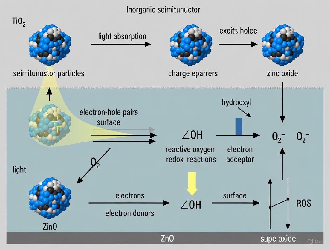
This technical guide provides a comprehensive breakdown of the fundamental mechanisms underlying heterogeneous photocatalysis with inorganic semiconductors. Framed within broader thesis research on reaction principles, this whitepsper systematically details the sequential processes from initial photon absorption to subsequent surface redox reactions. We examine the critical parameters governing each step, present quantitative data on representative photocatalyst systems, outline essential experimental methodologies, and visualize key mechanistic pathways. The information presented herein aims to equip researchers and scientists with a foundational understanding of photocatalytic principles relevant to energy and environmental applications, including solar fuel production and environmental remediation.
Heterogeneous photocatalysis represents a multidisciplinary field centered on utilizing photon energy to drive chemical reactions using semiconductor materials. This process mimics natural photosynthesis by converting solar energy into chemical energy [4]. The foundational discovery, often termed the Honda-Fujishima effect, was demonstrated in 1972 with the photoelectrochemical water splitting using a titanium dioxide (TiO₂) electrode [19] [20]. This discovery sparked extensive research into semiconductor photocatalysts for various applications, including hydrogen production via water splitting, carbon dioxide reduction, and pollutant degradation [4] [19] [5].
A photocatalytic reaction is initiated when a photoexcited electron is promoted from the filled valence band (VB) of a semiconductor photocatalyst to the empty conduction band (CB), provided the absorbed photon energy (hυ) equals or exceeds the semiconductor's band gap energy (Eg) [20]. This results in the formation of an electron-hole pair (e⁻–h⁺) [20]. The subsequent spatial separation and migration of these charge carriers to the semiconductor surface enables them to participate in reduction and oxidation reactions with adsorbed species, respectively [19]. The efficiency of the entire process depends on a delicate balance between the competing processes of charge carrier generation, separation, migration, and recombination [19] [21].
Step-by-Step Mechanistic Breakdown
Step 1: Photon Absorption and Electron-Hole Pair Generation
The photocatalytic process commences with the absorption of light. When a semiconductor photocatalyst is illuminated by light with energy equal to or greater than its bandgap energy, an electron (e⁻) in the valence band absorbs the photon's energy and is excited across the band gap to the conduction band [20]. This transition leaves behind a positively charged vacancy in the valence band, known as a hole (h⁺) [20]. The fundamental equation for this photoexcitation is:
Photoexcitation: Semiconductor (e⁻ in VB) + hυ ≥ E₉ → Semiconductor (e⁻ in CB + h⁺ in VB) Or, more simply: SC + hυ → e⁻CB + h⁺VB [20]
The ability of a photocatalyst to absorb light is primarily determined by its band gap energy, which defines the theoretical limit of its solar energy utilization efficiency [19]. Ultraviolet (UV) light constitutes only a minor fraction (~5%) of the total solar spectrum, making the development of visible-light-responsive photocatalysts a paramount importance for practical applications [19] [20].
Step 2: Charge Carrier Separation and Migration
Following photoexcitation, the spatially separated electron and hole must migrate to the surface of the photocatalyst to participate in chemical reactions. This step is critical as the photogenerated charge carriers are highly susceptible to recombination, a process where the electron falls back into the hole, releasing energy as heat or photons and thus becoming unavailable for catalysis [19] [20]. The following reactions describe charge carrier trapping and recombination:
Charge carrier trapping: e⁻CB → e⁻TR (Trapped electron) h⁺VB → h⁺TR (Trapped hole) [20]
Electron-hole recombination: e⁻TR + h⁺VB (or h⁺TR) → e⁻CB + heat [20]
Enhancing the efficiency of charge separation is crucial for the overall photocatalytic efficiency [19]. Strategies to improve this include coupling with other semiconductors to form heterojunctions, modifying crystal facets, and defect engineering [19] [21]. The lifetime of separated charge carriers is typically in the picosecond to nanosecond range, and their effective separation prolongs their availability for surface reactions [20].
Step 3: Surface Redox Reactions
The final stage involves the trapped electrons and holes reaching the catalyst surface and interacting with adsorbed species. The hole, a powerful oxidant, can directly oxidize an organic donor molecule (D) or react with water or hydroxide ions to generate hydroxyl radicals (•OH), which are non-selective, potent oxidants [20]. Concurrently, the electron, a potent reductant, typically reduces molecular oxygen (O₂) adsorbed on the catalyst surface, forming superoxide radical anions (O₂•⁻) [4] [20]. These reactive oxygen species (ROS) are integral to oxidative degradation processes.
The primary surface reactions in an aqueous medium are outlined below [20]:
Oxidation Pathways:
- Direct oxidation: D + h⁺VB → D•⁺ (Oxidized donor)
- Hydroxyl radical generation: H₂O + h⁺VB → •OH + H⁺ or OH⁻ + h⁺VB → •OH
- Organic radical formation: R-H + •OH → R• + H₂O
Reduction Pathways:
- Oxygen reduction: O₂ + e⁻CB → O₂•⁻
- Protonation of superoxide: O₂•⁻ + H⁺ → HOO•
- Hydrogen peroxide formation: HOO• + e⁻CB → HOO⁻ followed by HOO⁻ + H⁺ → H₂O₂
These reactive intermediates (e.g., •OH, h⁺, O₂•⁻, HOO•) act concomitantly to oxidize a wide variety of organic pollutants [20]. For water splitting, the half-reactions are: the reduction of protons to H₂ by electrons and the oxidation of water to O₂ by holes [19].
Quantitative Data for Representative Photocatalysts
The photocatalytic activity of a material is intrinsically linked to its electronic structure. The band gap energy determines the range of light absorption, while the relative positions of the valence and conduction bands dictate the thermodynamic feasibility of various redox reactions.
Table 1: Band Gap and Characteristics of Common Inorganic Semiconductor Photocatalysts
| Photocatalyst | Band Gap (eV) | Primary Light Absorption Range | Key Applications | Remarks |
|---|---|---|---|---|
| TiO₂ (Rutile/Anatase) | ~3.0 - 3.2 eV [20] | Ultraviolet (UV) | Water splitting [19], pollutant degradation [20] [5] | Widely studied; requires UV activation. |
| ZnO | ~3.2 eV [4] | Ultraviolet (UV) | Organic synthesis [5], water treatment [5] | Similar bandgap to TiO₂. |
| WO₃ | ~2.6 - 2.8 eV [4] | Visible Light | Oxidation reactions [4] | Visible-light-responsive. |
| CdS | ~2.4 eV [4] | Visible Light | Hydrogen evolution [4] | Good visible light absorption but suffers from photocorrosion. |
| g-C₃N₄ | ~2.7 eV [21] | Visible Light (~450 nm) [21] | Water splitting [21], CO₂ reduction [21] | Metal-free, organic semiconductor. |
| NaTaO₃ | ~4.0 eV [19] | Ultraviolet (UV) | Water splitting [19] | High crystallinity and surface nanostructure enhance activity. |
Table 2: Key Reactive Species in Photocatalytic Processes and Their Roles
| Reactive Species | Formation Pathway | Primary Role in Photocatalysis |
|---|---|---|
| Photogenerated Hole (h⁺) | Direct product of photoexcitation [20]. | Powerful oxidant; can directly oxidize pollutants or generate •OH from H₂O/OH⁻ [20]. |
| Hydroxyl Radical (•OH) | H₂O/OH⁻ + h⁺VB → •OH + H⁺ [20]. | Highly potent, non-selective oxidant for degrading organic contaminants [20] [5]. |
| Superoxide Anion (O₂•⁻) | O₂ (ads) + e⁻CB → O₂•⁻ [20]. | A reductant and oxidant; leads to formation of H₂O₂ and other ROS [20]. |
| Hydrogen Peroxide (H₂O₂) | HOO• + e⁻CB → HOO⁻; HOO⁻ + H⁺ → H₂O₂ [20]. | Can be photolyzed to form more •OH radicals [4]. |
Essential Experimental Methodologies
Protocol for Evaluating Photocatalytic Activity for Pollutant Degradation
A standard experimental setup for assessing photocatalytic degradation of pollutants in aqueous solution involves the following steps [20] [5]:
- Reactor Setup: A common configuration is a slurry batch reactor, typically a Pyrex glass vessel, equipped with a magnetic stirrer to keep the photocatalyst particles in suspension. The light source (e.g., Xenon lamp with appropriate filters to simulate solar spectrum or select specific wavelengths) is positioned at a fixed distance from the reactor.
- Reaction Mixture Preparation: A known volume (e.g., 100-200 mL) of the pollutant solution at a specific initial concentration (e.g., 10-50 mg/L) is added to the reactor. A precisely weighed amount of the photocatalyst powder (e.g., 0.5 - 1.0 g/L) is added to the solution.
- Adsorption-Desorption Equilibrium: Before illumination, the suspension is stirred in the dark for a predetermined period (typically 30-60 minutes) to establish an adsorption-desorption equilibrium between the pollutant and the photocatalyst surface. This step is crucial for obtaining an accurate baseline.
- Illigation and Sampling: The light source is turned on, marking time zero (t = 0). At regular time intervals (e.g., every 15-30 minutes), small aliquots (e.g., 3-5 mL) of the suspension are withdrawn from the reactor.
- Sample Analysis: The withdrawn samples are centrifuged or filtered through a membrane (e.g., 0.22 or 0.45 µm) to remove the photocatalyst particles. The clear filtrate is then analyzed to determine the residual concentration of the pollutant. Common analytical techniques include:
- UV-Vis Spectrophotometry: Monitoring the decrease in the characteristic absorption peak of the pollutant.
- High-Performance Liquid Chromatography (HPLC): For more precise quantification and to track the formation of intermediate products.
- Total Organic Carbon (TOC) Analysis: To measure the degree of mineralization (conversion of organic carbon to CO₂).
The degradation efficiency can be calculated as: Efficiency (%) = [(C₀ - Cₜ) / C₀] × 100, where C₀ is the initial concentration after the dark adsorption period and Cₜ is the concentration at time t.
Protocol for Photocatalytic Hydrogen Evolution via Water Splitting
The experimental setup for measuring photocatalytic water splitting activity, particularly for H₂ evolution, requires an airtight system and often the use of a sacrificial agent [19].
- Reactor Setup: A top-irradiation or side-irradiation reaction vessel made of quartz or Pyrex is connected to a closed gas circulation system. The system is thoroughly evacuated to remove air before the reaction.
- Reaction Mixture Preparation: The photocatalyst powder (e.g., 50-100 mg) is dispersed in an aqueous solution (e.g., 100-200 mL). To consume the photogenerated holes and thereby suppress electron-hole recombination, a sacrificial reagent is typically added. Common sacrificial reagents for H₂ evolution include methanol, lactic acid, or triethanolamine (typically 10-20 vol%).
- Co-catalyst Loading: To enhance H₂ evolution kinetics, a co-catalyst (e.g., Pt, Au, Ni) is often photodeposited or impregnated onto the photocatalyst surface. Pt is a common choice due to its low overpotential for proton reduction.
- Reaction and Analysis: The reaction mixture is sealed and evacuated. The light source is turned on to initiate the reaction. The reaction is usually maintained at constant temperature (e.g., 25°C) using a water-cooling jacket. The evolved gases (H₂ and, in overall water splitting, O₂) are periodically analyzed using gas chromatography (GC) equipped with a thermal conductivity detector (TCD) and a molecular sieve column.
The Scientist's Toolkit: Key Research Reagent Solutions
Successful experimentation in photocatalysis relies on a set of essential materials and reagents, each serving a specific function in the synthesis, characterization, and activity testing of photocatalysts.
Table 3: Essential Materials and Reagents for Photocatalysis Research
| Category / Item | Specific Examples | Function / Application |
|---|---|---|
| Core Photocatalysts | TiO₂ (P25 is a common benchmark), ZnO, WO₃, CdS, g-C₃N₄, novel perovskites [4] [19] [20]. | The active material that absorbs light and catalyzes the redox reaction. |
| Precursors for Synthesis | Metal alkoxides (e.g., Ti tetra-isopropoxide for TiO₂), metal salts (nitrates, chlorides), urea or melamine for g-C₃N₄ [20] [21]. | Used in the fabrication of semiconductor photocatalysts via sol-gel, precipitation, or thermal condensation methods. |
| Sacrificial Agents | Methanol, Triethanolamine, Lactic Acid, Ethylenediaminetetraacetic Acid (EDTA) [19]. | Electron donors (for H₂ evolution) or acceptors (for O₂ evolution) that scavenge photogenerated holes or electrons to enhance charge separation. |
| Co-catalysts | Platinum (H₂PtCl₆), Gold, Nickel, Manganese Oxide (MnOx), Cobalt Oxide (CoOx) [19] [21]. | Nanoparticles deposited on the photocatalyst surface to provide active sites and lower the overpotential for H₂ evolution or O₂ evolution reactions. |
| Target Reactants | Methylene Blue, Rhodamine B, Phenol, 4-Chlorophenol, Methylene Blue (for degradation) [20] [5]. H₂O (with sacrificial agents or for overall splitting) [19]. | Model compounds used to quantitatively evaluate the photocatalytic activity and efficiency. |
| Analytical Standards & Reagents | Certified gas standards (H₂ in N₂, O₂ in N₂, CO₂), pure solvents for HPLC (Acetonitrile, Water), TOC calibration standards. | Used for calibration and quantitative analysis of reaction products and remaining reactants via GC, HPLC, and TOC analyzers. |
Reactive Oxygen Species (ROS) are highly reactive chemicals derived from molecular oxygen, playing dual roles as both destructive agents in oxidative stress and constructive signaling molecules in physiological processes [22] [23]. This technical guide provides an in-depth examination of three core ROS—hydroxyl radical, superoxide, and hydrogen peroxide—within the context of inorganic semiconductor photocatalysis reaction principles. We summarize their distinct chemical properties, biological functions, and generation mechanisms, with particular emphasis on photocatalytic ROS production pathways relevant to environmental remediation and therapeutic applications. The document includes standardized experimental protocols for ROS detection, detailed reagent solutions, and visualization of key reaction mechanisms to support research and development efforts in semiconductor photocatalysis and pharmaceutical development.
Reactive Oxygen Species (ROS) encompass a range of molecules with oxidizing properties, including free radicals like superoxide (O₂•⁻) and hydroxyl radicals (•OH), as well as non-radical species such as hydrogen peroxide (H₂O₂) [23] [24]. These compounds are intrinsic to cellular functioning, present at low and stationary levels in normal cells where they participate in essential signaling and homeostasis [23]. The "oxygen paradox" describes the fundamental challenge aerobic organisms face: while oxygen is indispensable for life, it also generates dangerous by-products through its metabolic reduction [22].
In semiconductor photocatalysis, ROS generation represents a crucial mechanism for driving redox reactions aimed at environmental remediation and energy production [4]. When photocatalysts such as TiO₂, ZnO, or CdS absorb photons with energy equal to or greater than their bandgap energy, electrons are excited from the valence band to the conduction band, creating electron-hole pairs [4]. These photogenerated charge carriers can then react with surface-adsorbed H₂O, O₂, and OH⁻ to yield various ROS species, which subsequently participate in oxidative degradation of organic pollutants [4]. Understanding the specific roles, reactivity, and detection methods for each major ROS is thus fundamental to advancing photocatalytic research and applications.
Characterization of Key ROS Species
Chemical Properties and Comparative Analysis
The three primary ROS species exhibit distinct chemical behaviors that dictate their biological and photocatalytic roles. Table 1 summarizes their fundamental properties.
Table 1: Comparative Properties of Key Reactive Oxygen Species
| Property | Hydroxyl Radical (•OH) | Superoxide (O₂•⁻) | Hydrogen Peroxide (H₂O₂) |
|---|---|---|---|
| Chemical Formula | HO• | O₂•⁻ | H₂O₂ |
| Molecular Weight (g·mol⁻¹) | 17.007 [25] | 31.998 [26] | 34.014 [27] |
| Nature | Free Radical | Free Radical | Non-radical Oxidant |
| Reactivity | Extremely high (reacts at diffusion-limited rates) [28] | Moderate (can act as both oxidant and reductant) [29] | Relatively low (requires activation) [23] |
| Half-Life | ~10⁻⁹ seconds [25] [28] | Seconds to minutes (depending on environment) | Relatively stable |
| Membrane Permeability | Limited (highly reactive) | Poor (charged species) [22] | Good (diffuses through aquaporins) [24] |
| Primary Detection Methods | Spin trapping + EPR, fluorescence probes [26] | Cytochrome c reduction, NBT test, chemiluminescence [29] | Fluorometric assays, peroxidase-based methods [27] |
Individual ROS Profiles
Hydroxyl Radical (•OH)
The hydroxyl radical is the most reactive and chemically aggressive ROS, with an oxidation potential of 2.8 eV [28]. It is the neutral form of the hydroxide ion and contains an unpaired electron [25]. Its extreme reactivity leads to a half-life of approximately 10⁻⁹ seconds, during which it can damage virtually all types of macromolecules: carbohydrates, nucleic acids (causing mutations), lipids (initiating lipid peroxidation), and amino acids [25] [28]. Unlike superoxide, hydroxyl radicals cannot be eliminated by specific enzymatic reactions, making them particularly dangerous to biological systems [25] [28]. In photocatalytic systems, •OH represents the primary oxidative species responsible for non-selective degradation of organic pollutants [4].
Superoxide (O₂•⁻)
Superoxide anion represents the first intermediate in the stepwise reduction of molecular oxygen to water [26]. It is formed by the monovalent reduction of oxygen and can act as both an oxidant and a reductant in biological systems [29]. Although less reactive than •OH, superoxide serves as a precursor to more damaging ROS species through secondary reactions [22]. It does not easily cross cellular membranes due to its charge, making its actions more localized [22]. In phagocytic cells, superoxide production via NADPH oxidase constitutes a crucial defense mechanism against pathogens [29]. In photocatalytic contexts, superoxide forms when photogenerated electrons reduce molecular oxygen at the semiconductor surface [4].
Hydrogen Peroxide (H₂O₂)
Hydrogen peroxide is the simplest peroxide, featuring an oxygen-oxygen single bond [27]. It is more stable than radical ROS species but can be activated to form hydroxyl radicals via Fenton or Haber-Weiss reactions in the presence of transition metals [28] [24]. H₂O₂ is membrane-permeable and can diffuse across biological membranes through aquaporin channels [24]. At low concentrations, it functions as an important signaling molecule in physiological processes; at high concentrations, it becomes toxic to cells [23] [24]. In photocatalysis, H₂O₂ forms both through the disproportionation of superoxide and the direct two-electron reduction of oxygen [4].
ROS Generation Pathways in Photocatalysis
Fundamental Photocatalytic Mechanisms
In semiconductor photocatalysis, ROS generation follows a well-defined sequence of events initiated by photon absorption. Figure 1 illustrates the primary reaction pathways in a heterogeneous photocatalytic system.
Figure 1: Primary ROS Generation Pathways in Semiconductor Photocatalysis
The photocatalytic process begins when a semiconductor absorbs a photon with energy (hν) equal to or greater than its bandgap energy (E_g), promoting an electron from the valence band (VB) to the conduction band (CB), thus creating an electron-hole pair (e⁻ CB/h⁺ VB) [4]:
The photogenerated charge carriers then migrate to the catalyst surface where they participate in redox reactions with adsorbed species. The hole (h⁺ VB) possesses strong oxidizing power and can directly oxidize organic compounds or react with water/hydroxyl ions to produce hydroxyl radicals [4]:
Meanwhile, the excited electron (e⁻ CB) can reduce molecular oxygen to superoxide [4]:
Superoxide subsequently undergoes disproportionation to form hydrogen peroxide [4]:
Hydrogen peroxide can then be reduced to hydroxyl radicals through photolytic or catalytic pathways [4]:
Secondary Reaction Pathways
Several secondary reactions contribute to ROS generation and interconversion in photocatalytic systems. The Haber-Weiss reaction and Fenton chemistry play particularly important roles in •OH production:
Haber-Weiss Reaction:
Fenton Reaction:
In semiconductor systems, transition metal impurities or intentionally incorporated dopants can catalyze Fenton-like reactions, enhancing •OH production and overall photocatalytic efficiency [28] [24].
Experimental Protocols for ROS Detection
Hydroxyl Radical Detection
Fluorescence Probe Method
Principle: Hydroxyl radicals react with non-fluorescent compounds to form highly fluorescent products. Common probes include terephthalic acid, which reacts with •OH to form 2-hydroxyterephthalic acid.
Procedure:
- Prepare 0.2 mM terephthalic acid solution in alkaline condition (pH ~10)
- Add the solution to your photocatalytic system
- Illuminate the system with appropriate light source
- Collect aliquots at regular time intervals
- Measure fluorescence intensity at excitation 315 nm / emission 425 nm
- Quantify •OH concentration using a calibration curve with standard 2-hydroxyterephthalic acid solutions
Applications: Suitable for quantifying •OH generation in aqueous photocatalytic systems; can be adapted for time-resolved measurements [28].
Electron Paramagnetic Resonance (EPR) with Spin Trapping
Principle: Short-lived •OH radicals are trapped by spin traps (e.g., DMPO) forming stable adducts detectable by EPR spectroscopy.
Procedure:
- Prepare 100 mM spin trap solution (e.g., DMPO) in appropriate solvent
- Add to photocatalytic system ensuring anaerobic conditions when necessary
- After irradiation, transfer sample to flat cell for EPR measurement
- Record spectrum using typical parameters: modulation frequency 100 kHz, modulation amplitude 1 G, microwave power 20 mW
- Identify DMPO-OH adduct with characteristic 1:2:2:1 quartet signal (aN = aH = 14.9 G)
Applications: Direct detection and identification of free radical species; provides structural information about radical adducts [26].
Superoxide Detection
Nitroblue Tetrazolium (NBT) Reduction Assay
Principle: NBT is reduced by O₂•⁻ to form blue formazan precipitate, providing visible color change.
Procedure:
- Prepare 0.5 mM NBT solution in appropriate buffer (e.g., phosphate buffer pH 7.4)
- Add to photocatalytic system
- Illuminate with appropriate light source
- Monitor absorbance at 560 nm over time
- Calculate superoxide concentration using extinction coefficient ε = 28,000 M⁻¹cm⁻¹
Applications: Simple, cost-effective method for quantifying superoxide production; suitable for initial screening of photocatalytic activity [29].
Cytochrome c Reduction Assay
Principle: Superoxide reduces ferricytochrome c to ferrocytochrome c, producing measurable absorbance change.
Procedure:
- Prepare 50 μM cytochrome c solution in appropriate buffer
- Add to photocatalytic system
- Illuminate with appropriate light source
- Monitor absorbance at 550 nm over time
- Calculate superoxide concentration using Δε550 = 21,000 M⁻¹cm⁻¹
- Include controls with superoxide dismutase to confirm specificity
Applications: Specific detection of superoxide in biological and photocatalytic systems; well-established quantitative method [29].
Hydrogen Peroxide Detection
Fluorometric Assay Using Peroxidase
Principle: Horseradish peroxidase (HRP) catalyzes H₂O₂-mediated oxidation of non-fluorescent substrates to fluorescent products.
Procedure:
- Prepare reaction mixture containing 10 U/mL HRP and 50 μM Amplex Red reagent in appropriate buffer
- Add to samples containing H₂O₂
- Incubate in dark for 30 minutes at room temperature
- Measure fluorescence at excitation 560 nm / emission 590 nm
- Quantify H₂O₂ concentration using standard calibration curve
Applications: Highly sensitive detection of H₂O₂ in complex mixtures; suitable for both biological and photocatalytic systems [27] [24].
The Scientist's Toolkit: Essential Research Reagents
Table 2 compiles key reagents and materials essential for ROS research in photocatalytic and biological contexts.
Table 2: Essential Research Reagents for ROS Studies
| Reagent/Material | Function/Application | Key Characteristics |
|---|---|---|
| Terephthalic Acid | Fluorescent probe for •OH detection | Forms 2-hydroxyterephthalic acid with •OH; excitation/emission at 315/425 nm [28] |
| DMPO (5,5-Dimethyl-1-Pyrroline N-Oxide) | Spin trap for EPR spectroscopy | Forms stable radical adducts with •OH and O₂•⁻; characteristic EPR spectra [26] |
| Nitroblue Tetrazolium (NBT) | Colorimetric superoxide detection | Reduced by O₂•⁻ to purple formazan; absorbance at 560 nm [29] |
| Cytochrome c | Superoxide detection | Reduction measurable at 550 nm; specific for O₂•⁻ [29] |
| Amplex Red | Fluorometric H₂O₂ detection | HRP-coupled assay; excitation/emission at 560/590 nm [27] |
| Superoxide Dismutase (SOD) | Specific O₂•⁻ scavenger | Enzyme that catalyzes O₂•⁻ dismutation to H₂O₂; used in control experiments [29] [26] |
| Catalase | H₂O₂ decomposition enzyme | Specific H₂O₂ scavenger; used to confirm H₂O₂ involvement [24] |
| Mannitol | •OH scavenger | Sugar alcohol that reacts with hydroxyl radicals; scavenging control [25] |
| TiO₂ Nanoparticles | Benchmark photocatalyst | Wide bandgap semiconductor (3.2 eV); UV-activated ROS generation [4] |
Hydroxyl radicals, superoxide, and hydrogen peroxide represent the core reactive oxygen species in both biological systems and semiconductor photocatalysis applications. Their distinct chemical properties, generation pathways, and detection methodologies require specialized experimental approaches. The protocols and reagents detailed in this technical guide provide a foundation for rigorous investigation of ROS in photocatalytic research. Understanding the nuanced roles and behaviors of these species is essential for advancing applications in environmental remediation, energy conversion, and therapeutic development. Future research directions should focus on developing more selective and sensitive detection methods, particularly for real-time monitoring of ROS dynamics in complex systems, and designing photocatalysts with enhanced ROS generation efficiency and specificity.
Inorganic semiconductor photocatalysis has emerged as a cornerstone technology for addressing global challenges in renewable energy and environmental remediation. This whitepaper provides a comprehensive technical analysis of four fundamental material classes—metal oxides, sulfides, phosphides, and carbon-based semiconductors—that are driving innovations in photocatalytic applications. The principles governing these materials, including their electronic structure, charge carrier dynamics, and surface properties, form the critical foundation for developing efficient photocatalytic systems for hydrogen production, CO₂ reduction, and organic pollutant degradation. Framed within broader research on inorganic semiconductor reaction principles, this guide examines the intrinsic and extrinsic parameters that dictate photocatalytic performance, offering researchers and drug development professionals a systematic framework for material selection and optimization in advanced catalytic applications.
Fundamental Principles of Semiconductor Photocatalysis
Photocatalytic Mechanism
Semiconductor photocatalysis operates on the principle of photoexcitation where absorption of photons with energy equal to or greater than the material's bandgap energy (E_g) promotes electrons (e⁻) from the valence band (VB) to the conduction band (CB), simultaneously generating holes (h⁺) in the VB [30] [31]. This process creates electron-hole pairs that migrate to the semiconductor surface to drive reduction and oxidation reactions, respectively. The resulting charge carriers can generate reactive oxygen species (ROS) such as hydroxyl radicals (•OH) and superoxide radicals (•O₂⁻), which possess strong oxidative capabilities for degrading organic pollutants [32] [33].
The overall photocatalytic efficiency depends on three sequential steps: (1) photon absorption and exciton generation, (2) charge carrier separation and migration to surface active sites, and (3) surface redox reactions with adsorbed species [34]. The quantum yield of photocatalytic reactions is often limited by the rapid recombination of photogenerated electron-hole pairs, with time-resolved spectroscopic studies revealing that approximately 90% recombine rapidly after excitation [33].
Band Structure Engineering
The electronic band structure serves as the primary determinant of a semiconductor's photocatalytic capabilities. The bandgap energy dictates the spectral range of light absorption, while the relative positions of the valence and conduction bands govern the thermodynamic feasibility of redox reactions [30].
Table 1: Bandgap Energies and Applications of Semiconductor Classes
| Material Class | Representative Materials | Bandgap Range (eV) | Primary Light Absorption | Key Applications |
|---|---|---|---|---|
| Metal Oxides | TiO₂, ZnO, WO₃, Fe₂O₃ | 2.1-3.6 | UV to Visible | Water treatment, H₂ production [30] [31] |
| Metal Sulfides | CdS, ZnS, CuS, ZnIn₂S₄ | 1.0-2.4 | Visible | H₂ production, CO₂ reduction [34] [35] |
| Metal Phosphides | CoP, Ni₂P, Cu₃P, WP | 1.0-2.0 | Visible | Cocatalysts for H₂ evolution [36] |
| Carbon-Based | g-C₃N₄, Graphene, Carbon dots | 1.6-2.7 | Visible | Pollutant degradation, H₂ production [32] |
For a photocatalytic reaction to proceed efficiently, the conduction band minimum must be more negative than the reduction potential of the target reaction, while the valence band maximum must be more positive than the oxidation potential [30]. Metal oxides typically exhibit wider bandgaps, limiting their activity to UV light, whereas metal sulfides possess narrower bandgaps with broader visible light absorption [34] [30]. The valence bands of most metal sulfides consist of S 3p orbitals, which are more negative than O 2p orbitals found in metal oxides, resulting in narrower bandgaps [34].
Figure 1: Fundamental Photocatalytic Mechanism in Semiconductors
Metal Oxide Semiconductors
Material Properties and Characteristics
Metal oxides represent the most extensively studied class of photocatalytic semiconductors, valued for their exceptional chemical stability, non-toxicity, and robust photocatalytic activity [33] [31]. Titanium dioxide (TiO₂) has emerged as the benchmark photocatalyst due to its high photoreactivity, cost-effectiveness, biological inertness, and photostability [33]. The electronic structure of metal oxides features a configuration where the valence band consists of O 2p orbitals, while the conduction band comprises metal d or sp orbitals [31]. These materials typically exhibit bandgap energies ranging from 2.1 eV (Fe₂O₃) to 3.6 eV (SnO₂), with TiO₂ positioned at approximately 3.2 eV, primarily absorbing in the UV region [30].
The photocatalytic activity of metal oxides originates from two primary sources: the generation of •OH radicals through oxidation of OH⁻ anions and the production of •O₂⁻ radicals via reduction of O₂ [30]. These radical species demonstrate remarkable effectiveness in degrading organic pollutants into less harmful byproducts, ideally mineralizing them to CO₂ and H₂O [33]. The surface morphology of metal oxides critically influences their photocatalytic performance, with nanoscale particles exhibiting enhanced activity due to quantum size effects that increase redox potential and improved charge carrier transport to the surface [30].
Synthesis and Experimental Protocols
Hydrothermal Synthesis of TiO₂ Nanoparticles:
- Precursor Preparation: Mix titanium alkoxide (e.g., titanium isopropoxide) with ethanol under vigorous stirring.
- Hydrolysis: Add the solution dropwise to deionized water maintained at pH 1-3 using nitric acid, resulting in the formation of a white precipitate.
- Aging: Transfer the suspension to a Teflon-lined autoclave and heat at 200°C for 12-24 hours to promote crystallization.
- Washing and Drying: Centrifuge the resulting nanoparticles, wash repeatedly with ethanol and deionized water, and dry at 80°C for 12 hours.
- Calcination: Anneal the powder at 400-500°C for 2-4 hours to obtain the desired crystalline phase (typically anatase) [33] [31].
Sol-Gel Synthesis of ZnO Nanoparticles:
- Solution Preparation: Dissolve zinc acetate dihydrate in ethanol with continuous stirring at 60°C.
- Precipitation: Add a solution of sodium hydroxide in ethanol dropwise to initiate precipitation.
- Aging: Maintain the reaction mixture at 60°C for 2 hours with constant stirring to promote nanoparticle growth.
- Purification: Recover nanoparticles by centrifugation, wash with ethanol, and dry at 80°C.
- Thermal Treatment: Calcinate the powder at 300-400°C to enhance crystallinity [31].
Performance optimization for metal oxides typically involves morphological control to increase surface area, elemental doping to extend light absorption into the visible range, and heterojunction construction with other semiconductors to improve charge separation [30] [31].
Metal Sulfide Semiconductors
Material Properties and Characteristics
Metal sulfides have gained significant attention as visible-light-driven photocatalysts due to their narrow band gaps, exceptional light-harvesting capabilities, and abundant exposed active sites [34]. Representative materials include CdS (Eg ≈ 2.4 eV), ZnS, and complex quaternary sulfides such as Cu₂ZnSnS₄. The electronic structure of metal sulfides features a valence band composed of S 3p orbitals, which are much more negative than O 2p orbitals in metal oxides, resulting in narrower band gaps and broader visible light absorption [34]. The conduction band contains d and sp metal orbitals, contributing to excellent electron mobility and reduction capability [34].
Despite their advantageous optical properties, metal sulfides suffer from limited photoelectrochemical stability due to light-induced photocorrosion, where photogenerated holes oxidize surface sulfide ions (S²⁻) to elemental sulfur (S⁰) or sulfate (SO₄²⁻) [34] [35]. This phenomenon severely hampers their practical implementation and has motivated extensive research into stabilization strategies. Survey data indicates a 4.1-fold increase in publications and a remarkable 171.6-fold increase in citations on metal sulfide photocatalysis from 2011 to 2020, underscoring the growing research interest in this material class [34].
Synthesis and Experimental Protocols
CdS Nanoparticle Synthesis via Hydrothermal Method:
- Precursor Mixing: Dissolve Cd(NO₃)₂ and Na₂S in deionized water separately.
- Reaction: Slowly add the Na₂S solution to the Cd(NO₃)₂ solution with constant stirring, resulting in a yellow precipitate.
- Hydrothermal Treatment: Transfer the suspension to a Teflon-lined autoclave and maintain at 160-200°C for 12-24 hours.
- Product Recovery: Collect the resulting CdS nanoparticles by centrifugation, wash with ethanol and deionized water, and dry at 60°C under vacuum [34] [35].
Photodeposition of Cocatalysts on CdS:
- Suspension Preparation: Disperse CdS nanoparticles in an aqueous solution containing methanol (10-20 vol%) as a sacrificial electron donor.
- Cocatalyst Precursor Addition: Introduce H₂PtCl₆ solution (0.4 wt% Pt relative to CdS) to the suspension.
- Irradiation: Expose the system to visible light (λ ≥ 420 nm) for 1-2 hours with continuous stirring to facilitate Pt nanoparticle deposition.
- CrOx Shell Formation: Add K₂CrO₄ solution to the Pt/CdS suspension and continue irradiation to form a core-shell Pt@CrOx structure [35].
Anti-Photocorrosion Strategy - Oxide Coating: TiO₂ coating on CdS surfaces effectively suppresses photocorrosion by providing a physical barrier against sulfur oxidation while facilitating hole transfer for water oxidation. This is achieved through controlled hydrolysis of titanium precursors followed by calcination at moderate temperatures (300-400°C) [35].
Metal Phosphide Semiconductors
Material Properties and Characteristics
Transition metal phosphides (TMPs) have emerged as highly efficient cocatalysts for enhancing photocatalytic hydrogen evolution, offering advantages including low cost, abundant availability, high electrical conductivity, and favorable physical and chemical properties [36]. Common TMPs include CoP, Ni₂P, Cu₃P, WP, and MoP, which can be synthesized in various morphologies such as nanoparticles, nanosheets, nanorods, and hollow structures [36]. According to their chemical bond types, TMPs can be classified as ionic compounds, metal bond compounds, or covalent bond compounds, with stoichiometries ranging from M₃P to MP₃ [36].
The primary application of TMPs in photocatalysis involves serving as cocatalysts that enhance the apparent quantum efficiency (AQE) of hydrogen evolution reactions [36]. Their functions encompass multiple aspects: (1) improving light absorption capacity through plasmonic effects or sensitization; (2) providing abundant active sites for proton reduction; (3) facilitating charge transfer and separation through efficient electron extraction; (4) optimizing water activation by lowering the energy barrier for water dissociation; and (5) enhancing photostability by protecting the main photocatalyst from degradation [36]. Bimetallic phosphides such as cobalt-nickel phosphides have demonstrated superior performance due to their enhanced metallicity and dual active sites for HER [36].
Synthesis and Experimental Protocols
Solvothermal Synthesis of CoP Nanoparticles:
- Precursor Preparation: Dissolve cobalt acetate and polyvinylpyrrolidone (PVP) in a mixed solvent of oleylamine and octadecene.
- Phosphorization: Add tri-n-octylphosphine (TOP) as the phosphorus source to the solution under inert atmosphere.
- Reaction: Heat the mixture to 300-320°C and maintain for 2-4 hours to facilitate nanoparticle growth.
- Purification: Precipitate the CoP nanoparticles by adding ethanol, collect by centrifugation, and wash repeatedly with cyclohexane and ethanol [36].
Alternative Phosphidation Method Using NaH₂PO₂:
- Support Preparation: Disperse the primary semiconductor (e.g., CdS or g-C₃N₄) in ethanol.
- Impregnation: Add cobalt nitrate solution to the suspension and evaporate the solvent to achieve uniform metal precursor distribution.
- Phosphidation: Place the material together with NaH₂PO₂ in a tube furnace, with NaH₂PO₂ positioned upstream.
- Thermal Treatment: Heat at 300-400°C for 2 hours under N₂ flow to convert the metal precursor to phosphide [36].
Photocatalytic Hydrogen Evolution Testing with TMP Cocatalysts:
- Reactor Setup: Combine TMP-modified photocatalyst (50 mg) with an aqueous solution (100 mL) containing sacrificial agents (e.g., 10 vol% triethanolamine or 0.1 M Na₂S/0.02 M Na₂SO₃).
- Deaeration: Purge the system with N₂ for 30 minutes to remove dissolved oxygen.
- Irradiation: Expose to simulated solar light (300 W Xe lamp with appropriate cutoff filters) with continuous stirring.
- Gas Analysis: Quantify evolved H₂ using gas chromatography with a thermal conductivity detector at regular intervals [36].
Carbon-Based Semiconductors
Material Properties and Characteristics
Carbon-based semiconductors encompass a diverse family of materials including graphene, carbon nanotubes, carbon dots, carbon fibers, graphyne, carbon aerogels, and fullerene [32]. These materials rarely function as standalone photocatalysts but instead serve as exceptional cocatalysts that enhance the performance of primary semiconductors through multiple mechanisms: (1) acting as multifunctional supports to enhance conductivity, adsorption, and catalytic performance; (2) serving as electron mediators to effectively separate electron-hole pairs; (3) functioning as photosensitizers to broaden the light absorption range; (4) providing stabilization to prevent aggregation and corrosion of semiconductors; and (5) forming semiconductor-carbon heterojunctions to facilitate charge separation [32].
Graphene possesses an extensive theoretical specific surface area of 2600 m²/g and a wide π-π conjugate structure that enhances pollutant adsorption and catalytic activity [32]. Carbon dots exhibit unique up-conversion photoluminescence properties, extending light absorption to near-infrared regions [32]. Graphyne, as an emerging carbon allotrope, demonstrates favorable electron-hole pair mobility and adjustable bandgap, showing significant potential in photoelectrocatalysis applications [32].
Synthesis and Experimental Protocols
Preparation of Graphene-Semiconductor Composites:
- Graphene Oxide Synthesis: Employ modified Hummers' method to oxidize graphite to graphene oxide (GO).
- Composite Formation: Dispense GO in water through ultrasonication, add semiconductor precursors (e.g., TiCl₄ for TiO₂), and adjust pH to facilitate deposition.
- Reduction: Hydrothermally treat the mixture at 120-180°C for 12-24 hours to simultaneously reduce GO to reduced graphene oxide (rGO) and crystallize the semiconductor.
- Product Recovery: Collect the composite by filtration or centrifugation, wash thoroughly, and dry at 60°C [32].
Carbon Dot Synthesis via Hydrothermal Carbonization:
- Precursor Preparation: Dissolve carbon-rich precursors (e.g., citric acid) in deionized water.
- Hydrothermal Treatment: Transfer the solution to a Teflon-lined autoclave and heat at 180-250°C for 4-12 hours.
- Purification: Dialyze the resulting solution against deionized water using a membrane (MWCO 1000 Da) to remove unreacted precursors.
- Composite Formation: Combine carbon dots with semiconductor precursors during material synthesis or through post-synthesis mixing [32].
Photoelectrocatalytic Degradation Experiments:
- Electrode Preparation: Deposit carbon-based semiconductor composites on conductive substrates (e.g., FTO glass) using drop-casting, spin-coating, or electrophoretic deposition.
- Reactor Setup: Configure a three-electrode system with the composite as photoanode, Pt wire as counter electrode, and Ag/AgCl as reference electrode in electrolyte containing target pollutants.
- Bias Application: Apply external bias (typically 0.5-1.0 V vs. Ag/AgCl) using a potentiostat while irradiating with simulated solar light.
- Analysis: Monitor pollutant concentration decay using UV-vis spectroscopy or HPLC, and quantify mineralization through TOC measurements [32].
Comparative Analysis and Performance Metrics
Table 2: Comparative Performance of Semiconductor Classes in Photocatalytic Applications
| Material Class | H₂ Evolution Rate (μmol·h⁻¹·g⁻¹) | AQE (%) | Stability | Key Challenges |
|---|---|---|---|---|
| Metal Oxides | TiO₂: 10-100 (UV) | 1-10 (UV) | Excellent | Limited visible light absorption, recombination [33] |
| Metal Sulfides | CdS: 219-568 (visible) | 10.2@450nm | Moderate-Poor | Photocorrosion, toxicity concerns [34] [35] |
| Metal Phosphides | CoP/g-C₃N₄: Enhanced 5-10x | 15-20 | Good | Primarily cocatalysts, synthesis complexity [36] |
| Carbon-Based Composites | rGO/TiO₂: 2-5x improvement | 5-15 | Good-Excellent | Cost, complex fabrication [32] |
The performance metrics in Table 2 illustrate the trade-offs between activity, stability, and practical implementation across material classes. Metal sulfides demonstrate superior visible-light activity but suffer from stability issues, while metal oxides offer stability but limited visible light response. Metal phosphides excel as cocatalysts but rarely function as standalone photocatalysts. Carbon-based materials provide exceptional enhancement capabilities but involve more complex composite fabrication.
Figure 2: Advanced Z-Scheme Configuration for Efficient Water Splitting
Figure 2 illustrates a sophisticated Z-scheme system integrating n-type CdS and BiVO₄ with a [Fe(CN)₆]³⁻/[Fe(CN)₆]⁴⁻ mediator, achieving 10.2% apparent quantum yield at 450 nm with stoichiometric H₂/O₂ evolution [35]. This configuration demonstrates how material classes can be strategically combined to overcome individual limitations, with oxide coatings enhancing stability while maintaining high activity.
The Scientist's Toolkit: Essential Research Reagents and Materials
Table 3: Key Research Reagent Solutions for Photocatalysis Research
| Reagent/Material | Function | Application Context | Considerations |
|---|---|---|---|
| Titanium Isopropoxide (TTIP) | TiO₂ precursor | Metal oxide synthesis | Hydrolysis sensitivity, requires anhydrous handling |
| Cadmium Nitrate Tetrahydrate | Cd²⁺ source for sulfide synthesis | Metal sulfide preparation | Toxicity, requires controlled disposal |
| Sodium Sulfide Nonahydrate | S²⁻ source for sulfide synthesis | Metal sulfide preparation | Moisture sensitivity, releases H₂S |
| Tri-n-octylphosphine (TOP) | Phosphorus source for phosphides | TMP synthesis | Air-sensitive, pyrophoric properties |
| NaH₂PO₂ | Alternative solid P source | Phosphidation processes | Requires inert atmosphere during thermal treatment |
| H₂PtCl₆•6H₂O | Pt precursor for cocatalysts | Noble metal deposition | Concentration controls nanoparticle size |
| K₂CrO₄ | CrOx shell precursor | Core-shell cocatalyst formation | Controls shell thickness and coverage |
| Graphene Oxide (GO) | Carbon support/mediator | Composite fabrication | Degree of oxidation affects electronic properties |
| Ammonium Metavanadate | Vanadium source for BiVO₄ | OEP synthesis | Controls crystal morphology and facet exposure |
| [Fe(CN)₆]³⁻/⁴⁻ salts | Redox mediator | Z-scheme configurations | Concentration ratio critical for charge balance |
The strategic selection and development of semiconductor materials from the four fundamental classes—metal oxides, sulfides, phosphides, and carbon-based semiconductors—provides a versatile toolkit for advancing photocatalytic technologies. Current research trajectories indicate growing emphasis on sophisticated heterostructure design that combines multiple material classes to leverage their complementary advantages while mitigating individual limitations. The integration of computational screening with advanced synthesis techniques is accelerating the discovery of novel compositions with optimized band structures and surface properties. As characterization methods continue to improve, particularly in situ and operando techniques, researchers are developing deeper insights into the interfacial charge transfer processes and reaction mechanisms that govern photocatalytic efficiency. These fundamental advances in understanding inorganic semiconductor reaction principles are paving the way for next-generation photocatalytic systems with enhanced quantum efficiencies and operational stabilities, ultimately supporting broader implementation in energy conversion and environmental protection applications.
From Lab to Life: Material Synthesis, Hybrid Systems, and Real-World Deployments
The fabrication of nanomaterials is a cornerstone of modern scientific research, with profound implications for the advancement of inorganic semiconductor photocatalysis. The selection of synthesis technique directly influences critical photocatalytic properties, including band gap energy, surface-to-volume ratio, charge carrier dynamics, and surface reactivity [37] [38]. While conventional chemical methods have historically enabled precise control over nanomaterial characteristics, they often involve harsh reducing agents, toxic solvents, and energy-intensive processes that raise significant environmental and biocompatibility concerns [37] [39]. In response, green synthesis has emerged as a sustainable alternative that leverages biological entities such as plant extracts, microorganisms, and biomolecules as reducing and stabilizing agents [40] [41]. This technical guide provides a comprehensive comparison of these divergent synthesis paradigms, with specific emphasis on their application in developing advanced photocatalysts for energy conversion and environmental remediation.
Fundamental Principles and Comparative Analysis
Chemical Synthesis Methods
Chemical approaches to nanomaterial fabrication typically employ bottom-up strategies that involve the reduction of metal precursors in solution phases. These methods utilize a range of chemical agents to precisely control nucleation and growth processes [37] [38].
- Reducing Agents: Chemical synthesis frequently employs sodium borohydride (NaBH₄), citrate salts, or hydrazine as potent reducing agents to convert metal ions to their zero-valent states [37].
- Stabilizers and Capping Agents: To prevent aggregation and control particle growth, chemical methods utilize surfactants (e.g., CTAB), polymers (e.g., PVP), or organic ligands that adsorb to nanoparticle surfaces [37] [39].
- Reaction Conditions: Chemical synthesis often requires inert atmospheres, elevated temperatures, and precise pH control to achieve monodisperse nanoparticles with tailored properties [37].
Despite their effectiveness, these methods generate hazardous byproducts and involve toxic chemicals that pose environmental and safety challenges [37] [40]. The complexity of chemical synthesis often necessitates multiple purification steps and raises concerns about residual contaminants on nanoparticle surfaces, which can adversely affect photocatalytic performance [37].
Green Synthesis Principles
Green synthesis represents a paradigm shift toward sustainable nanomaterial fabrication by harnessing nature's inherent chemical capabilities. This approach utilizes biological resources as nano-factories, replacing toxic chemicals with phytochemicals, microbial enzymes, and biomolecules [41] [39].
- Plant-Mediated Synthesis: Plant extracts contain diverse secondary metabolites including phenolic compounds, terpenoids, flavonoids, and alkaloids that function as both reducing and capping agents [39] [42]. The abundance of these natural compounds in various plant parts (leaves, roots, fruits, seeds) enables rapid reduction of metal ions under ambient conditions [39] [38].
- Microbial Synthesis: Microorganisms including bacteria, fungi, and algae can synthesize nanoparticles through enzymatic reduction or biosorption processes [41] [42]. Microbial synthesis often provides enhanced control over crystal morphology but typically proceeds at slower rates compared to plant-mediated approaches [39].
- Biomolecule-Assisted Synthesis: Isolated proteins, peptides, DNA, and carbohydrates can serve as templates for nanoparticle formation, enabling precise control over size and morphology through molecular recognition [42].
The fundamental advantage of green synthesis lies in its inherent sustainability—it consumes less energy, utilizes renewable resources, and generates biodegradable waste [40] [41]. Additionally, the biological capping agents often enhance nanoparticle biocompatibility and functionality for specific applications [39] [42].
Table 1: Comparative Analysis of Synthesis Methods for Photocatalytic Nanomaterials
| Parameter | Chemical Synthesis | Green Synthesis |
|---|---|---|
| Reducing Agents | Sodium borohydride, Citrate, Hydrazine [37] | Plant phenolics, Terpenoids, Microbial enzymes [39] [42] |
| Stabilizing Agents | Synthetic polymers (PVP), Surfactants (CTAB) [37] | Proteins, Polysaccharides, Plant metabolites [39] [42] |
| Reaction Conditions | High temperature, Inert atmosphere, Precise pH [37] | Ambient temperature, Aqueous phase, Broad pH range [39] |
| Energy Consumption | High (heating, stirring, purification) [37] | Low (room temperature processes) [40] [41] |
| Environmental Impact | Toxic byproducts, Hazardous waste [37] [40] | Biodegradable waste, Renewable resources [40] [41] |
| Scalability | Well-established for industrial scale [37] | Emerging for large-scale production [42] |
| Typical Yield | High with optimization [37] | Variable depending on biological source [39] |
| Photocatalytic Relevance | Potential surfactant contamination [37] | Enhanced biocompatibility and surface functionality [38] |
Experimental Protocols
Chemical Synthesis of TiO₂ Nanoparticles (Sol-Gel Method)
The sol-gel method represents a widely employed chemical approach for producing high-purity metal oxide nanoparticles with controlled crystallinity and size distribution [38].
Materials: Titanium alkoxide precursor (e.g., titanium isopropoxide), ethanol, nitric acid, deionized water.
Procedure:
- Solution Preparation: Dilute titanium isopropoxide (0.1 M) in anhydrous ethanol under vigorous stirring.
- Hydrolysis: Slowly add an acidified water solution (pH 1-3 using HNO₃) to the precursor solution in a 1:4 molar ratio (water:precursor) while maintaining continuous stirring.
- Gel Formation: Allow the mixture to react until a transparent sol forms, then age for 24 hours to facilitate gelation.
- Drying and Calcination: Dry the gel at 80°C for 12 hours, then calcine at 400-600°C for 2-4 hours to crystallize the TiO₂ nanoparticles.
- Characterization: Analyze crystal structure using XRD, surface morphology by SEM/TEM, and band gap through UV-Vis spectroscopy [38].
Photocatalytic Considerations: The calcination temperature critically controls the crystalline phase (anatase, rutile, or mixed) which directly influences photocatalytic efficiency. Anatase phase typically exhibits superior activity due to its higher charge carrier mobility and appropriate band edge positions [38].
Plant-Mediated Green Synthesis of ZnO Nanoparticles
ZnO nanoparticles synthesized through green approaches have demonstrated exceptional photocatalytic performance under visible light irradiation [38].
Materials: Zinc acetate dihydrate, plant extract (e.g., Azadirachta indica leaves), deionized water.
Plant Extract Preparation:
- Wash fresh plant leaves thoroughly with deionized water.
- Prepare a 10% (w/v) aqueous extract by boiling chopped leaves in deionized water for 10-15 minutes.
- Filter the extract through Whatman No. 1 filter paper to remove particulate matter [38].
Nanoparticle Synthesis:
- Precursor Solution: Prepare a 0.1 M zinc acetate solution in deionized water.
- Reduction Reaction: Slowly add plant extract to the precursor solution in a 1:4 ratio under continuous stirring.
- pH Adjustment: Maintain the solution pH between 9-11 using sodium hydroxide to optimize reduction efficiency.
- Incubation and Recovery: Incubate the mixture at 60-80°C for 1-2 hours until a precipitate forms. Centrifuge the resulting suspension at 10,000 rpm for 15 minutes.
- Purification and Annealing: Wash the pellet multiple times with deionized water and ethanol, then dry at 80°C and anneal at 400°C for 2 hours to obtain crystalline ZnO nanoparticles [38].
Mechanistic Insight: The polyphenols and terpenoids present in the plant extract facilitate zinc ion reduction, while proteins and carbohydrates act as capping agents that control particle growth and prevent aggregation [39] [42]. The green-synthesized ZnO nanoparticles often exhibit reduced band gaps and enhanced visible-light absorption compared to chemically synthesized counterparts, attributed to surface functionalization with organic moieties [38].
Advanced Characterization Techniques
Comprehensive characterization is essential to correlate synthesis parameters with photocatalytic performance:
- Structural Analysis: XRD determines crystal structure, phase purity, and crystallite size through Scherrer analysis [39] [38].
- Morphological Assessment: SEM and TEM reveal particle size distribution, shape, and aggregation state [39] [42].
- Optical Properties: UV-Vis spectroscopy calculates band gap energy using Tauc plots, while photoluminescence spectroscopy assesses charge carrier recombination rates [21] [38].
- Surface Characterization: FTIR identifies functional groups from capping agents, while BET analysis measures specific surface area and porosity [39] [38].
- Elemental Composition: EDS and XPS determine chemical composition and oxidation states of constituent elements [42].
Table 2: Key Reagent Solutions for Nanomaterial Synthesis
| Reagent Category | Specific Examples | Function in Synthesis | Photocatalytic Relevance |
|---|---|---|---|
| Chemical Precursors | Titanium isopropoxide, Zinc acetate, Chloroauric acid [37] [38] | Source of metal ions for nanoparticle formation | Determines composition, crystal structure, and intrinsic band gap [38] |
| Chemical Reducing Agents | Sodium borohydride, Trisodium citrate, Hydrazine hydrate [37] | Convert metal ions to zero-valent or oxide states | Potential surface contamination affects active sites [37] |
| Green Reducing Agents | Plant extracts (Azadirachta indica, Aloe vera), Microbial cultures [39] [38] | Phytochemicals and enzymes reduce metal ions | Surface functionalization can enhance visible light absorption [38] |
| Stabilizing Agents | PVP, CTAB, Plant proteins, Polysaccharides [37] [39] | Control particle growth and prevent aggregation | Affects surface area and accessibility of active sites [37] [39] |
| Solvents | Deionized water, Ethanol, Methanol [37] [38] | Reaction medium for nanoparticle formation | Water as solvent improves environmental compatibility [38] |
Synthesis Workflows and Mechanistic Pathways
The following diagrams illustrate the fundamental workflows and mechanistic relationships in chemical versus green synthesis approaches for photocatalytic nanomaterials.
Synthesis Workflow: Chemical Method
Synthesis Workflow: Green Method
Impact on Photocatalytic Performance
The synthesis method profoundly influences the photocatalytic efficiency of nanomaterials through multiple mechanistic pathways:
Charge Carrier Dynamics
In photocatalytic processes, semiconductor nanomaterials absorb photons with energy exceeding their band gap, generating electron-hole pairs that drive redox reactions [21] [38]. Green-synthesized nanoparticles often exhibit modified surface states due to biomolecular capping, which can create intermediate energy levels that reduce charge carrier recombination [38]. Chemically synthesized materials typically have cleaner surfaces but may require cocatalyst deposition (e.g., Pt, Au) to achieve efficient charge separation [21].
Band Gap Engineering
The band gap energy determines the spectral response of photocatalysts. Green synthesis approaches frequently yield nanoparticles with narrowed band gaps compared to their chemically synthesized counterparts, extending light absorption into the visible spectrum [38]. This phenomenon is attributed to surface complexation between metal atoms and organic functional groups from biological extracts, which creates additional electronic states within the band structure [42] [38].
Surface Reactivity and Active Sites
The surface characteristics of photocatalysts dictate their interaction with reactant molecules. Green-synthesized nanomaterials possess biologically derived surface functionalities that can enhance adsorption capacity for organic pollutants through various intermolecular interactions [38]. However, excessive surface coverage by capping agents may potentially block active sites, requiring optimization of biomass-to-precursor ratios during synthesis [39].
Table 3: Photocatalytic Performance of Select Nanomaterials by Synthesis Method
| Photocatalyst | Synthesis Method | Key Structural Features | Photocatalytic Performance | Application Reference |
|---|---|---|---|---|
| TiO₂ Nanoparticles | Chemical (Sol-Gel) [38] | Controlled anatase phase, High crystallinity | Efficient UV-driven dye degradation | Environmental remediation [38] |
| ZnO Nanoparticles | Plant-mediated green synthesis [38] | Reduced band gap (2.8-3.0 eV), Biomolecular capping | Enhanced visible-light activity | Dye degradation, ~95% efficiency [38] |
| CeO₂ Nanoparticles | Green synthesis using Rheum turkestanicum [37] | Cubic fluorite structure, 30 nm spherical particles | Photocatalytic dye degradation | Wastewater treatment [37] |
| Ag-doped ZnO/CaO | Green synthesis with Caccinia macranthera [37] | 23 nm spherical particles, Doped structure | Antibacterial and photocatalytic activity | Environmental and biomedical [37] |
The selection between green and chemical synthesis methods for photocatalytic nanomaterials involves balancing multiple considerations, including sustainability, economic viability, precise control, and final application requirements. Chemical methods offer superior control over crystallinity, phase composition, and morphology, which are critical parameters for photocatalytic efficiency [37] [38]. Conversely, green synthesis provides compelling advantages through reduced environmental impact, lower energy consumption, and inherent biocompatibility [40] [41].
Future research should focus on hybrid approaches that combine the precision of chemical synthesis with the sustainability of green principles. Microwave-assisted synthesis represents one such promising direction, offering rapid heating, uniform nucleation, and reduced energy consumption while compatible with green precursors [43]. Additionally, advancing our understanding of structure-activity relationships in green-synthesized photocatalysts will enable more targeted design of these materials [42] [38]. As the field progresses, standardization of green synthesis protocols and comprehensive life-cycle assessments will be essential for translating laboratory innovations into commercially viable photocatalytic technologies that address pressing environmental and energy challenges [41] [42].
The pursuit of efficient solar energy conversion and environmental remediation has positioned inorganic semiconductor photocatalysis as a cornerstone of modern materials science research. The performance of these photocatalytic systems is fundamentally governed by their ability to absorb light and separate photogenerated charge carriers effectively. Advanced material architectures, including heterostructures, doped semiconductors, and two-dimensional (2D) materials, provide sophisticated strategies to manipulate these critical processes at the nanoscale. This technical guide examines the design principles, synthesis methodologies, and structure-property relationships of these advanced architectures within the context of inorganic semiconductor photocatalysis reaction mechanisms. By integrating foundational theory with recent experimental breakthroughs, this work aims to equip researchers with the knowledge to design next-generation photocatalytic materials with enhanced quantum efficiencies and practical applicability.
Fundamental Charge Transfer Principles in Photocatalysis
The photocatalytic process initiates with the generation of electron-hole pairs upon light absorption when photon energy (hν) meets or exceeds the semiconductor's bandgap energy (Eg). For a semiconductor like TiO₂, this process can be represented as: TiO₂ + hν → TiO₂ (ecb⁻ + hvb⁺) where ecb⁻ represents a conduction band electron and hvb⁺ represents a valence band hole [44].
The ensuing dynamics critically determine photocatalytic efficiency. Charge carrier recombination, which occurs on timescales from femtoseconds to nanoseconds, competes directly with the charge carrier transfer to adsorbed species, which typically occurs on nanosecond to microsecond timescales [44]. The relatively longer transfer time compared to recombination means most photogenerated carriers are lost without participating in redox reactions. Advanced material architectures aim to tip this balance by introducing internal electric fields, creating trapping sites, or providing spatial pathways that physically separate electrons and holes, thereby reducing recombination probability.
Table 1: Key Kinetic Parameters in Photocatalytic Charge Transfer
| Process | Typical Timescale | Determining Factors | Influence on Efficiency |
|---|---|---|---|
| Charge Generation | Femtoseconds (fs) | Light intensity, absorption coefficient | Determines initial carrier density |
| Bulk Recombination | Picoseconds (ps) to nanoseconds (ns) | Defect density, crystal quality | Major efficiency loss; should be minimized |
| Surface Trapping | Picoseconds (ps) | Surface area, defect states | Can inhibit recombination if controlled |
| Charge Transfer to Adsorbates | Nanoseconds (ns) to microseconds (µs) | Surface chemistry, energy level alignment | Desired pathway for catalytic reactions |
Heterostructure Architectures for Charge Separation
Heterostructures, comprising interfaces between two or more semiconductors, represent a powerful design strategy for achieving spatial separation of photogenerated electrons and holes.
Design and Classification
The electronic structure at the heterojunction interface dictates charge flow. In a type-II staggered band alignment, the conduction band minimum (CBM) and valence band maximum (VBM) of one semiconductor are both higher than those of the other. This alignment drives electrons to the semiconductor with the lower CBM and holes to the one with the higher VBM, achieving natural charge separation [45]. More recently, S-scheme (Step-scheme) heterojunctions have been developed, which selectively recombine less useful carriers at the interface through an internal electric field, leaving the most redox-potent electrons and holes to participate in reactions [46].
Exemplary Heterostructure Systems
- Bi₂SiO₅/β-Bi₂O₃ Systems: This system combines n-type Bi₂SiO₅ with p-type β-Bi₂O₃, forming a p-n heterojunction. The internal electric field at the interface drastically improves charge separation. Quantum-chemical calculations of the 2D layered interface predict modified optical properties and enhanced photocatalytic activity [45].
- Bi₂Sn₂O₇-Based Heterostructures: Pyrochlore-type Bi₂Sn₂O₇ exhibits strong visible-light absorption and high stability. Constructing Z-scheme and S-scheme heterostructures with this material effectively reduces charge recombination, boosting performance for pollutant degradation [46].
- CdS/MoS₂ Heterojunction: Derived from a Cd-metal organic framework (MOF) precursor, this heterojunction improves charge separation efficiency and visible-light photocatalytic activity [47].
Figure 1: Charge Transfer in a Type-II Heterojunction. Electrons (e⁻) and holes (h⁺) are spatially separated at the interface, directing them to different semiconductors where they participate in reduction and oxidation reactions, respectively.
Doping Strategies for Bandgap Engineering
Doping introduces foreign atoms into a host semiconductor lattice to deliberately modify its electronic structure, enhancing light absorption and charge carrier dynamics.
Doping Mechanisms and Effects
Doping operates through two primary mechanisms: substitutional doping, where foreign atoms replace host atoms in the lattice, and intercalation doping, where guest atoms/molecules are inserted between layers [48]. These processes create new energy levels within the bandgap, reduce the effective bandgap energy, introduce charge carriers (electrons or holes), and create surface defects or oxygen vacancies that can act as active sites [49].
Advanced Doping Techniques
- Plasma Doping: This rapid, energy-efficient technique uses ionized gas (plasma) containing reactive species (electrons, ions, radicals) to introduce dopants. It enhances surface area, introduces functional groups, creates oxygen vacancies, and reduces bandgap energy without altering the bulk structure. Common plasma sources include nitrogen, hydrogen, air, oxygen, and argon [49].
- Photocatalytic Doping of Organic Semiconductors: A groundbreaking method uses photocatalysts (e.g., acridinium derivatives) with air as a weak oxidant to dope organic semiconductors at room temperature. The photocatalyst acts as an electron shuttle, enabling efficient doping with conductivities exceeding 3,000 S cm⁻¹ [50].
Table 2: Comparison of Semiconductor Doping Techniques
| Doping Method | Key Mechanism | Advantages | Limitations |
|---|---|---|---|
| Sol-Gel | Chemical reaction in solution | Good stoichiometry control, low temperature | Long processing time, possible agglomeration |
| Chemical Vapor Deposition (CVD) | Vapor-phase reaction | High purity, uniform films | High temperature, complex equipment |
| Hydrothermal | Reaction in aqueous solution | Good crystallinity, simple setup | Pressure control required, batch process |
| Plasma Doping [49] | Gaseous plasma-surface interaction | Rapid, low-temperature, high doping efficiency | Uniformity on complex geometries, reactor design |
Two-Dimensional (2D) Materials and Heterostructures
2D materials, characterized by their atomically thin layers and strong in-plane bonds, offer exceptional physicochemical properties tailor-made for photocatalysis.
Properties and Advantages
The ultra-high surface-to-volume ratio of 2D materials provides abundant surface active sites for catalytic reactions. Their unique electronic structure often leads to a layer-dependent bandgap, allowing optical and electronic properties to be tuned by varying the number of layers. Furthermore, the shortened charge migration distance from the material's bulk to its surface significantly reduces recombination losses [51] [52].
Key 2D Material Families
- Transition Metal Dichalcogenides (TMDs): Materials like MoS₂ and WS₂, with formula MX₂ (M=transition metal, X=chalcogen), are direct-bandgap semiconductors in the monolayer form. Their photocatalytic active sites differ from electrocatalytic ones, with oxidation products localizing at excitation spots (stationary holes) while reduction occurs microns away due to high electron mobility [53].
- Graphene and Derivatives: Graphene oxide (GO) and reduced GO (rGO) are often used as conductive supports in composite photocatalysts, facilitating electron extraction and transport, thereby suppressing charge recombination [51].
- MXenes: Two-dimensional carbides, nitrides, and carbonitrides offer high electrical conductivity and tunable surface chemistry, making them excellent co-catalysts [52].
- g-C₃N₄: A metal-free polymer semiconductor with appropriate bandgap for visible-light response, widely used for H₂ evolution and pollutant degradation [51].
Synthesis and Experimental Methodologies
The fabrication of these advanced architectures requires precise control over composition, morphology, and interfacial properties.
Synthesis of Heterostructures
The hydrothermal method is frequently employed for synthesizing heterostructures like Bi₂SiO₅/β-Bi₂O₃ due to its ability to yield high crystallinity, controlled morphology, cost-effectiveness, and eco-friendly profile [45] [46]. A typical protocol involves dissolving bismuth nitrate in ethylene glycol, adding tetraethyl orthosilicate (TEOS), transferring the solution to a Teflon-lined autoclave, and heating at 160-200°C for 12-24 hours. The product is washed, dried, and sometimes calcined (400-450°C) to crystallize specific phases and form the heterojunction [45].
Synthesis of Doped Semiconductors
Plasma Doping Protocol: For creating N-doped ZnO, the process involves synthesizing ZnO, dispersing it in a solution, and then treating it with N₂-plasma discharge. The plasma conditions (power, exposure time, pressure) critically control dopant concentration and defect formation [49].
Photocatalytic Doping Protocol: For doping PBTTT (an organic semiconductor), a solution of Acr-Me⁺ (0.01 M) and LiTFSI salt (0.1 M) in n-butyl acetate/acetonitrile is prepared. The PBTTT thin film is immersed in this solution and irradiated with 455 nm blue light for up to 12 minutes in air. The doped film is then removed, washed, and dried [50].
Fabrication of 2D Heterostructures
Doped 2D heterostructures can be fabricated via direct reaction methods like Chemical Vapor Deposition (CVD) or post-treatment methods such as ion exchange and electrochemical doping [48]. Vertical heterostructures are created by sequentially transferring exfoliated 2D layers, while in-plane heterostructures require controlled growth where the crystal lattice of one material seamlessly transitions to another [52].
Characterization and Performance Evaluation
Rigorous characterization is essential to link material structure with photocatalytic performance.
Structural and Chemical Characterization
- X-ray Photoelectron Spectroscopy (XPS): Used to confirm successful doping and charge compensation. In photochemically doped PBTTT, the appearance of strong F(1s) and O(1s) signals from TFSI⁻ anions confirms successful p-doping [50].
- X-ray Diffraction (XRD): Monitors phase composition and crystallinity during heterostructure formation. In-situ XRD can track solid-state reactions in real-time [45].
- Transient Absorption Spectroscopy: Probes charge carrier dynamics, including trapping and recombination rates, on ultrafast timescales [50] [44].
Functional Performance Metrics
- Electrical Conductivity: A direct measure of doping efficacy. Photocatalytic doping achieved conductivities >700 S cm⁻¹ for PBTTT, comparable to conventional chemical doping [50].
- Quantum Efficiency Mapping: Scanning photoelectrochemical microscopy (SPECM) can spatially resolve photocatalytic active sites and measure internal quantum efficiency. For MoS₂ monolayers, this technique revealed that the quantum efficiency of strongly-bound A-excitons outperforms that of weakly-bound C-excitons [53].
The Scientist's Toolkit: Essential Research Reagents and Materials
Table 3: Key Reagent Solutions for Advanced Photocatalyst Development
| Material/Reagent | Function/Application | Specific Example |
|---|---|---|
| Acridinium Derivatives (e.g., Acr-Me⁺) | Photocatalyst for oxidative doping | Enables room-temperature p-doping of organic semiconductors using air as a weak oxidant [50]. |
| LiTFSI / [EMIM][TFSI] Salts | Redox-inert counterions | Stabilizes charges on the doped conjugated polymer backbone during photocatalytic doping [50]. |
| Tetraethyl Orthosilicate (TEOS) | Silicon precursor | Used in the solvothermal synthesis of bismuth silicate (Bi₂SiO₅) for heterostructures [45]. |
| Cd-MOF Precursor | Templating agent | Pyrolyzed to form C and N co-doped CdS semiconductors with enhanced charge separation [47]. |
| Plasma Gases (N₂, O₂, Ar) | Reactive medium for doping | Creates highly reactive species for plasma doping, introducing defects and modifying band structure [49]. |
The strategic design of advanced material architectures—heterostructures, doped semiconductors, and 2D materials—provides a powerful toolkit for overcoming the fundamental limitations of traditional photocatalysts. By engineering interfaces to separate charge carriers, modifying band structures through doping to enhance light absorption, and leveraging the unique properties of 2D materials to maximize surface activity, researchers can significantly improve photocatalytic efficiency. Future developments will likely focus on achieving atomic-level precision in heterostructure fabrication, exploring novel doping techniques like plasma for deeper control over electronic properties, and integrating machine learning to guide the discovery of optimal material combinations. As synthesis methodologies advance and our understanding of charge transfer mechanisms at interfaces deepens, these advanced architectures will play a pivotal role in realizing the full potential of photocatalysis for sustainable energy and environmental applications.
Inorganic-organic hybrid photocatalysts represent a advanced class of materials engineered to overcome the fundamental limitations of single-component semiconductor systems. By strategically combining inorganic and organic constituents at the molecular or nanoscale level, these hybrids create synergistic effects that significantly enhance photocatalytic performance beyond the capabilities of either component alone [54]. This paradigm has emerged as a powerful approach to address the persistent challenges in semiconductor photocatalysis, particularly the competing requirements of broad light absorption and efficient charge carrier separation [54] [21].
The fundamental rationale behind these hybrid systems lies in the complementary properties of their components. Inorganic semiconductors typically exhibit high electron mobility, excellent structural stability, and strong magnetic properties but suffer from wide bandgaps that limit visible light absorption and rapid recombination of photogenerated charge carriers [54]. Conversely, organic semiconductors possess narrow, tunable bandgaps that enable efficient visible light harvesting and facile structural modification but often demonstrate poor charge transport capabilities and limited structural stability [54] [21]. By intelligently designing interfaces between these components, hybrid materials can retain the advantageous properties of both while mitigating their individual limitations, creating systems with enhanced light absorption, improved charge separation, and superior catalytic performance [54].
Fundamental Principles and Synergistic Mechanisms
Charge Transfer Dynamics in Hybrid Systems
The enhanced photocatalytic performance of inorganic-organic hybrids primarily stems from optimized interfacial charge transfer processes that effectively separate photogenerated electrons and holes. Upon photoexcitation, the energy level alignment at the hybrid interface creates a driving force for charge carrier migration, typically resulting in electron transfer to the inorganic component and hole transfer to the organic component [54]. This spatial separation significantly reduces recombination losses and extends the lifetime of charge carriers, thereby increasing their availability for surface redox reactions [54] [55].
Recent advanced characterization techniques have provided unprecedented insights into these charge separation phenomena. In modified BiVO₄:Mo systems, the construction of an electron transfer layer (ETL) through alkali etching enhanced the built-in electric field intensity of the inter-facet junction by over 10 times, achieving exceptional charge separation efficiency exceeding 90% at 420 nm [55]. Similarly, spatially resolved studies on MoS₂ monolayers using scanning photoelectrochemical microscopy (SPECM) revealed distinct behaviors for photogenerated holes and electrons: oxidation products localized at the excitation spot indicated stationary holes, while photoreduction occurred up to at least 80 microns away, demonstrating exceptional electron mobility in the 2D semiconductor [53].
Band Engineering and Light Absorption Enhancement
The electronic interaction between inorganic and organic components enables strategic band structure engineering, creating hybrid systems with optimized redox potentials and enhanced visible light absorption. Organic components with their narrow bandgaps and large absorption coefficients significantly expand the spectral response of wide-bandgap inorganic semiconductors when combined effectively [54] [21]. This synergistic light harvesting is particularly valuable for utilizing the visible portion of the solar spectrum, which accounts for approximately 44% of solar radiation [56].
Table 1: Comparative Analysis of Photocatalytic Performance in Representative Applications
| Application | Photocatalyst System | Performance Metrics | Reference |
|---|---|---|---|
| Hydrogen Production | NiSCdₓZn₁₋ₓS with scavenger | 10,400 μmol m⁻² h⁻¹ | [56] |
| Hydrogen Production | Cu/TiO₂ with glycerol | 1,240 μmol L⁻¹ | [56] |
| H₂O₂ Production | Organic-inorganic hybrids | Higher yield than single-component systems | [57] |
| Charge Separation | BiVO₄:Mo with ETL | >90% efficiency at 420 nm | [55] |
The interaction between components in hybrid materials can be classified based on the nature of their interfacial bonds. Weak interactions (van der Waals forces, hydrogen bonding, electrostatic forces) and strong interactions (ionic or covalent bonds) between organic and inorganic components significantly influence charge transfer efficiency and material stability [54]. These interfacial characteristics directly impact the quantum efficiency of photocatalytic processes by determining the energy barrier for charge carrier migration across the hybrid interface [54] [53].
Diagram 1: Charge Transfer Mechanism in Hybrid Photocatalysts - This illustrates the synergistic light absorption, charge separation, and surface reactions in inorganic-organic hybrid photocatalysts.
Synthesis and Fabrication Strategies
Bottom-Up Synthesis Approaches
Bottom-up methods construct hybrid materials from molecular precursors through self-assembly processes, enabling precise control over composition and interface properties. The hydrothermal/solvothermal method represents one of the most widely employed techniques, utilizing high-temperature and high-pressure conditions to facilitate crystallization and hybridization between components [54]. This approach is particularly valuable for creating crystalline inorganic phases intimately associated with organic molecules, as demonstrated in the synthesis of Mo-doped BiVO₄ decahedrons with well-defined facet junctions [55].
The sol-gel process offers another versatile bottom-up strategy, involving the transition of a system from a liquid sol into a solid gel phase through inorganic polymerization reactions. This method enables the homogeneous incorporation of organic components within an inorganic matrix at mild conditions, preserving the functional properties of both constituents [54]. Similarly, layer-by-layer (LBL) self-assembly provides exceptional control over hybrid architecture at the nanoscale, allowing sequential deposition of complementary inorganic and organic layers with precise thickness control and tailored interfacial properties [54].
Top-Down and Advanced Fabrication Methods
Top-down approaches involve modifying pre-formed inorganic materials through various interaction strategies to create hybrid interfaces. Epitaxial growth enables the controlled deposition of organic layers on inorganic crystal surfaces with defined orientation relationships, optimizing electronic coupling between components [54]. Mechanical grinding represents a simpler, solvent-free method that creates hybrids through physical force-induced mixing, though with less control over interfacial structure [54].
Chemical intercalation represents a particularly powerful top-down strategy for 2D inorganic materials, where organic molecules are inserted between layers to expand interlayer spacing, modify electronic structure, and create accessible active sites [54]. This approach has demonstrated significant success in enhancing the photocatalytic performance of transition metal dichalcogenides and other layered semiconductors [53].
Table 2: Synthesis Methods for Inorganic-Organic Hybrid Photocatalysts
| Synthesis Method | Key Characteristics | Advantages | Limitations |
|---|---|---|---|
| Hydrothermal/Solvothermal | High-temperature/pressure crystallization | High crystallinity, good interface control | Energy-intensive, limited scalability |
| Sol-Gel | Solution-based inorganic polymerization | Homogeneous mixing, mild conditions | Possible residual solvents, shrinkage |
| Layer-by-Layer Self-Assembly | Sequential nanoscale deposition | Precise thickness control, tailored interfaces | Time-consuming, complex optimization |
| Epitaxial Growth | Controlled oriented deposition | Optimal electronic coupling, defined interfaces | Requires lattice matching, high cost |
| Mechanical Grinding | Physical force-induced mixing | Solvent-free, simple operation | Limited interface control, possible defects |
Advanced Characterization Techniques
Spatially Resolved Photoreactivity Mapping
Understanding structure-activity relationships in hybrid photocatalysts requires advanced characterization techniques that can resolve local reactivity with high spatial resolution. Scanning photoelectrochemical microscopy (SPECM) has emerged as a powerful tool for mapping photocatalytic active sites and quantifying local quantum efficiency [53]. This technique employs an ultramicroelectrode (UME) probe positioned near the photocatalyst surface to detect electroactive species generated during photocatalytic reactions, enabling direct correlation between morphological features and catalytic activity [53].
Application of SPECM to MoS₂ monolayers has revealed unexpected spatial distributions of reactivity, contrasting with established electrocatalytic models. While electrocatalytic hydrogen evolution reaction (HER) activity predominantly occurs at edge sites, photocatalytic reduction activity was observed across the basal plane, with reduction products detected up to 80 microns from the excitation spot [53]. This demonstrates the critical importance of characterizing photocatalytic properties under actual operating conditions rather than relying solely on electrochemical analogs.
Electronic Structure and Optical Property Analysis
First-principles computational methods, particularly density functional theory (DFT), provide invaluable insights into the electronic structure modifications induced by hybridization. These approaches enable precise calculation of band structures, density of states, charge distribution, and optical properties, facilitating rational design of hybrid systems [15]. For instance, DFT investigations of SrZrO₃ perovskite doping with germanium revealed systematic bandgap reduction from 3.72 eV to 1.20 eV with increasing Ge concentration (0-12%), demonstrating the powerful band engineering capabilities through strategic elemental substitution [15].
Experimental techniques including ultraviolet-visible diffuse reflectance spectroscopy (UV-Vis DRS), photoluminescence (PL) spectroscopy, and electron energy loss spectroscopy (EELS) complement computational studies by providing direct measurement of optical absorption, charge recombination dynamics, and elemental oxidation states in hybrid photocatalysts [53] [15] [55]. Combined with structural characterization through X-ray diffraction (XRD) and high-resolution transmission electron microscopy (HRTEM), these methods establish comprehensive structure-property relationships guiding material optimization.
Experimental Protocols and Methodologies
Synthesis of Mo-Doped BiVO₄ with Electron Transfer Layer
The following protocol details the synthesis of facet-engineered BiVO₄:Mo with enhanced charge separation through an electron transfer layer, achieving exceptional quantum efficiency [55]:
Hydrothermal Synthesis of BiVO₄:Mo Decahedrons:
- Prepare 0.2 M Bi(NO₃)₃·5H₂O and 0.2 M NH₄VO₃ solutions in separate containers.
- Slowly add the NH₄VO₃ solution to the Bi(NO₃)₃ solution under vigorous stirring, maintaining pH at 7-8 using NaOH.
- Add Mo precursor (ammonium molybdate tetrahydrate) to achieve 1-3% atomic doping concentration.
- Transfer the mixture to a Teflon-lined autoclave and heat at 180°C for 12-24 hours.
- Collect the yellow precipitate by centrifugation, wash with ethanol and deionized water, and dry at 60°C.
Alkali Etching for Electron Transfer Layer Formation:
- Prepare 0.1-1.0 M NaOH aqueous solution.
- Disperse the synthesized BiVO₄:Mo powder in the NaOH solution (1 mg/mL) and stir for 2-6 hours at room temperature.
- Collect the etched material by centrifugation and wash thoroughly with deionized water until neutral pH.
- Dry the resulting BiVO₄:Mo(NaOH) at 60°C for characterization and application.
Structural and Electronic Characterization:
- Perform XRD to confirm monoclinic phase purity and identify lattice parameter changes.
- Conduct ADF-STEM to visualize atomic arrangement and confirm selective etching of V atoms from {010} facets.
- Utilize EELS to determine valence state changes of V and O elements across different facets.
- Measure UV-Vis DRS to verify maintained absorption edge at ~520 nm.
Spatially Resolved Photoreactivity Measurement via SPECM
This protocol describes the experimental setup for mapping photocatalytic reactive sites with high spatial resolution [53]:
SPECM Instrument Configuration:
- Utilize a three-electrode system: UME working electrode (Pt or carbon, 10-25 μm diameter), Ag/AgCl reference electrode, and Pt counter electrode.
- Position the photocatalyst sample immersed in electrolyte solution on a precision XYZ stage.
- Employ optical fibers coupled to appropriate lasers (e.g., 670 nm for A-exciton, 455 nm for C-transition in MoS₂) for localized excitation.
- Maintain constant tip-sample distance (0.5-2 μm) using shear-force-based feedback control.
Substrate Generation-Tip Collection (SG-TC) Measurements:
- For oxidation activity mapping: Use 1 mM ferrocene dimethanol (FcDM) in 0.1 M NaClO₄ as redox mediator.
- Bias the UME at +0.4 V vs. Ag/AgCl for oxidation product detection.
- For reduction activity mapping: Use 0.1 M Na₂SO₄ solution purged with N₂ for H₂ evolution detection.
- Bias the UME at -0.7 V vs. Ag/AgCl for hydrogen oxidation current detection.
Data Acquisition and Analysis:
- Scan the UME across the photocatalyst surface in 200-500 nm increments.
- Record tip current (Iₜ) under dark (Iₜ,dark) and illuminated (Iₜ,light) conditions at each point.
- Calculate local photoactivity as ΔI = Iₜ,light - Iₜ,dark.
- Construct 2D reactivity maps by plotting ΔI values against spatial coordinates.
- Correlate reactivity hotspots with structural features identified by simultaneous optical microscopy.
Diagram 2: Experimental Workflow for Hybrid Photocatalyst Development - This outlines the comprehensive process from material synthesis through characterization to performance evaluation.
Research Reagent Solutions and Essential Materials
Table 3: Essential Research Reagents for Hybrid Photocatalyst Development
| Reagent/Material | Specifications | Function in Research | Application Examples |
|---|---|---|---|
| Bi(NO₃)₃·5H₂O | 99.9% metal basis | Bismuth precursor for oxide photocatalysts | BiVO₄ synthesis [55] |
| NH₄VO₃ | 99.95% trace metals basis | Vanadium source for visible-light photocatalysts | BiVO₄ decahedron formation [55] |
| Ammonium Molybdate | 99.98% trace metals basis | n-type dopant for enhanced conductivity | Mo-doping of BiVO₄ [55] |
| NaOH pellets | ACS reagent, ≥97% | Alkali etching agent for surface modification | Electron transfer layer formation [55] |
| Ferrocene Dimethanol | 97% purity, electrochemical grade | Redox mediator for oxidation activity mapping | SPECM characterization [53] |
| Na₂SO₄ | Anhydrous, ≥99% | Supporting electrolyte for electrochemical measurements | Photoreactivity assessment [53] |
| CoFeOx precursors | Nitrate salts, 99.9% metal basis | Oxidation co-catalyst for enhanced OER | Surface modification of BiVO₄ [55] |
| Germanium source | GeO₂ or GeCl₄, 99.999% | Bandgap engineering dopant for perovskites | SrZrO₃ modification [15] |
Applications and Performance Metrics
Solar Fuel Production
Hybrid photocatalysts have demonstrated remarkable performance in solar fuel generation, including hydrogen evolution through water splitting and biomass photoreforming. The incorporation of organic components significantly enhances visible light absorption and charge separation, addressing key limitations of traditional inorganic photocatalysts [54] [56]. In hydrogen production from biomass derivatives, organic-inorganic hybrids exhibit superior performance compared to single-component systems by simultaneously optimizing light harvesting, charge separation, and surface reaction kinetics [56].
For hydrogen peroxide production, hybrid photocatalysts offer distinct advantages over conventional anthraquinone oxidation processes, which suffer from potential explosion risks, low selectivity, organic wastewater generation, and fast H₂O₂ decomposition [57]. The photocatalytic route utilizes water and molecular oxygen as feedstocks, operating under mild conditions with solar energy as the sole input [57]. Hybrid systems maximize H₂O₂ production yield by combining the stability of inorganic components with the tunable electronic structures of organic semiconductors [57].
Environmental Remediation and Chemical Synthesis
Beyond energy applications, hybrid photocatalysts show exceptional promise for environmental remediation, including degradation of organic pollutants, heavy metal reduction, and air/water purification [54]. The large specific surface area of these materials provides abundant active sites for reactant adsorption, while their enhanced visible light absorption and charge separation efficiencies promote robust oxidative degradation of contaminants [54] [15].
The tunable electronic properties of hybrid materials also enable their application in specialized chemical synthesis, including CO₂ reduction to valuable fuels, nitrogen fixation for fertilizer production, and selective organic transformations [54] [56]. The ability to precisely control the band energy and surface properties through molecular-level design makes these materials particularly attractive for complex photocatalytic reactions requiring specific redox potentials and surface interaction mechanisms.
Inorganic-organic hybrid photocatalysts represent a transformative approach to overcoming the fundamental limitations of traditional semiconductor photocatalysis. Through strategic combination of complementary components, these materials achieve synergistic enhancements in light absorption, charge separation, and surface reactivity that significantly surpass the capabilities of their individual constituents. The continued advancement of this field requires deepened fundamental understanding of interfacial charge transfer mechanisms, development of more precise synthesis methodologies with atomic-level control, and creation of standardized performance evaluation protocols that enable meaningful comparison between different hybrid systems.
Future research directions should prioritize the design of hybrid architectures with precisely engineered interfaces that maximize electronic coupling while maintaining structural stability under operational conditions. Additionally, scaling synthesis methodologies to enable cost-effective production of high-performance hybrid photocatalysts represents a critical challenge for commercial implementation. As characterization techniques continue to advance, providing increasingly detailed insights into structure-property relationships at the nanoscale, the rational design of next-generation hybrid photocatalysts will accelerate, driving progress toward efficient solar energy conversion and sustainable chemical synthesis.
Inorganic semiconductor photocatalysis represents a prominent advanced oxidation process (AOP) for environmental remediation, leveraging light energy to generate highly reactive species capable of degrading persistent pharmaceutical pollutants and purifying water. The fundamental mechanism begins when a semiconductor photocatalyst absorbs photons with energy equal to or greater than its band gap ((Eg)), exciting electrons ((e^-)) from the valence band (VB) to the conduction band (CB). This process creates positively charged holes ((h^+)) in the VB [58] [59]. The resulting electron-hole pairs then migrate to the catalyst surface, where they initiate redox reactions. The holes can oxidize water molecules or hydroxide ions ((OH^-)) to produce hydroxyl radicals ((•OH)), while the electrons reduce molecular oxygen ((O2)) to form superoxide anion radicals ((O_2^{•-})) [60]. These reactive oxygen species (ROS), particularly (•OH), are non-selective and possess a high oxidation potential, enabling them to break down complex organic pollutants, including pharmaceuticals, dyes, and industrial chemicals, into less harmful end products like carbon dioxide and water [58] [59]. The efficiency of this process hinges on minimizing the recombination of photogenerated electron-hole pairs, which can be addressed through strategies such as doping, composite formation, and defect engineering [61] [58].
Promising Inorganic Semiconductor Photocatalysts
Recent research has focused on developing and modifying various inorganic semiconductors to enhance their photocatalytic performance under solar irradiation, particularly for the degradation of pharmaceuticals in water matrices.
Titanium Dioxide (TiO₂) and its Composites
TiO₂ is one of the most extensively studied photocatalysts due to its strong photocatalytic activity, chemical stability, non-toxicity, and low cost [59] [62]. Its effectiveness stems from favorable conduction and valence band positions suitable for redox reactions. However, its wide band gap (~3.2 eV) restricts activation to ultraviolet light, which constitutes only a small fraction (~5%) of the solar spectrum [58] [62]. To overcome this limitation, TiO₂ is often combined with other materials. For instance, a TiO₂–clay nanocomposite (70:30 ratio) was immobilized using a silicone adhesive in a novel rotary photoreactor. This composite exhibited an enhanced BET surface area of 65.35 m²/g compared to 52.12 m²/g for pure TiO₂, favoring the adsorption and subsequent degradation of cationic pollutants. Under optimal conditions (20 mg/L initial dye concentration, 5.5 rpm rotation speed, 90 min UV exposure), this system achieved 98% dye removal and 92% total organic carbon (TOC) reduction, demonstrating excellent stability and reusability over multiple cycles [60].
Zinc Oxide (ZnO) and its Composites
Zinc Oxide (ZnO) is another widely used n-type semiconductor with a wide band gap (~3.37 eV), high quantum efficiency, and environmental friendliness [61] [63] [64]. A significant challenge with ZnO is the rapid recombination of photogenerated charge carriers. Research shows that forming composites with supporting materials can mitigate this issue. For example, forming a ZnO/Hydroxyapatite (HAp) nanocomposite via a precipitation method resulted in a material with remarkable degradation efficiency: 96.6% for methylene blue within 30 minutes and 62% for ciprofloxacin over 150 minutes under UV light. The composite also achieved an 88% chemical oxygen demand (COD) reduction in domestic sludge, maintaining long-term stability over five consecutive runs without performance loss [64]. The high adsorption capacity of HAp concentrates pollutant molecules near the active sites of ZnO, thereby enhancing photocatalytic efficiency [64]. Another study created ZnO/SiO₂ composites via the sol-gel technique, finding that an optimal ZnO loading (10ZnO/SiO₂) introduced structural defects like oxygen vacancies ((VO)) and zinc interstitials ((Zni)). These defects created mid-gap states that narrowed the effective band gap, enhanced visible light absorption, and reduced electron-hole recombination, thereby boosting the photocatalytic degradation of methylene blue [61].
Iron-Based Semiconductors
Iron-based oxides are gaining traction as visible-light-driven photocatalysts due to their narrow band gaps, natural abundance, and low toxicity [65] [66]. Iron molybdate (Fe₂(MoO₄)₃) and iron tungstate (FeWO₄) synthesized via co-precipitation and microwave-hydrothermal treatment exhibited band gaps of 2.11 eV and 2.03 eV, respectively, making them active under visible light [65]. When applied to a real industrial effluent from an aluminum anodizing plant, FeWO₄ achieved a superior 45.3% TOC removal after 120 minutes of visible light irradiation, compared to 32.2% for Fe₂(MoO₄)₃. The higher performance of FeWO₄ was attributed to its highly porous, fluffy morphology and the presence of shallow defect states, which favorably influence charge carrier dynamics and ROS generation [65].
Graphitic Carbon Nitride (g-C₃N₄)
While not inorganic, graphitic carbon nitride (g-C₃N₄) is an organic polymer semiconductor often used in conjunction with inorganic materials. It features a graphite-like layered structure with a band gap of ~2.7 eV, making it responsive to visible light [67]. Its applicability is limited by a small specific surface area and rapid charge carrier recombination. Modification strategies such as morphology control, elemental doping, and forming heterojunctions with inorganic semiconductors are employed to enhance its photocatalytic activity for hydrogen evolution and pollutant degradation [67].
Table 1: Performance Summary of Selected Photocatalysts for Pharmaceutical and Pollutant Degradation
| Photocatalyst | Target Pollutant | Experimental Conditions | Degradation Efficiency | Key Findings | Reference |
|---|---|---|---|---|---|
| ZnO@HAp nanocomposite | Ciprofloxacin (CIP) | UV light, 150 min | 62% | High stability over 5 cycles; 88% COD reduction in domestic sludge. | [64] |
| ZnO NPs (Green Synthesis) | Ciprofloxacin (CIP), Ibuprofen (IBU), Diclofenac (DCF) | UV light, 180 min | ~85% (avg. for drugs) | Sustainable synthesis using plant extract; also effective against various dyes. | [63] |
| FeWO₄ | Real Aluminum Anodizing Effluent | Visible light, 120 min | 45.3% (TOC Removal) | Narrow band gap (2.03 eV); porous morphology with shallow defects. | [65] |
| Fe₂(MoO₄)₃ | Real Aluminum Anodizing Effluent | Visible light, 120 min | 32.2% (TOC Removal) | Narrow band gap (2.11 eV); distinct crystal surfaces with deep defects. | [65] |
| TiO₂–Clay Nanocomposite | Basic Red 46 (Model Dye) | UV light, 90 min, Rotary Reactor | 98% (Dye), 92% (TOC) | PZC at pH 5.8; •OH identified as primary oxidative species. | [60] |
Experimental Protocols and Methodologies
Synthesis of a ZnO/SiO₂ Composite via Sol-Gel Method
Principle: The sol-gel method is a wet-chemical technique favored for producing high-purity, homogeneous materials at relatively low temperatures [61].
Detailed Protocol [61]:
- Preparation of SiO₂ Sol: Tetraethyl orthosilicate (TEOS) is hydrolyzed in a mixture of ethanol and distilled water, using hydrochloric acid (HCl) as a catalyst. The mixture is stirred vigorously to form a clear SiO₂ sol.
- Incorporation of ZnO Precursor: Zinc acetate dihydrate is dissolved in the SiO₂ sol. The mass ratio of ZnO to SiO₂ is varied (e.g., 5%, 10%, 15%) to study the effect of composition.
- Gelation and Aging: The mixture is continuously stirred until it transforms into a wet gel. The gel is then aged for several hours to strengthen its network.
- Drying and Calcination: The aged gel is dried in an oven to remove solvents, forming a xerogel. The xerogel is subsequently calcined at elevated temperatures (e.g., 500-600°C) to crystallize the ZnO nanoparticles within the amorphous SiO₂ matrix.
Key Characterization: The synthesized composites are characterized using X-ray diffraction to confirm the crystallinity of the ZnO wurtzite phase and the amorphous nature of SiO₂. Photoluminescence spectroscopy is used to identify the presence of structural defects, such as oxygen vacancies, which are critical for enhancing photocatalytic activity [61].
Photocatalytic Degradation Assay for Pharmaceuticals
Principle: This standard test evaluates a photocatalyst's efficiency in degrading target pollutants under controlled illumination.
- Reaction Setup: A specified amount of photocatalyst (typically 50-100 mg) is dispersed in a known volume (e.g., 100 mL) of the pollutant solution (e.g., ciprofloxacin at 20 mg/L concentration) in a reaction vessel.
- Adsorption-Desorption Equilibrium: The suspension is stirred in the dark for 30-60 minutes to establish an equilibrium of adsorption and desorption of pollutant molecules on the catalyst surface. This step ensures that subsequent degradation is due to photocatalysis, not just physical adsorption.
- Irradiation: The suspension is exposed to a light source (UV or visible, depending on the catalyst). The light intensity and distance from the source are kept constant. The reactor is often cooled to maintain a constant temperature.
- Sampling and Analysis: Aliquots are withdrawn from the reaction mixture at regular time intervals. The samples are centrifuged or filtered to remove the catalyst particles. The residual pollutant concentration in the clear supernatant is analyzed using techniques like UV-Vis spectroscopy or high-performance liquid chromatography (HPLC). The degree of mineralization is quantified by measuring the reduction in Total Organic Carbon (TOC).
Kinetic Analysis: The degradation kinetics typically follow a pseudo-first-order model, expressed as ( \ln(C0/C) = kt ), where (k) is the apparent rate constant, and (C0) and (C) are the initial and time-dependent concentrations, respectively [60].
Diagram 1: Workflow for Photocatalyst Synthesis, Testing, and Mechanism.
The Scientist's Toolkit: Essential Research Reagents and Materials
Successful research in this field relies on a suite of specific reagents, materials, and characterization tools.
Table 2: Essential Research Reagents and Materials for Photocatalysis Research
| Reagent/Material | Function/Application | Specific Examples |
|---|---|---|
| Semiconductor Precursors | Source of metal cations for photocatalyst synthesis. | Zinc acetate dihydrate (for ZnO), Titanium dioxide P25 (commercial TiO₂), Tetraethyl orthosilicate - TEOS (for SiO₂), Iron salts (FeCl₂•4H₂O), Sodium molybdate/tungstate [61] [65] [60]. |
| Support Materials | Enhance surface area, prevent agglomeration, and adsorb pollutants. | Amorphous SiO₂, Industrial Clay, Hydroxyapatite (HAp) [61] [60] [64]. |
| Model Pollutants | Benchmark compounds for evaluating photocatalytic efficiency. | Dyes: Methylene Blue (MB), Rhodamine B (RhB). Pharmaceuticals: Ciprofloxacin (CIP), Ibuprofen (IBU), Diclofenac (DCF) [65] [63] [64]. |
| Characterization Techniques | Analyze physical, chemical, and optical properties of catalysts. | XRD: Crystallinity & phase. SEM/TEM: Morphology. BET: Surface area & porosity. UV-Vis DRS: Band gap. FT-IR: Functional groups. XPS: Elemental composition & states [61] [60] [64]. |
| Immobilization Agents | Fix catalyst powders onto substrates for use in flow or rotary reactors. | Silicone adhesive [60]. |
Advanced Trends: Machine Learning and Theoretical Modeling
The optimization of photocatalytic systems is complex due to the interplay of numerous variables. Machine learning (ML) offers a powerful solution. For instance, Graph Neural Networks (GNNs) have been developed to predict the degradation rate constants of organic pollutants on TiO₂. These models integrate the molecular graph structure of the contaminant with experimental features like pH, temperature, and light intensity. A Graph Attention Network (GAT) model achieved a high coefficient of determination (R² = 0.90), demonstrating the efficacy of ML in designing optimal photocatalytic processes [62]. Furthermore, Density Functional Theory (DFT) calculations are employed to provide theoretical insights into degradation pathways. In one study, DFT simulations correctly predicted that hydroxyl radicals ((•OH)) were the primary oxidative species responsible for degrading BR46 dye, a finding consistent with experimental scavenger tests [60].
Diagram 2: Integration of Machine Learning and Theoretical Modeling.
Inorganic semiconductor photocatalysis presents a powerful and sustainable technology for addressing the critical challenge of pharmaceutical pollution in water. The continuous development of advanced materials—such as defect-engineered ZnO/SiO₂, visible-light-active iron tungstate, and composite TiO₂-clay systems—demonstrates significant progress in enhancing degradation efficiency and catalyst stability. The integration of detailed experimental protocols, robust characterization, and emerging computational tools like machine learning and DFT calculations provides a comprehensive framework for advancing this field. Future research should focus on scaling these technologies into practical, solar-driven reactor systems for real-world wastewater treatment, ultimately contributing to the achievement of global water security goals.
The escalating crisis of antimicrobial resistance poses one of the most pressing challenges to global public health, with multidrug-resistant (MDR) pathogens responsible for over 700,000 deaths annually [68]. Within this landscape, photocatalytic antibacterial agents have emerged as a transformative therapeutic strategy based on the principles of inorganic semiconductor photocatalysis. Unlike conventional antibiotics that target specific bacterial processes, photocatalysis employs light-activated semiconductors to generate reactive oxygen species (ROS), offering a broad-spectrum, non-specific antibacterial modality that circumvents traditional resistance pathways [68]. This paradigm is particularly valuable against biofilm-associated infections, where conventional antibiotics exhibit limited efficacy due to poor penetration and bacterial dormancy [68].
The fundamental mechanism involves photons with energy equal to or greater than the semiconductor's bandgap exciting electrons from the valence band (VB) to the conduction band (CB), creating electron-hole (e⁻-h⁺) pairs [69] [70]. These charge carriers then migrate to the surface and initiate redox reactions with surrounding molecules, generating highly reactive species such as hydroxyl radicals (•OH) and superoxide anions (O₂•⁻) [69] [71]. These species inflict oxidative damage on bacterial membranes, proteins, and DNA, leading to cell death [72]. This in-depth technical guide explores the biomedical and clinical frontiers of this technology, detailing material designs, antibacterial efficacy, experimental protocols, and clinical translation within the broader context of inorganic semiconductor photocatalysis research.
Fundamental Principles and Mechanisms of Photocatalytic Antibacterial Action
Photophysical Processes in Semiconductor Photocatalysts
The photocatalytic process begins with photon absorption. When a semiconductor absorbs light of sufficient energy (hv ≥ Eg, where Eg is the bandgap energy), electrons are promoted from the VB to the CB, generating electron-hole pairs [70]. The subsequent dynamics of these charge carriers determine the efficiency of the process. The photogenerated electrons and holes can either (1) recombine radiatively or non-radiatively, releasing energy as heat or light, or (2) separate and migrate to the catalyst surface to participate in redox reactions [73]. The competition between these pathways is critical; effective photocatalysts must facilitate rapid charge separation to outpace recombination, which typically occurs on picosecond to nanosecond timescales [73].
Upon reaching the surface, electrons in the CB (strong reducing agents) can reduce adsorbed oxygen molecules (O₂) to form superoxide radical anions (O₂•⁻) (Equation 1). Meanwhile, holes in the VB (strong oxidizing agents) can oxidize water or hydroxide ions (OH⁻) to generate hydroxyl radicals (•OH) (Equation 2) [69] [71]. These reactive oxygen species are primarily responsible for the potent antibacterial activity observed.
Diagram 1: Mechanism of Photocatalytic Bacterial Inactivation. The process begins with light absorption, leading to charge separation and reactive oxygen species (ROS) generation that cause oxidative damage to bacterial cells.
Bacterial Inactivation Pathways by Photogenerated Reactive Oxygen Species
The ROS generated during photocatalysis, particularly hydroxyl radicals and superoxide anions, trigger a cascade of oxidative events that lead to bacterial inactivation. The primary targets are:
- Cell Membrane Damage: Hydroxyl radicals initiate lipid peroxidation, damaging the phospholipid bilayers of bacterial membranes. This compromises membrane integrity, increases permeability, and leads to the leakage of intracellular contents and cell lysis [68].
- Protein Denaturation: ROS oxidize amino acid side chains (e.g., cysteine and methionine) and cause protein carbonylation. This results in the loss of enzymatic activity, disruption of metabolic pathways, and misfolding of critical structural proteins [72].
- Nucleic Acid Damage: The oxidative attack causes strand breaks in genomic DNA and RNA, and modifies nucleic acid bases (e.g., forming 8-hydroxydeoxyguanosine). This disrupts replication and transcription, inducing lethal mutagenesis [72].
This multi-target mechanism explains the broad-spectrum activity of photocatalytic agents against diverse bacteria, including MDR strains like MRSA and VRE, as well as their efficacy against viruses and fungi [74] [72]. The non-specific nature of oxidative damage makes it difficult for bacteria to evolve resistance, a significant advantage over conventional antibiotics [68].
Advanced Photocatalytic Materials and Nanocomposites
Engineering Efficient Photocatalysts for Biomedical Applications
The core challenge in photocatalytic material design is to optimize the semiconductor's properties for enhanced light absorption and charge carrier dynamics under biologically relevant conditions. Key material classes and engineering strategies include:
Metal Oxide Semiconductors: Titanium dioxide (TiO₂) remains the most extensively studied photocatalyst due to its strong oxidative power, chemical stability, and biocompatibility [75] [72]. It exists primarily in anatase and rutile phases, with anatase generally exhibiting higher photocatalytic activity [70]. Zinc oxide (ZnO) is another prominent material valued for its high electron mobility and versatile nanostructuring capabilities [70]. A major limitation of pure TiO₂ and ZnO is their wide bandgap (∼3.2 eV for anatase TiO₂), which restricts activation to ultraviolet light, representing only ∼5% of the solar spectrum [72].
Bandgap Engineering via Doping: Introducing foreign elements into the semiconductor lattice is a common strategy to reduce the bandgap and extend absorption into the visible range. For instance, doping SrZrO₃ with germanium (Ge) progressively reduces its bandgap from 3.72 eV (undoped) to 1.20 eV (12% Ge doping), making it responsive to visible light [15]. Similarly, transition metal doping (e.g., Fe³⁺ into TiO₂) creates intra-bandgap states that facilitate visible light absorption [72].
Heterojunction Construction: Coupling two semiconductors with aligned band structures can significantly improve charge separation. A notable example is the direct Z-scheme heterojunction in TiO₂/ZnO composite nanofibers [70]. In this configuration, the photogenerated electrons from the more positive CB (TiO₂) combine with holes from the more negative VB (ZnO), leaving the most reducing electrons (ZnO CB) and most oxidizing holes (TiO₂ VB) available for reactions. This simultaneously enhances charge separation and preserves strong redox potentials [70].
Nanostructuring and Morphology Control: Designing materials with high surface-to-volume ratios increases the available active sites for ROS generation. One-dimensional nanostructures like nanofibers and nanotubes demonstrate superior charge transport compared to nanoparticles, as their interconnected crystallites facilitate efficient photogenerated charge transfer along grain boundaries, slowing e⁻-h⁺ pair recombination [70].
Table 1: Key Photocatalytic Materials and Their Engineered Properties for Antibacterial Applications
| Material/Composite | Key Structural Feature | Bandgap (eV) | Primary Antibacterial Mechanism | Notable Advantage |
|---|---|---|---|---|
| TiO₂ (Anatase) [70] [72] | Wide-bandgap semiconductor | ~3.2 | ROS generation (•OH, O₂•⁻) | High chemical stability & biocompatibility |
| Fe³⁺-doped TiO₂ [69] [72] | Metal ion doping | Reduced (~2.8-3.0) | ROS generation, enhanced Fe³⁺/Fe²⁺ redox cycling | Visible light activity |
| TiO₂/ZnO Z-Scheme Heterojunction [70] | Direct Z-scheme nanofibers | Tunable (~3.0-3.2) | Enhanced ROS generation via superior charge separation | High redox potential retention |
| SrZr₀.₈₈Ge₀.₁₂O₃ [15] | Ge-doped perovskite | 1.20 | ROS generation, p-type conductivity for hole creation | Strong visible light absorption |
| Co₀.₅Ni₀.₅Fe₂O₄/SiO₂/TiO₂/CdS [75] | Multi-component semiconductor heterojunction | Narrowed for visible light | Enhanced charge separation, CdS-related toxicity | Synergistic effect, recyclable matrix |
The Scientist's Toolkit: Essential Research Reagent Solutions
Table 2: Key Research Reagents and Materials for Photocatalytic Antibacterial Research
| Reagent/Material | Function/Application | Example Use Case |
|---|---|---|
| Titanium Isopropoxide (TTIP) [70] | Precursor for TiO₂ synthesis | Preparation of TiO₂ sol-gel and electrospun nanofibers |
| Cadmium Acetate & Thiobenzoic Acid [75] | Precursors for CdS nanoparticle synthesis | Constructing CdS-based heterojunctions for visible light activity |
| Hydroxypropyl Cellulose (HPC) [75] | Polymer matrix/binder for composite formation | Fabrication of structured Co₀.₅Ni₀.₅Fe₂O₄/SiO₂/TiO₂ composites |
| Tetraethyl Orthosilicate (TEOS) [75] | SiO₂ source for core-shell structures | Creating insulating SiO₂ layers in magnetic nanocomposites |
| Chlorhexidine-impregnated Cloth [72] | Standard for comparative disinfection efficacy | Control arm in clinical studies evaluating photocatalytic surfaces |
| Chromogenic Media (e.g., bioMérieux) [72] | Selective culture and identification of pathogens (e.g., S. aureus) | Post-intervention surveillance swabbing for MRSA acquisition |
| Dimethyl Sulfoxide (DMSO) [75] | Solvent for dispersing nanocomposites in bioassays | Preparing stock solutions for ZOI and MIC assays |
| Gamma Radiation Source [75] | Post-synthesis treatment to enhance material properties | Inducing defects & modifying optical/antimicrobial properties of nanocomposites |
Experimental Methodologies and Performance Evaluation
Standardized Protocols for Assessing Antibacterial Efficacy
Agar Well Diffusion Assay: This is a primary screening tool for evaluating antimicrobial potential [75]. Briefly, a bacterial suspension (e.g., S. aureus, MRSA) is spread evenly on an agar plate. Wells are punched into the solidified agar, into which solutions of the photocatalytic nanomaterial at various concentrations (e.g., 10 and 20 ppm in DMSO) are loaded [75]. The plates are incubated (e.g., 18–24 h at 35±1 °C), after which the diameter of the clear zone around the well, known as the Zone of Inhibition (ZOI), is measured. A larger ZOI indicates stronger antibacterial activity. It is critical to include appropriate controls, such as a well with only DMSO.
Minimum Inhibitory Concentration (MIC) Determination: The MIC is the lowest concentration of an agent that prevents visible bacterial growth. Using a standard broth microdilution method in 96-well plates, a series of doubling dilutions of the photocatalytic material are prepared in a growth medium [75]. Each well is inoculated with a standardized bacterial inoculum (~5 × 10⁵ CFU/mL). After incubation, the MIC is determined visually or via spectrophotometry as the well with no turbidity. A sub-culture from clear wells onto agar plates can determine the Minimum Bactericidal Concentration (MBC).
Antibiofilm Assay: To assess efficacy against biofilms, assays are performed using established biofilm models. Bacteria are allowed to form biofilms on surfaces (e.g., in 96-well plates or on catheter pieces) over 24-48 hours. The mature biofilms are then treated with the photocatalytic material, often under light irradiation. The residual biofilm biomass is quantified using crystal violet staining, and the viability of biofilm-embedded cells is determined by colony-forming unit (CFU) counts after disrupting the biofilm [68].
Time-Kill Kinetics Study: This protocol provides information on the rate of the bactericidal action. A bacterial suspension is exposed to the photocatalytic agent under light, and samples are withdrawn at predetermined time intervals (e.g., 0, 15, 30, 60, 120 min), serially diluted, and plated on agar for CFU counting. The results are plotted as log₁₀(CFU/mL) versus time to visualize the killing kinetics [75].
Diagram 2: Experimental Workflow for Photocatalytic Antibacterial Evaluation. The standardized protocol progresses from material synthesis and characterization to efficacy screening, mechanistic studies, and final application-based testing.
Quantitative Efficacy Data and Clinical Evidence
Table 3: Quantitative Antibacterial and Clinical Performance of Photocatalytic Agents
| Photocatalytic System | Test Organism | Experimental Findings | Clinical/Application Context |
|---|---|---|---|
| Metal-doped TiO₂ Coating [72] | MRSA | 37% reduction in acquisition rate (HR: 0.37; 95% CI: 0.14-0.99) | Prospective cohort study in ICU; coating on high-touch surfaces |
| CdS-based Nanocomposite (0.02 mg/mL) [75] | Multidrug-resistant Gram-positive Bacteria | Significant increase in ZOI after gamma/UV activation | Laboratory study for wastewater treatment and disinfection |
| Photocatalytic Reactor [74] | S. aureus, C. difficile, Dengue Virus | Significant reduction in bacterial growth & viral infectivity | Surface decontamination in unoccupied hospital test rooms |
| TiO₂/ZnO (1:4) Z-Scheme Nanofiber [70] | Model Bacteria (via dye degradation proxy) | Superior RhB degradation due to lower recombination, longer carrier lifetime | Performance proxy for antibacterial activity; reusable catalyst |
| Fe³⁺/TiO₂ System [69] | Sulfisoxazole (Antibiotic pollutant) | Degradation rate 100x higher than other sulfonamides | Proof-of-concept for selective pollutant removal |
Clinical Translation and Advanced Sterilization Strategies
The transition from laboratory research to clinical application represents a critical frontier for photocatalytic antibacterial technology. A seminal prospective cohort study conducted in a medical intensive care unit (ICU) demonstrated the real-world efficacy of a metal ion-doped TiO₂ photocatalyst coated on high-touch surfaces [72]. The intervention led to a statistically significant reduction in the MRSA acquisition rate during the post-intervention period, with a hazard ratio of 0.37, indicating a 63% reduction in risk compared to the baseline period [72]. This provides compelling evidence that photocatalytic coatings can serve as a valuable adjunctive measure to standard infection control protocols in high-incidence settings.
Another emerging application is the development of "self-disinfecting" surfaces for public and clinical spaces. Photocatalytic coatings based on biocompatible materials are being integrated into touchscreens, countertops, and medical devices [71]. These surfaces, when exposed to ambient light, continuously generate ROS, providing constant protection against microbial contamination without the need for harsh chemicals or frequent manual cleaning [71]. This technology addresses the significant problem of contaminated surfaces as reservoirs for pathogens like MRSA, VRE, and even viruses such as SARS-CoV-2 [74].
Furthermore, photocatalytic reactors are being developed for room-scale disinfection. These systems, which actively circulate air through a lighted chamber containing the photocatalyst, have shown efficacy in reducing airborne and surface-borne pathogens in unoccupied hospital rooms, including reducing the infectivity of model enveloped viruses [74]. The integration of magnetic components (e.g., Co₀.₅Ni₀.₅Fe₂O₄) into photocatalysts also enables easy retrieval and reusability from liquid media, which is particularly advantageous for water treatment and disinfection applications in resource-limited settings [75].
Photocatalytic antibacterial agents represent a paradigm shift in combating healthcare-associated infections and the broader antimicrobial resistance crisis. By leveraging the principles of inorganic semiconductor photocatalysis, this technology offers a mechanism of action that is physically distinct from conventional antibiotics, thereby bypassing established resistance pathways. The continued development of advanced materials—including doped metal oxides, Z-scheme heterojunctions, and carefully engineered nanocomposites—is steadily overcoming initial limitations related to visible light absorption and recombination losses.
The future of this field lies in the rational design of smart, multifunctional photocatalytic systems. Key research frontiers include the development of materials that are highly specific for bacterial cells over mammalian cells, the integration of photocatalytic coatings into a wider array of medical devices and clinical environments, and the combination of photocatalysis with other modalities for synergistic effects. As material synthesis becomes more reproducible and scalable, and as long-term safety and efficacy data from clinical settings continue to accumulate, photocatalytic sterilization is poised to become an integral component of the global strategy for infection control and antimicrobial stewardship.
Overcoming Efficiency Barriers: Strategies for Enhanced Performance and Stability
Inorganic semiconductor photocatalysis represents a promising pathway for addressing global energy crises and environmental pollution through solar-driven reactions, including water splitting for hydrogen production and the degradation of organic pollutants [21]. The efficiency of these photocatalytic processes is governed by a sequence of key steps: photon absorption, exciton (electron-hole pair) generation, exciton diffusion and separation, charge carrier transport, and finally, the injection of these charge carriers into adsorbed reactant molecules at the catalyst surface [21]. Despite decades of research, the practical application of this technology is primarily hampered by two intertwined fundamental challenges: the rapid recombination of photogenerated charge carriers and the limited absorption of visible light by many promising semiconductor materials. This whitepaper provides an in-depth technical analysis of these challenges, framed within the context of ongoing research into inorganic semiconductor reaction principles, and summarizes current strategies for overcoming these bottlenecks.
Technical Analysis of Charge Carrier Recombination
The Recombination Mechanism and Its Impact on Efficiency
Charge carrier recombination is the process by which photogenerated electrons and holes recombine before they can migrate to the surface of the photocatalyst to drive the desired chemical reactions. This process effectively wastes the absorbed photon energy as heat, drastically reducing the quantum efficiency of the photocatalytic process. The dynamics of this recombination are complex and can occur through various pathways, including band-to-band recombination, trap-mediated recombination, and Auger recombination.
Transient absorption spectroscopy (TAS) studies on the TiO2 polymorphs provide direct, quantitative evidence of how recombination kinetics influence photocatalytic performance. In one study, the recombination dynamics of anatase, brookite, and rutile phases of TiO2 were compared. The data revealed that anatase and brookite exhibit power-law recombination kinetics, described by the equation [h+](t) = A t^(-α), where [h+] is the hole concentration at time t, and α is the decay exponent. Anatase, the most photoactive phase, had a larger exponent (α = 0.34) compared to brookite (α = 0.21), indicating a faster decay of charge carriers. In contrast, rutile, which showed the lowest water oxidation efficiency, displayed "log-linear" decay kinetics, deviating significantly from the power-law behavior observed in the more active phases [76]. This direct correlation between recombination dynamics and measured photoactivity underscores the critical nature of this challenge.
Comparative Recombination Kinetics and Photoactivity
Table 1: Charge Carrier Recombination Kinetics and Photoactivity in TiO2 Polymorphs
| Polymorph | Maximum IPCE (%) | Recombination Kinetics | Fitting Parameter (α) | Hole Diffusion Length |
|---|---|---|---|---|
| Anatase | 11.5% | Power Law | 0.34 | ~1.6 nm [76] |
| Brookite | 4.3% | Power Law | 0.21 | Not Specified |
| Rutile | 0.5% | Log-Linear | Not Applicable | ~1.6 nm [76] |
Data derived from mesoporous films under applied bias of 1.23 V vs RHE [76]. IPCE: Incident Photon to Current Efficiency.
The data in Table 1 illustrates a stark disparity in performance between polymorphs, with anatase's IPCE being 23 times that of rutile, despite rutile's narrower band gap. This has been linked to differences in the density of occupied mid-gap trap states (DOTS), which influence charge trapping and transport. Anatase exhibits an exponential tail of trap states extending from the valence band, while rutile shows only deep traps [76]. These differences in trap state distribution likely create kinetic barriers for charge carrier movement, leading to the observed variations in recombination rates and overall photocatalytic water oxidation efficiency.
Technical Analysis of Limited Visible-Light Absorption
Band Gap Engineering and Optical Limitations
The ability of a semiconductor to absorb light is intrinsically determined by its band gap energy. For a photocatalytic process to be efficient under solar illumination, the semiconductor must have a band gap narrow enough to absorb a significant portion of the visible spectrum (which constitutes ~43% of solar energy), while still maintaining band edge positions that are thermodynamically sufficient to drive the desired reactions, such as water oxidation and proton reduction [76].
Many of the most stable and studied inorganic semiconductors, such as TiO2, have wide band gaps that restrict their absorption to the ultraviolet (UV) region. For instance, anatase TiO2 has a band gap of approximately 3.2 eV, corresponding to an absorption edge near 388 nm, while rutile TiO2 has a band gap of 3.0 eV, absorbing light below ~415 nm [76]. This limitation means that these materials utilize only a small fraction (<5%) of the solar spectrum. Other semiconductors like Zn3V2O8 also suffer from a wide band gap, restricting their activity primarily to the UV spectrum [77].
Comparative Optical Properties of Photocatalytic Materials
Table 2: Optical and Electronic Properties of Selected Inorganic Semiconductors
| Material | Band Gap (eV) | Primary Absorption Range | Key Optical Limitation |
|---|---|---|---|
| TiO2 (Anatase) | ~3.2 [76] | Ultraviolet | Wide band gap limits solar energy utilization. |
| TiO2 (Rutile) | ~3.0 [76] | Ultraviolet | Narrower gap than anatase, but higher recombination. |
| Bi2O3 | ~2.4 [77] | Visible Light | Narrow band gap is an advantage for visible light absorption. |
| Zn3V2O8 | Wide (Not Specified) [77] | Ultraviolet | Wide band gap limits visible light activity. |
| g-C3N4 | ~2.7 [21] | Visible Light (up to ~450 nm) | Organic semiconductor with inherent visible light response. |
The challenge is to engineer materials that possess both a narrow band gap for visible light absorption and appropriate electronic structures to facilitate efficient charge separation and transport, a combination that is often difficult to achieve [21].
Experimental Methodologies for Investigation and Mitigation
Synthesis of Composite Photocatalysts
A common strategy to overcome both challenges simultaneously is the creation of heterostructures or composite materials. The synthesis of a Z-scheme Bi2O3/Zn3V2O8 nanocomposite, as detailed by Moumnani et al., serves as a representative protocol [77].
Experimental Protocol 1: Hydrothermal Synthesis of Bi2O3/Zn3V2O8 Nanocomposite
- Precursor Preparation: Dissolve appropriate stoichiometric amounts of zinc sulfate (ZnSO4) and ammonium metavanadate (NH4VO3) in deionized water to form the Zn3V2O8 precursor solution.
- Bismuth Incorporation: Add bismuth nitrate pentahydrate (Bi(NO3)3·5H2O) to the solution at varying mass ratios (e.g., 10%, 20%, 40%) to achieve the desired Bi2O3 loading.
- pH Adjustment: Adjust the pH of the mixture using an ammonia solution (NH3·H2O, 25%) under constant stirring to induce co-precipitation.
- Hydrothermal Reaction: Transfer the homogeneous mixture into a Teflon-lined stainless-steel autoclave and conduct the hydrothermal reaction at a controlled temperature (e.g., 160-180°C) for a specified duration (e.g., 12-24 hours).
- Calcination: After the autoclave cools naturally to room temperature, collect the resulting precipitate by centrifugation, wash it thoroughly with absolute ethanol and deionized water, and dry it. Finally, calcine the powder in air at a predetermined temperature (e.g., 400-500°C) for several hours to crystallize the Bi2O3/Zn3V2O8 composite [77].
Characterization Techniques for Charge Dynamics and Optical Properties
A comprehensive characterization of the synthesized materials is crucial for linking structure to function. The following techniques are fundamental to probing the challenges of recombination and light absorption.
Experimental Protocol 2: Characterization of Photocatalytic Materials
- Structural and Morphological Analysis:
- X-ray Diffraction (XRD): Determine the crystal structure, phase purity, and crystallite size of the photocatalysts. For example, the successful formation of α-Bi2O3 with a monoclinic crystal structure can be confirmed by matching diffraction patterns with JCPDS standards [77].
- Scanning Electron Microscopy (SEM) / Energy-Dispersive X-ray Spectroscopy (EDS): Analyze the surface morphology, particle size distribution, and elemental composition of the nanocomposites [77].
- Surface Area Analysis (BET): Measure the specific surface area and porosity of the materials using nitrogen adsorption-desorption isotherms, as surface area can influence the number of available active sites [76].
- Optical Property Analysis:
- UV-Vis Diffuse Reflectance Spectroscopy (DRS): Determine the band gap energy of the semiconductors by measuring their absorption edges. The data is often transformed using Tauc plots to estimate the direct or indirect band gap [77].
- Photoelectrochemical and Charge Dynamics Analysis:
- Incident Photon-to-Current Efficiency (IPCE): Measure the effectiveness of a photocatalyst or photoelectrode in converting incident photons into electrons under an applied bias, providing a direct metric of photoactivity for reactions like water oxidation [76].
- Transient Absorption Spectroscopy (TAS): Probe the recombination kinetics of photogenerated electrons and holes on timescales from microseconds to seconds, which are relevant to photocatalytic reactions. This technique can track the concentration of charge carriers over time, revealing power-law or other decay dynamics [76].
Strategic Approaches to Overcome Identified Challenges
The research community has developed several advanced material engineering strategies to mitigate recombination and enhance visible light absorption.
1. Heterojunction Engineering: Constructing interfaces between two different semiconductors is a highly effective method to improve charge separation. In a Z-scheme system, such as Bi2O3/Zn3V2O8, the photogenerated electrons in one semiconductor (with a less negative conduction band) combine with holes from another semiconductor (with a less positive valence band). This process preserves the most reductive electrons and the most oxidative holes in separate particles, thereby enhancing the redox power of the entire system while reducing recombination [77].
2. Doping and Defect Engineering: Introducing foreign atoms (metal or non-metal doping) into the crystal lattice of a semiconductor can create mid-gap states that narrow the effective band gap, thereby extending light absorption into the visible range. For example, doping transition metals (Mn, Fe, Co, Ni, Cu) or main group elements (B, S, P) into g-C3N4 has been shown to boost photocatalytic activity by narrowing the band gap and creating more catalytic sites [21].
3. Cocatalyst Loading: The deposition of cocatalysts, such as noble metal nanoparticles (Pt, Au) or metal oxides, on the semiconductor surface provides active sites for the target redox reactions. These cocatalysts act as electron sinks, extracting photogenerated electrons and thus reducing the probability of electron-hole recombination [21].
4. Persulfate Activation: Adding persulfate (PS, S2O82-) or peroxymonosulfate (PMS) to the photocatalytic system can significantly improve performance. The photogenerated electrons can activate persulfate ions to generate sulfate radicals (SO4•−), which are powerful oxidizing agents. This process not only creates additional reactive species for pollutant degradation but also consumes electrons, thereby suppressing charge carrier recombination [77].
The Scientist's Toolkit: Key Research Reagent Solutions
Table 3: Essential Materials and Reagents for Photocatalysis Research
| Reagent / Material | Function in Research | Example Application |
|---|---|---|
| Ammonium Metavanadate (NH4VO3) | Vanadium precursor for synthesizing metal vanadate photocatalysts. | Synthesis of Zn3V2O8 in Bi2O3/Zn3V2O8 composites [77]. |
| Bismuth Nitrate Pentahydrate (Bi(NO3)3·5H2O) | Bismuth precursor for creating visible-light-active bismuth-based semiconductors. | Formation of α-Bi2O3 with a narrow 2.4 eV band gap [77]. |
| Persulfate (S2O82−) / Peroxymonosulfate (HSO5−) | Electron acceptor to generate sulfate radicals (SO4•−) and suppress charge recombination. | Enhanced degradation of Crystal Violet dye in Bi2O3/Zn3V2O8/PS systems [77]. |
| Titanium Dioxide Polymorphs (Anatase, Rutile, Brookite) | Benchmark photocatalysts for comparative studies of structure-activity relationships. | Fundamental studies on recombination kinetics and water oxidation efficiency [76]. |
| Methanol / Silver Nitrate | Chemical scavengers used in mechanistic studies to identify active species. | Methanol scavenges holes (h+); Silver nitrate scavenges electrons (e-) in TAS experiments [76]. |
The challenges of charge carrier recombination and limited visible-light absorption remain central foci in the study of inorganic semiconductor photocatalysis reaction principles. As detailed in this whitepaper, quantitative techniques like TAS and IPCE provide direct insights into recombination dynamics, while strategic material design through heterojunction formation, doping, and the use of chemical additives like persulfate offer viable pathways to mitigate these issues. The interplay between a material's electronic structure, its optical properties, and its photocatalytic efficacy underscores the need for an integrated research approach. Overcoming these fundamental bottlenecks is essential for advancing the field towards the development of highly efficient, solar-driven photocatalytic systems for sustainable energy and environmental applications.
The efficient conversion of solar energy into chemical energy through semiconductor photocatalysis represents a cornerstone of sustainable energy research. The core physical property governing a semiconductor's light absorption capability is its bandgap—the energy difference between the valence band (VB) and conduction band (CB) [4]. For a photocatalytic reaction to commence, photons must possess energy equal to or greater than this bandgap to excite electrons from the VB to the CB, creating electron-hole pairs that drive surface redox reactions [4] [78]. However, most intrinsic semiconductors suffer from inherent limitations, including wide bandgaps that restrict light absorption to the ultraviolet region (which constitutes only ~5% of the solar spectrum), rapid recombination of photogenerated charge carriers, and sluggish surface reaction kinetics [79] [80].
Bandgap engineering has emerged as a fundamental strategy to overcome these limitations by systematically modifying the electronic structure of semiconductors. The primary goal is to enhance solar energy utilization by reducing the bandgap, improving charge separation efficiency, and accelerating surface reaction rates. This technical guide examines three predominant bandgap engineering approaches—doping, solid solution formation, and cocatalyst integration—within the context of advancing inorganic semiconductor photocatalysis for applications ranging from water splitting and pollutant degradation to valuable chemical synthesis [18] [80].
Fundamental Principles of Semiconductor Photocatalysis
The photocatalytic process initiates when a semiconductor absorbs photons with energy (hν) ≥ its bandgap energy (Eg), promoting electrons (e⁻) from the VB to the CB and leaving holes (h⁺) in the VB [79] [4]. These photogenerated charge carriers then migrate to the semiconductor surface where they participate in reduction and oxidation reactions, respectively. The thermodynamic feasibility of these reactions depends critically on the relative positions of the CB and VB edges: the CB minimum must be more negative than the H⁺/H₂ reduction potential (0 eV vs. NHE) for hydrogen evolution, while the VB maximum must be more positive than the H₂O/O₂ oxidation potential (1.23 eV vs. NHE) for oxygen evolution [18].
The overall efficiency of this process is governed by three sequential steps: (1) light absorption and electron-hole pair generation, (2) charge separation and migration to surface active sites, and (3) surface redox reactions [79]. Unfortunately, the timescales for charge carrier recombination (nanoseconds to microseconds) are typically shorter than those for surface reactions (microseconds to milliseconds), leading to significant efficiency losses [79]. Bandgap engineering strategies aim to optimize each of these steps by tailoring the semiconductor's electronic structure, as visualized in the following diagram which outlines the fundamental mechanisms and engineering approaches:
Doping for Bandgap Modification
Doping introduces foreign elements into a semiconductor lattice to deliberately modify its electronic structure. This strategy creates intra-bandgap states that effectively reduce the apparent bandgap, thereby extending light absorption into the visible region [80]. The selection of dopant elements is crucial and depends on their ionic radii, electronegativity, and preferred oxidation states relative to the host lattice.
Metal Ion Doping
Transition metal and rare earth element doping introduces new energy levels within the forbidden gap. For instance, incorporating germanium (Ge) into SrZrO₃ perovskite systematically reduces its bandgap from 3.72 eV to 1.20 eV with increasing Ge content (4-12%), enabling visible light absorption [15]. Similarly, lanthanum-based perovskite oxides (LaZO₃) exhibit tunable indirect bandgaps between 1.38-2.98 eV through careful selection of the B-site cation, aligning their band edges with water redox potentials for efficient solar-driven water splitting [81].
Non-Metal Doping
Non-metal elements such as nitrogen, sulfur, and carbon can replace anion sites in metal oxides. Nitrogen doping in TiO₂ introduces states above the VB maximum, reducing the effective bandgap while maintaining strong oxidation potential [80] [78]. This approach enhances visible light activity without significantly altering the crystal structure, making it particularly valuable for wide-bandgap semiconductors.
Table 1: Quantitative Bandgap Modification Through Doping
| Host Material | Dopant | Doping Level | Original Bandgap (eV) | Modified Bandgap (eV) | Application | Citation |
|---|---|---|---|---|---|---|
| SrZrO₃ | Ge | 4% | 3.72 | 2.43 | Organic pollutant degradation | [15] |
| SrZrO₃ | Ge | 8% | 3.72 | 2.18 | Organic pollutant degradation | [15] |
| SrZrO₃ | Ge | 12% | 3.72 | 1.20 | Organic pollutant degradation | [15] |
| LaZO₃ | Transition metals | Varying | - | 1.38-2.98 | Water splitting | [81] |
| TiO₂ | N | - | 3.20 | ~2.8-3.0 | Pollutant degradation | [80] [78] |
Experimental Protocol: Ge Doping in SrZrO₃
Objective: Systematically reduce the bandgap of SrZrO₃ perovskite through Ge doping to enhance visible light absorption.
Materials and Methods:
- Precursors: Strontium nitrate, zirconium oxynitrate, germanium oxide
- Method: Solid-state reaction or sol-gel synthesis
- Characterization: XRD for phase analysis, UV-Vis diffuse reflectance spectroscopy with Tauc plot analysis for bandgap determination, XPS for surface composition
Procedure:
- Prepare stoichiometric mixtures of SrZr₁₋ₓGeₓO₃ (x = 0, 0.04, 0.08, 0.12)
- For solid-state reaction: grind precursors thoroughly, calcine at 900-1100°C for 10-12 hours
- For sol-gel synthesis: dissolve precursors in suitable solvents, form gel through hydrolysis, dry and calcine at 600-800°C
- Characterize crystal structure using XRD to confirm phase purity and lattice parameter changes
- Measure UV-Vis diffuse reflectance and convert data to Tauc plots to determine bandgap
- Verify Ge incorporation and oxidation states using XPS
Key Parameters:
- Calcination temperature and time critical for obtaining pure perovskite phase
- Homogeneous mixing of precursors essential for uniform doping
- Bandgap reduction proportional to Ge content up to optimal doping level
Solid Solutions for Band Structure Tuning
Solid solutions involve the homogeneous mixing of two or more semiconductors at the atomic level to create materials with continuously tunable band structures. Unlike doping which introduces discrete energy states, solid solutions modify the entire band structure through orbital hybridization [82]. The Zn₁₋ₓCdₓS system exemplifies this approach, where the bandgap continuously decreases from 3.73 eV (ZnS) to 2.39 eV (CdS) with increasing Cd content, while the band edges shift to optimize redox potentials for specific reactions [82].
This technique offers precise control over both light absorption and redox potential. In the Zn₁₋ₓCdₓS system, the spontaneous formation of homojunctions between hexagonal wurtzite and cubic zinc-blende phases within single particles further enhances charge separation through internal electric fields [82]. This unique feature addresses both light absorption and charge separation challenges simultaneously.
Table 2: Bandgap Engineering in Zn₁₋ₓCdₓS Solid Solutions
| Composition | Crystal Structure | Bandgap (eV) | Absorption Edge (nm) | Primary Applications |
|---|---|---|---|---|
| ZnS | Zinc-blende (ZB) | 3.73 | 332 | UV-driven photocatalysis |
| Zn₀.₇₅Cd₀.₂₅S | ZB/Wurtzite (WZ) mixed | 3.10 | ~400 | Enhanced visible activity |
| Zn₀.₅Cd₀.₅S | ZB/WZ homojunction | 2.67 | ~464 | Glycerol photoreforming |
| Zn₀.₂₅Cd₀.₇₅S | ZB/WZ mixed | 2.53 | ~490 | Hydrogen production |
| CdS | Wurtzite dominant | 2.39 | 518 | Visible light H₂ evolution |
Experimental Protocol: Zn₁₋ₓCdₓS Solid Solution Preparation
Objective: Synthesize Zn₁₋ₓCdₓS solid solutions with continuously tunable bandgaps and inherent homojunctions for efficient charge separation.
Materials:
- Zinc acetate dihydrate, cadmium acetate dihydrate, thioacetamide
- Autoclave with Teflon liner, centrifugation equipment
- Solvents: deionized water, ethanol
Procedure:
- Dissolve appropriate molar ratios of zinc acetate and cadmium acetate in deionized water to achieve desired Zn/Cd ratios (x = 0-1)
- Add thioacetamide as sulfur source with 1:1 metal-to-sulfur ratio
- Transfer solution to Teflon-lined autoclave and conduct hydrothermal reaction at 160-200°C for 12-24 hours
- Cool naturally to room temperature, collect precipitate by centrifugation
- Wash thoroughly with ethanol and deionized water, dry at 60°C
- Characterize using XRD to confirm solid solution formation and phase composition
- Analyze optical properties using UV-Vis diffuse reflectance spectroscopy
- Examine microstructure using HRTEM to identify WZ/ZB homojunctions
Key Insights:
- Hydrothermal temperature and time control crystallinity and phase distribution
- Homojunction formation occurs spontaneously under optimized conditions
- Bandgap changes linearly with composition, following Vegard's law
- Optimal performance often at intermediate compositions (e.g., Zn₀.₅Cd₀.₅S) balancing light absorption and redox potential
Cocatalyst Integration for Enhanced Charge Utilization
Cocatalysts represent a distinct approach to improving photocatalytic efficiency without directly modifying the semiconductor's bulk band structure. Instead, they function as active sites for specific half-reactions, facilitating charge transfer and reducing recombination [79]. Cocatalysts are typically noble metals (Pt, Au), transition metal compounds (NiO, Co₃O₄), or non-metallic materials (graphene) deposited on the semiconductor surface in small quantities (typically <5 wt%) [79].
The mechanism of action varies depending on the cocatalyst type and the semiconductor-cocatalyst interface. For semiconductor-metal junctions, Schottky barriers form that effectively trap electrons, promoting electron-hole separation [79]. For semiconductor-compound interfaces, heterojunctions with appropriate band alignment create internal electric fields that drive charge separation [79]. In the innovative dual-cocatalyst scheme of Rh/Cr₂O₃ and Co₃O₄ on InGaN/GaN nanowires, oxidation and reduction sites are physically separated, achieving a remarkable solar-to-chemical conversion efficiency of 9.2% for water splitting [79].
Cocatalyst Classification and Functions
Cocatalysts can be systematically categorized based on their composition and primary functions:
Table 3: Cocatalyst Classification and Mechanistic Functions
| Cocatalyst Type | Representative Examples | Primary Function | Mechanism | Application Examples |
|---|---|---|---|---|
| Noble Metals | Pt, Au, Rh, Pd | Reduction sites for H₂ evolution | Schottky junction formation, electron trapping | Pt/TiO₂ for water splitting [79] |
| Transition Metal Compounds | Co₃O₄, NiO, MoS₂ | Oxidation sites or H₂ evolution | Hole extraction or active sites | Co₃O₄ for water oxidation [79] |
| Non-Metal Materials | Graphene, carbon quantum dots | Electron acceptors, sensitizers | Electron mediation, enhanced conductivity | Graphene-TiO₂ composites [79] |
| Hybrid Cocatalysts | Rh/Cr₂O₃ core-shell, metal-graphene | Dual functions | Spatial separation of redox sites | Rh/Cr₂O₃ & Co₃O₄ on InGaN/GaN [79] |
Experimental Protocol: Cocatalyst Deposition
Objective: Deposit metallic or compound cocatalysts on semiconductor surfaces to enhance charge separation and surface reaction kinetics.
Materials:
- Semiconductor photocatalyst (e.g., TiO₂, ZnCdS)
- Cocatalyst precursor (e.g., H₂PtCl₆, Co(NO₃)₂)
- Reduction/oxidation agents (NaBH₄, hydrazine)
- Photodeposition setup with light source
Methods and Procedures:
A. Impregnation-Reduction Method (for metal cocatalysts):
- Disperse semiconductor powder in deionized water
- Add calculated amount of metal salt solution (e.g., H₂PtCl₆ for Pt deposition)
- Stir thoroughly to ensure homogeneous adsorption
- Add reducing agent (e.g., NaBH₄) to reduce metal ions to metallic state
- Filter, wash, and dry the cocatalyst-loaded photocatalyst
B. Photodeposition Method (for precise control):
- Prepare semiconductor suspension in water with sacrificial agent (e.g., methanol for reduction sites)
- Add metal salt solution under stirring
- Irradiate with UV or visible light to photoreduce metal ions onto semiconductor surface
- Continue irradiation until solution becomes colorless
- Recover powder by filtration/centrifugation, dry at moderate temperature
C. In-situ Growth (for compound cocatalysts):
- Create precursor solution containing both semiconductor and cocatalyst elements
- Use controlled precipitation or hydrothermal methods to simultaneously form semiconductor and deposit cocatalyst
- Optimize parameters to ensure intimate contact at interface
Characterization:
- TEM for cocatalyst size and distribution
- XPS for chemical states and interfacial interaction
- Photoelectrochemical measurements for charge separation efficiency
- Photocatalytic activity tests for H₂ evolution or pollutant degradation
The Scientist's Toolkit: Essential Research Reagents and Materials
Table 4: Essential Research Reagents for Bandgap Engineering Studies
| Reagent/Material | Function | Application Examples | Key Considerations |
|---|---|---|---|
| Titanium dioxide (TiO₂) | Benchmark photocatalyst | Doping studies, cocatalyst support | Crystal phase (anatase/rutile), surface area, morphology |
| Zinc sulfide (ZnS) | Wide bandgap semiconductor | Solid solution formation with CdS | Precursor for tunable ZnCdS systems |
| Cadmium acetate | Cd source for solid solutions | Zn₁₋ₓCdₓS preparation | Controlled composition, toxicity handling |
| Germanium oxide | p-type dopant | Bandgap reduction in perovskites | Dopant concentration optimization |
| Chloroplatinic acid (H₂PtCl₆) | Pt cocatalyst precursor | Noble metal deposition | Loading amount, distribution control |
| Sodium borohydride (NaBH₄) | Reducing agent | Metal nanoparticle formation | Concentration, reaction time control |
| Thioacetamide | Sulfur source | Sulfide semiconductor synthesis | Hydrothermal conditions, concentration |
| Ammonia solution | Nitrogen source | Non-metal doping | Concentration, calcination atmosphere |
Comparative Analysis and Strategic Implementation
The strategic selection of bandgap engineering techniques depends on the specific photocatalytic application and material system. The following diagram illustrates the decision pathway for selecting and combining these approaches:
Doping proves most effective when the primary limitation is insufficient visible light absorption, creating intra-bandgap states that enable excitation with lower-energy photons. However, excessive doping can create recombination centers that counteract benefits [80] [15].
Solid solutions offer the advantage of continuous band structure control while maintaining crystalline integrity, ideal for optimizing redox potentials for specific reactions like glycerol photoreforming to glyceric acid with simultaneous H₂ production [82]. The spontaneous formation of homojunctions provides built-in charge separation.
Cocatalyst integration addresses interfacial charge transfer limitations without altering bulk semiconductor properties, crucial when surface reaction kinetics limit overall efficiency [79]. Different cocatalysts can be strategically combined to create separate oxidation and reduction sites.
The most efficient photocatalytic systems often combine multiple approaches, such as doped solid solutions with tailored cocatalysts, to simultaneously optimize light absorption, charge separation, and surface reactions [79] [82].
Bandgap engineering through doping, solid solution formation, and cocatalyst integration represents a powerful toolkit for advancing semiconductor photocatalysis. Doping modifies electronic structure to enhance visible light absorption, solid solutions enable continuous tuning of band structures, and cocatalysts facilitate charge separation and surface reactions. The strategic combination of these approaches, guided by fundamental principles of semiconductor physics and interfacial charge transfer, continues to drive progress in solar energy conversion efficiency.
Future research directions include the development of multi-functional materials that integrate these engineering strategies, precise control of interfacial atomic and electronic structures, and the application of computational materials design to accelerate discovery. As these techniques mature, they promise to enable the large-scale implementation of photocatalytic technology for sustainable energy production and environmental remediation.
In the field of inorganic semiconductor photocatalysis, the precise control of material morphology and nanostructure represents a pivotal frontier for enhancing photocatalytic efficiency. This control directly addresses two fundamental limitations of semiconductor photocatalysts: rapid recombination of photogenerated charge carriers and restricted light absorption capabilities [83]. Morphology engineering at the nanoscale systematically manipulates material dimensions, porosity, and architecture to maximize surface area for catalytic reactions and optimize light-harvesting efficiency across the solar spectrum [84] [85]. The strategic design of photocatalyst morphology enables unprecedented manipulation of photogenerated charge carrier dynamics, leading to enhanced separation efficiency and prolonged lifetimes that significantly improve photocatalytic performance in applications ranging from hydrogen production via water splitting to carbon dioxide reduction and environmental remediation [73] [86].
The pursuit of optimized photocatalyst morphologies has evolved from simple nanoparticle systems to sophisticated hierarchical architectures, including two-dimensional nanosheets, one-dimensional nanostructures, three-dimensional porous networks, and complex hybrid heterojunctions [85]. These advanced morphologies provide engineered pathways for charge carrier transport, increased density of active catalytic sites, and enhanced light-matter interactions through phenomena such as light scattering and photonic crystal effects [84]. This technical guide examines the fundamental principles, synthesis methodologies, and structure-property relationships underlying morphology-controlled inorganic semiconductor photocatalysts, providing researchers with a comprehensive framework for designing next-generation photocatalytic systems.
Theoretical Foundations: How Morphology Influences Photocatalytic Efficiency
The photocatalytic process in semiconductors involves three sequential fundamental steps: (1) light absorption and generation of electron-hole pairs, (2) charge separation and migration to the catalyst surface, and (3) surface redox reactions with adsorbed species [73] [21]. Morphology control strategically enhances each of these stages through tailored nanoscale engineering.
Light Absorption Enhancement: Nanostructuring impacts light harvesting through multiple mechanisms. Photonic crystals with specific periodic dielectric structures can manipulate light propagation via photonic bandgap characteristics and slow-light effects, effectively increasing the optical path length and enhancing light-matter interactions [84]. Plasmonic heterostructures incorporating non-precious metal components like copper chalcogenides (Cu₂Se) exhibit localized surface plasmon resonance (LSPR), extending light absorption well into the near-infrared region [86]. Hierarchical architectures with complex porosity and internal surface topography promote efficient light trapping through multiple scattering events, significantly increasing the probability of photon absorption [85].
Charge Separation and Transport: Morphology engineering directly influences charge carrier dynamics by reducing recombination losses. Low-dimensional nanostructures such as nanosheets and nanorods provide shortened diffusion pathways for photogenerated carriers to reach reaction sites [85]. Precisely constructed heterojunctions with atomic-level interface contact, such as the inorganic intergrowth bulk heterojunction (IIBH) in ZnSe(Al)/Cu₂Se(Al) systems, create built-in electric fields that efficiently separate electrons and holes while minimizing interfacial transport barriers [86]. Theoretical calculations using Density Functional Theory (DFT) demonstrate that reduced energy gaps between molecular orbitals in morphology-controlled materials facilitate enhanced electron-hole separation efficiency [87].
Table 1: Fundamental Mechanisms of Morphology-Enhanced Photocatalysis
| Mechanism | Morphological Approach | Impact on Photocatalytic Process |
|---|---|---|
| Enhanced Light Harvesting | Photonic crystals, Plasmonic nanostructures, Hierarchical scattering centers | Extended spectral response, Increased photon absorption probability, Improved light trapping |
| Charge Separation | Low-dimensional nanostructures, Heterojunction interfaces, Crystalline phase control | Reduced bulk recombination, Directed charge transport, Prolonged carrier lifetime |
| Surface Reaction Efficiency | High-surface-area architectures, Controlled facet exposure, Defect engineering | Increased active site density, Improved reactant adsorption, Enhanced mass transport |
Synthesis Strategies for Morphology-Controlled Nanostructures
Vapor-Phase and Template-Based Methods
Chemical Vapor Deposition (CVD) enables precise control over nanostructure dimensions and crystallinity, particularly for two-dimensional materials and complex heterostructures. The CVD process involves vapor-phase precursor transport, surface adsorption and decomposition, and controlled nucleation and growth on substrates, allowing layer-by-layer construction with atomic-scale precision [88].
Template-Assisted Synthesis utilizes sacrificial materials to create well-defined porous structures and reverse replicas. Common templates include anodic aluminum oxide (AAO) for uniform nanotube and nanowire arrays, polystyrene spheres for photonic crystals with periodic porosity, and biological templates for complex hierarchical architectures. Template removal through calcination or selective etching yields materials with precisely controlled pore size distribution and interconnectivity [84] [85].
Solution-Phase Methods and Self-Assembly
Hydrothermal/Solvothermal Synthesis is particularly effective for metal oxide semiconductors and complex hierarchical structures. This method utilizes elevated temperatures and pressures in sealed autoclaves to facilitate crystal growth with controlled morphology through careful manipulation of precursor concentration, pH, mineralizers, and reaction duration [85]. For example, ZnCuAl-layered double hydroxides (LDHs) precursors can be transformed through topological selenization into ZnSe(Al)/Cu₂Se(Al) pn-IIBH with atomic-level lattice continuity [86].
Self-Assembly Techniques leverage intermolecular interactions and colloidal chemistry to create ordered superstructures from nanoscale building blocks. Molecular self-assembly using organic ligands and surfactants directs the oriented attachment of nanoparticles, while evaporation-induced self-assembly produces photonic crystals with tunable photonic bandgaps [84] [89].
Table 2: Synthesis Methods for Morphology-Controlled Photocatalysts
| Synthesis Method | Key Parameters | Resulting Morphologies | Material Examples |
|---|---|---|---|
| Hydrothermal/Solvothermal | Temperature, Pressure, Reaction time, pH | Nanorods, Nanosheets, Hierarchical structures | TiO₂, ZnO, LDH-derived structures [85] [86] |
| Template-Assisted | Template morphology, Pore size, Infiltration method | Nanotubes, Inverse opals, Ordered mesoporous structures | Metal oxide photonic crystals [84] |
| Chemical Vapor Deposition | Precursor flow rate, Substrate temperature, Chamber pressure | Nanowires, Ultrathin films, Core-shell structures | 2D heterostructures, Graphene hybrids [88] |
| Self-Assembly | Surfactant concentration, Solvent composition, Intermolecular interactions | Colloidal crystals, Superlattices, Mesoporous networks | Quantum dot assemblies, Metal-organic frameworks [89] [85] |
Advanced Morphology-Architected Photocatalytic Systems
Two-Dimensional Nanosheets and Layered Structures
Two-dimensional nanosheets provide exceptional advantages for photocatalysis due to their ultra-high surface-to-volume ratio and reduced charge transport pathways. Materials such as MoS₂, g-C₃N₄, and layered double hydroxides (LDHs) exhibit thickness-dependent electronic properties and exceptionally high surface areas exceeding 100 m²/g [85]. The synthesis of ZnCuAl-LDHs precursors via the aqueous miscible organic solvent (AMO) method demonstrates precise control over metal ion ratios and subsequent transformation into selenide heterostructures with maintained morphological integrity [86]. These 2D configurations minimize the distance photogenerated charges must travel to reach reaction interfaces, significantly reducing bulk recombination losses while exposing abundant active sites for surface reactions.
Hierarchical and Three-Dimensional Architectures
Three-dimensional hierarchical structures integrate multiple length scales to optimize both light harvesting and mass transport. Metal-organic frameworks (MOFs) exemplify this approach with their crystalline porous structures, high specific surface areas (often exceeding 1000 m²/g), and tunable pore geometries [85]. Morphologies such as nanocages, hollow structures, and sea urchin-like forms enhance light absorption through multiple scattering events while facilitating efficient reactant diffusion to internal active sites. The monolith morphology of MOFs ensures uniform dispersion and maximizes pollutant interaction with active sites, significantly improving photocatalytic degradation efficiency [85].
Plasmonic and Hybrid Heterostructures
The integration of plasmonic components with semiconductor photocatalysts creates synergistic systems that enhance both light absorption and charge separation. Non-precious metal plasmonic materials such as copper chalcogenides (Cu₂Se) provide tunable LSPR response across UV-Vis-NIR spectra (400–2500 nm) and ultra-high carrier concentrations (10²¹–10²² cm⁻³) [86]. When configured as heterojunctions like the ZnSe(Al)/Cu₂Se(Al) pn-IIBH, these structures exhibit amplified local magnetic fields and efficient electron injection from plasmonic to semiconductor components. Infrared thermal imaging and COMSOL simulations verify that such IIBH architectures significantly enhance electron-hole separation efficiency at interfaces, resulting in photocatalytic CO₂ reduction yields of 720.56 μmol·g⁻¹·h⁻¹, approximately 10.27 times higher than precursor LDH materials [86].
Characterization and Performance Evaluation
Structural and Morphological Analysis
Comprehensive characterization of morphology-controlled photocatalysts employs multiple complementary techniques. X-ray diffraction (XRD) analysis reveals crystallographic phase, crystal size, and strain effects, with patterns showing characteristic peaks such as the (100) in-plane order and (002) interlayer-stacking motifs in layered materials [87]. Electron microscopy (SEM/TEM) provides direct visualization of morphology, surface topography, and internal structure, with high-resolution TEM and selected area electron diffraction (SAED) determining crystallinity and phase composition [87] [86]. Surface area and porosity analysis through nitrogen physisorption measurements quantifies specific surface area (BET method), pore size distribution, and total pore volume, directly correlating with accessible active sites [88] [85].
X-ray photoelectron spectroscopy (XPS) investigates surface chemical composition, elemental states, and functional groups, with peak position shifts and area ratios indicating successful morphological modifications [87]. Spectroscopic techniques including UV-Vis-NIR diffuse reflectance spectroscopy determine optical absorption properties and band gap energies, while photoluminescence spectroscopy probes charge carrier recombination dynamics [87] [86].
Photocatalytic Performance Metrics
Quantitative evaluation of photocatalytic activity employs standardized protocols and metrics. Hydrogen evolution rate from water splitting is measured using gas chromatography with thermal conductivity detection, typically reported in μmol·g⁻¹·h⁻¹ or mmol·g⁻¹·h⁻¹ [73] [90]. CO₂ reduction performance is evaluated by quantifying products such as CO, CH₄, and other hydrocarbons using gas chromatography, with isotopic labeling (¹³CO₂) confirming product origin [86]. Quantum efficiency calculations determine the effectiveness of photon utilization, with apparent quantum efficiency (AQE) measured at specific wavelengths and solar-to-chemical conversion efficiency assessing overall performance under AM 1.5G solar illumination [87] [90].
Table 3: Performance Metrics of Morphology-Engineered Photocatalysts
| Photocatalyst System | Morphology | Application | Performance Metric | Reference |
|---|---|---|---|---|
| HB-COF/TiO₂ hybrid | Crystalline porous hybrid | H₂ evolution | 44.50 mmol·g⁻¹·h⁻¹ (15.8× enhancement vs. TiO₂) | [90] |
| ZnSe(Al)/Cu₂Se(Al) pn-IIBH | Plasmonic heterojunction | CO₂ reduction | 720.56 μmol·g⁻¹·h⁻¹ (10.27× enhancement vs. precursor) | [86] |
| CN-306 COF | 2D plate structure | H₂O₂ production | 5352 μmol·g⁻¹·h⁻¹ with 7.27% quantum efficiency (420 nm) | [87] |
| g-C₃N4-based COFs | Functionalized 2D frameworks | H₂O₂ production | Enhanced electron-hole separation, reduced HOMO-LUMO gap | [87] |
| Co-MOF-74 hollow structure | Hollow morphological configuration | CO₂ reduction | 3.8× enhancement vs. conventional MOFs | [85] |
Experimental Protocols: Synthesis of Morphology-Controlled Photocatalysts
Synthesis of ZnSe(Al)/Cu₂Se(Al) Inorganic Intergrowth Bulk Heterojunction
Principle: This protocol utilizes a topological selenization strategy to create a bulk heterointerface with atomic-level lattice continuity, combining the LSPR effect of p-type Cu₂Se with electron injection into n-type ZnSe for enhanced broad-spectrum photocatalytic activity [86].
Materials:
- Zinc nitrate hexahydrate (Zn(NO₃)₂·6H₂O), copper nitrate hexahydrate (Cu(NO₃)₂·6H₂O), aluminum nitrate nonahydrate (Al(NO₃)₃·9H₂O)
- Sodium hydroxide (NaOH), sodium carbonate (Na₂CO₃)
- Selenium powder, sodium borohydride (NaBH₄)
- Aqueous miscible organic solvent (e.g., ethanol or acetone)
- Nitrogen gas for inert atmosphere
Procedure:
- ZnCuAl-LDHs Precursor Preparation: Dissolve 5 mmol Zn(NO₃)₂·6H₂O, 10 mmol Cu(NO₃)₂·6H₂O, and 5 mmol Al(NO₃)₃·9H₂O in 50 mL deionized water. Separately, dissolve appropriate amounts of NaOH and Na₂CO₃ in 50 mL deionized water. Slowly add the salt solution to the alkali solution under vigorous stirring. Adjust pH to 9.5-10.0 and maintain reaction at 65°C for 24 h. Collect precipitate by centrifugation, wash with water-ethanol mixture, and dry at 60°C [86].
Aqueous Se²⁻ Solution Preparation: Add 10 mmol Se powder and 25 mmol NaBH₄ to 50 mL deionized water in a three-neck flask. React at 60°C for 3 h under N₂ atmosphere with continuous stirring until a clear solution forms [86].
Topological Selenization: Add 1 g ZnCuAl-LDHs precursor to the Se²⁻ solution and react for 4 h under N₂ at 60°C. Transfer the mixture to a Teflon-lined autoclave and heat at 200°C for 24 h. Collect the final product by centrifugation, wash with ethanol and water, and dry at 60°C under vacuum [86].
Characterization: XRD confirms phase formation, TEM reveals atomic-level interface contact, UV-Vis-NIR spectroscopy demonstrates broad absorption, and electrochemical impedance spectroscopy shows enhanced charge separation.
Fabrication of Morphology-Engineered Photonic Crystals
Principle: This method creates three-dimensional periodic structures with photonic bandgap properties to control light propagation and enhance light harvesting through slow-light effects and photon localization [84].
Materials:
- Monodisperse polymer spheres (e.g., polystyrene, PMMA)
- Semiconductor precursor (e.g., titanium isopropoxide for TiO₂)
- Solvents (ethanol, water)
- Etching solutions (e.g., toluene for polymer removal)
Procedure:
- Colloidal Crystal Template: Self-assemble monodisperse polymer spheres (200-500 nm diameter) into close-packed arrays via vertical deposition, centrifugation, or evaporation-induced assembly on substrates [84].
Precursor Infiltration: Infiltrate semiconductor precursor solution into the interstitial spaces of the colloidal crystal template using vacuum assistance or capillary forces. Multiple infiltration cycles may be required for complete filling [84].
Processing and Template Removal: Convert the precursor to the semiconductor material through appropriate processing (e.g., calcination for metal oxides). Remove the polymer template through calcination (450-500°C) or selective solvent etching, creating an inverse opal photonic crystal structure [84].
Characterization: SEM confirms ordered porous structure, reflectance spectroscopy measures photonic bandgap, and BET analysis determines surface area and porosity.
The Scientist's Toolkit: Essential Research Reagents and Materials
Table 4: Key Research Reagents for Morphology-Controlled Photocatalyst Synthesis
| Reagent/Material | Function | Application Examples | Key Properties |
|---|---|---|---|
| Layered Double Hydroxides (LDHs) | Precursors for topological transformation | ZnCuAl-LDHs for ZnSe(Al)/Cu₂Se(Al) IIBH [86] | Tunable metal composition, 2D layered structure |
| Selenium powder with NaBH₄ | Chalcogen source for selenization | Formation of metal selenides [86] | Generates aqueous Se²⁻ under reducing conditions |
| Monodisperse polymer spheres | Template for photonic crystals | Polystyrene, PMMA for inverse opals [84] | Uniform size distribution (200-500 nm) |
| Structure-directing agents | Morphology control via self-assembly | Surfactants (CTAB), block copolymers [85] | Selective facet binding, micelle formation |
| Metal-organic frameworks (MOFs) | High-surface-area precursors | Co-MOF-74, ZIF-8 for derived structures [85] | Crystalline porosity, tunable functionality |
| Covalent organic frameworks (COFs) | Crystalline organic semiconductors | HB-COF for TiO₂ hybrids [90] | Periodic structures, tunable band gaps |
Morphology and nanostructure control represents a transformative approach for advancing inorganic semiconductor photocatalysis, enabling unprecedented manipulation of light-matter interactions and charge carrier dynamics. The continued development of sophisticated synthetic methodologies, combined with advanced characterization techniques and theoretical modeling, provides researchers with powerful tools to design photocatalysts with optimized performance across energy and environmental applications. Future research directions will likely focus on multi-scale hierarchical architectures that integrate complementary morphological features, intelligent materials with adaptive properties, and scalable manufacturing processes that translate laboratory innovations to practical technologies. As our understanding of structure-property relationships deepens, morphology engineering will continue to play a central role in overcoming fundamental limitations in semiconductor photocatalysis, contributing significantly to sustainable energy solutions and environmental remediation.
Photonic crystals (PCs) represent a transformative approach to managing light-matter interactions in photocatalytic systems. These periodic dielectric structures enable unprecedented control over photon propagation through photonic band gaps and slow-light effects, directly addressing the fundamental limitations of wide-bandgap inorganic semiconductor photocatalysts like TiO₂. By strategically engineering photonic crystal architectures, researchers can significantly enhance light harvesting across the solar spectrum, particularly in the visible region where conventional photocatalysts exhibit poor performance. This technical review comprehensively analyzes photonic crystal design principles, performance metrics, fabrication methodologies, and integration strategies specifically for inorganic semiconductor photocatalysis, providing researchers with practical frameworks for developing next-generation photocatalytic platforms.
Photonic crystals are artificial materials characterized by periodic spatial modulation of their dielectric constant on length scales comparable to the wavelength of light [91]. This periodicity creates a photonic band gap (PBG)—a range of frequencies where light propagation is prohibited—through constructive and destructive interference of scattered light waves [92]. The conceptual parallel to electronic band structure in semiconductors is fundamental: as the atomic lattice potential affects electron motion, the dielectric periodicity governs photon propagation [92].
The application of photonic crystals to photocatalysis represents a paradigm shift from traditional material-based approaches to light management. While conventional strategies focus on modifying the electronic properties of semiconductors through doping or sensitization, photonic crystals operate through wave-interference-based light trapping that enhances optical pathways without introducing detrimental recombination centers [93]. This is particularly valuable for wide-bandgap inorganic semiconductors like TiO₂, which typically utilize only ~4% of solar irradiance (UV region) while remaining transparent to ~42% of visible light energy [93].
Two principal mechanisms underpin photonic crystal enhancement in photocatalytic systems:
- Photonic Band Gap Effects: By creating a stop-band that suppresses specific wavelengths, PCs can inhibit photon propagation in certain directions, effectively funneling light into preferred pathways or regions where photocatalytic reactions occur [94] [92].
- Slow-Photon Enhancement: At the edges of photonic band gaps, photons experience dramatically reduced group velocities, increasing their interaction time with the photocatalytic material and thereby enhancing absorption probability, particularly near the semiconductor's band edge where absorption is typically weak [91].
These mechanisms enable researchers to overcome the fundamental compromise between light absorption and charge transport that often plagues heavily-doped or nanostructured photocatalysts, opening new avenues for optimizing solar energy conversion efficiency in inorganic semiconductor systems.
Photonic Crystal Architectures for Photocatalysis
Structural Configurations and Performance Metrics
Multiple photonic crystal architectures have been investigated for photocatalytic applications, each offering distinct advantages for light management and fabrication. The most extensively studied configurations include inverse opals, woodpile structures, nanorod arrays, and slanted pore systems, with performance characteristics summarized in Table 1.
Table 1: Performance Comparison of Photonic Crystal Architectures for TiO₂ Photocatalysis
| PC Architecture | Crystal Structure | Optimal Lattice Constant (nm) | Most Efficacious Photonic Bands | Relative Light Harvesting Capability | Key Advantages |
|---|---|---|---|---|---|
| Slanted Conical-Pore (scPore) | Square lattice | 300-350 | N/A | Highest | Superior charge transport and enhanced light trapping [93] |
| Woodpile (wdp) | Simple cubic | 350 | 8th to 20th | High | Fabrication precision, 5× MAPD enhancement vs. planar film [93] |
| Nanorod (nrPC) | Square lattice | 300 | 6th to 12th | High | Large nanorod diameter (≥a/2) for visible light [93] |
| Inverse Opal (invOp) | Face-centered cubic | 350 (center-to-center) | 5th to 15th | Moderate | Extensive research baseline, higher-order slow-light modes [93] [91] |
The slanted conical-pore PC demonstrates superior performance due to its combination of enhanced light trapping and maintained charge transport pathways, making it particularly suitable for photocatalytic applications where both photon management and carrier extraction are critical [93]. The woodpile structure offers an exceptional balance of performance and fabrication controllability, achieving approximately five times enhancement in maximum achievable photocurrent density (MAPD) compared to planar films of equivalent TiO₂ volume [93].
Optical Enhancement Mechanisms
The enhancement mechanisms in photonic crystal photocatalysts operate primarily through strategic manipulation of photon density of states and spatial distribution. In inverse opal structures, for instance, the most efficacious photonic bands for enhancement are the higher-order modes (5th to 15th bands) rather than the fundamental stop gap bandedge modes traditionally emphasized in earlier research [93] [91]. When properly engineered with opal center-to-center distances of approximately 350 nm, these higher-order slow-light photonic bands align with the visible light region (400-550 nm), precisely where weakly-absorbing TiO₂ requires enhancement [93].
The "slow photon" effect occurs when light approaches the edges of photonic band gaps, experiencing a dramatic reduction in group velocity. This phenomenon increases the effective interaction path length between photons and the photocatalytic material by up to two orders of magnitude, significantly boosting absorption probability [91]. For optimal enhancement, the photonic band edge should be aligned slightly red-shifted relative to the semiconductor's electronic absorption edge, positioning the slow-light region where material absorption is weak but not negligible [91].
Table 2: Quantitative Enhancement Effects in Photonic Crystal Photocatalysts
| Enhancement Mechanism | Performance Improvement | Experimental Conditions | Reference |
|---|---|---|---|
| Slow Photon Effect | Up to 2× absorption enhancement | TiO₂ inverse opals with stop band aligned to absorption edge | [91] |
| Higher-Order Band Utilization | Significant improvement over fundamental band edge modes | Inverse opals with 5th-15th photonic bands in visible region | [93] |
| Multi-Directional Light Trapping | Omnidirectional reflection for all incident angles | 1D photonic crystals with specific refractive index contrast | [95] |
| Plasmonic-PC Coupling | Enhanced charge injection and light absorption | Metal nanoparticle-infiltrated inverse opals | [92] |
Recent advances have demonstrated that combining photonic crystals with plasmonic nanoparticles creates synergistic enhancement through plasmon-photon coupling, further boosting light absorption and charge injection efficiency in hybrid photocatalytic systems [92].
Experimental Fabrication and Characterization
Synthesis Protocols for Photonic Crystal Photocatalysts
The fabrication of photonic crystals for photocatalytic applications typically employs either bottom-up self-assembly approaches or top-down precision manufacturing methods, with selection dependent on the target architecture and required structural precision.
Inverse Opal Fabrication Protocol:
- Template Formation: Monodisperse polymeric or silica spheres (300-350 nm diameter) are self-assembled into close-packed opal structures via vertical deposition, centrifugation, or electrophoretic deposition [92].
- Infiltration: TiO₂ precursor solution (e.g., titanium tetraisopropoxide in ethanol) infiltrates the interstitial spaces of the colloidal crystal template through capillary forces [91].
- Condensation & Crystallization: The infiltrated structure undergoes sol-gel condensation and thermal treatment (typically 450-500°C) to crystallize the TiO₂ framework into the anatase phase, which exhibits superior photocatalytic activity compared to rutile [93].
- Template Removal: Calcination at 450°C or chemical etching removes the polymeric template, yielding a three-dimensionally ordered macroporous (3DOM) inverse opal structure with interconnected porosity [92].
Woodpile Fabrication Protocol:
- Layer-by-Layer Assembly: TiO₂ logs with precisely controlled dimensions are deposited in a layer-by-layer manner using techniques such as direct-write assembly or sequential spin-coating [93].
- Interlayer Orientation: Successive layers are oriented at 90° to adjacent layers, creating a simple cubic woodpile structure with optimal filling fraction of approximately 50% [93].
- Thermal Processing: The assembled structure undergoes controlled thermal treatment to achieve crystallinity while maintaining structural integrity, with lattice constants optimized at ~350 nm for visible light enhancement [93].
Quality Control Metrics: Successful fabrication requires verification of structural periodicity through scanning electron microscopy (SEM), optical characterization of photonic band gaps via reflectance spectroscopy, and confirmation of crystallographic phase through X-ray diffraction (XRD) [91].
Research Reagent Solutions
Table 3: Essential Research Reagents for Photonic Crystal Photocatalyst Fabrication
| Reagent/Material | Function | Application Notes | Reference |
|---|---|---|---|
| Monodisperse Polystyrene Spheres (300-350 nm) | Template for inverse opal structures | Diameter determines lattice constant and PBG position | [92] |
| Titanium Tetraisopropoxide (TTIP) | TiO₂ precursor for sol-gel infiltration | Hydrolyzes to form TiO₂ framework; concentration controls wall thickness | [91] |
| Anatase TiO₂ Nanopowder | Reference material for performance comparison | Enables normalization of enhancement factors | [93] |
| Plasmonic Nanoparticles (Au, Ag) | Light absorption enhancers through SPR effects | 10-20 nm diameter optimal for visible light plasmon resonance | [92] |
| Structural Color Dyes | Optical characterization aids | Visual verification of photonic band gap formation | [96] |
Integration Strategies and Performance Optimization
Design Principles for Enhanced Photocatalysis
Optimizing photonic crystal structures for photocatalytic applications requires careful consideration of multiple interdependent parameters. The following design principles have emerged from systematic investigations:
Band Alignment Strategy: For maximal enhancement of visible light absorption in wide-bandgap semiconductors, the photonic band edge should be positioned slightly red-shifted (10-30 nm) relative to the semiconductor's electronic absorption edge. This alignment places the slow-light region where material absorption is weak but non-zero, effectively leveraging the increased photon dwell time to boost absorption probability [91].
Hierarchical Porosity Integration: Combining photonic crystal periodicity with mesoporosity (2-50 nm) creates multimodal pore structures that enhance molecular diffusion kinetics while maintaining optical functionality. This approach increases accessible surface area for reactant adsorption and provides abundant reactive sites, addressing mass transport limitations in purely macroporous systems [91].
Reflective Substrate Engineering: Depositing photonic crystals on highly reflective substrates (e.g., metallic reflectors or distributed Bragg reflectors) further enhances light trapping through double-pass illumination. The slanted conical-pore architecture on reflective substrates has demonstrated particular efficacy for this configuration [93].
The following workflow diagram illustrates the integrated optimization approach for developing high-performance photonic crystal photocatalysts:
Advanced Hybrid Architectures
The integration of photonic crystals with other enhancement strategies creates synergistic effects that surpass the capabilities of individual approaches:
Plasmonic-Photonic Hybrids: Infiltrating inverse opal structures with noble metal nanoparticles (Au, Ag) combines photonic band gap effects with localized surface plasmon resonance (LSPR). This architecture enhances light absorption through multiple mechanisms: photonic crystals provide extended optical pathways, while plasmonic nanoparticles contribute hot electron injection and electromagnetic field enhancement [92]. The resulting structures demonstrate enhanced charge injection efficiency of approximately 20-50% for plasmonic on-resonance excitation [93].
Doped PC Photocatalysts: Introducing controlled defect states through light doping (e.g., oxygen vacancies, nitrogen doping) in TiO₂-based photonic crystals creates sub-bandgap absorption while maintaining the benefits of photonic enhancement. This approach requires careful optimization, as excessive doping can introduce recombination centers that counteract the enhanced light harvesting [93]. The optimal configuration employs lightly-doped TiO₂ with imaginary dielectric constant ε" ≈ 0.01 in the visible range, balancing absorption enhancement with charge carrier preservation [93].
Multi-Scale Structural Integration: Combining photonic crystal periodicity with controlled facet exposure and mesoporosity creates multi-functional architectures that simultaneously optimize light harvesting, charge separation, and surface reactivity. For example, inverse opal structures with preferentially exposed {001} facets of anatase TiO₂ demonstrate enhanced photocatalytic activity due to the synergistic combination of improved photon management and superior surface reactivity [91].
Photonic crystals represent a powerful platform for overcoming the fundamental light harvesting limitations of inorganic semiconductor photocatalysts. Through strategic design of periodic architectures that manipulate photonic density of states and propagation pathways, researchers can dramatically enhance visible light absorption without compromising the electronic properties that enable efficient charge separation and transport.
The continued advancement of photonic crystal photocatalysts will likely focus on several key frontiers: the development of more sophisticated multi-band structures that enhance absorption across multiple spectral regions simultaneously, the integration of dynamic tunability through responsive materials that adapt to varying illumination conditions, and the refinement of scalable fabrication methods that balance structural precision with manufacturing feasibility. As these innovations mature, photonic crystal platforms will play an increasingly central role in enabling efficient solar-driven photocatalytic processes for environmental remediation, energy conversion, and chemical synthesis applications.
The integration of photonic crystals with emerging computational design approaches, particularly machine learning-assisted optimization, promises to accelerate the discovery of novel architectures that surpass the performance of current designs. By simultaneously optimizing for optical, electronic, and catalytic properties, these next-generation photonic platforms will further narrow the gap between theoretical potential and practical implementation in photocatalytic systems.
Inorganic semiconductor photocatalysis represents a promising pathway for addressing global energy and environmental challenges, including solar fuel production and pollutant degradation [73]. However, the transition from laboratory research to industrial-scale application is primarily hindered by two interconnected obstacles: material degradation and high production costs. Material degradation, such as photocorrosion and surface deactivation, compromises long-term catalytic performance and operational stability [6]. Simultaneously, scalability is constrained by expensive precursor materials, complex synthesis protocols, and energy-intensive manufacturing processes [97] [98]. This technical analysis examines recent advancements and methodologies designed to overcome these limitations, providing researchers with a framework for developing more durable and economically viable photocatalytic systems. The principles discussed are situated within broader research on inorganic semiconductor photocatalysis reaction mechanisms, aiming to bridge the gap between fundamental science and practical implementation.
Mitigating Material Degradation in Inorganic Photocatalysts
Material degradation severely limits the operational lifespan and economic feasibility of inorganic photocatalysts. Key degradation mechanisms include photocorrosion, surface passivation, and structural instability under illumination. Several strategic approaches have emerged to enhance material durability.
Hybrid Inorganic-Organic Material Systems
Combining inorganic semiconductors with organic components creates synergistic structures that improve stability and performance. These hybrids leverage the efficient charge transport of inorganic frameworks with the structural adaptability and tunable optoelectronic properties of organic materials [73]. A prime example is the integration of polyaniline with ZnO, which promotes directional charge transfer across the interface, significantly improving both photocatalytic activity and operational stability [73]. The organic component can act as a protective layer, mitigating direct photocorrosion of the inorganic core while facilitating enhanced charge separation.
Table 1: Strategies for Mitigating Material Degradation
| Strategy | Mechanism of Action | Representative Material System | Impact on Stability |
|---|---|---|---|
| Inorganic-Organic Hybridization | Combines efficient charge transport with structural adaptability and protective organic layers. | Polyaniline/ZnO composites [73] | Enhances charge separation; reduces photocorrosion. |
| Nanocomposite Formation with Supports | Uses stable supports to prevent aggregation, increase surface area, and provide mechanical stability. | TiO₂-clay nanocomposites immobilized with silicone adhesive [60] | Maintains >90% efficiency after 6 cycles; prevents catalyst loss. |
| S-Scheme Heterojunction Construction | Creates efficient charge separation pathways while retaining strong redox potential. | Tungsten oxide/titanium oxide-based heterostructures [99] | Reduces electron-hole recombination; minimizes photo-deactivation. |
| Point Defect Engineering | Introduces controlled defects or dopants to modify electronic structure and improve resilience. | Doped TiO₂ (e.g., with transition metals) [6] | Can enhance visible light absorption and resistance to photocorrosion. |
Nanocomposites and Immobilization Techniques
Stabilizing photocatalytic materials using supports and immobilization matrices is a highly effective practical approach. Research demonstrates that a TiO₂-clay nanocomposite immobilized with a silicone adhesive onto a flexible plastic substrate exhibits remarkable stability, maintaining over 90% degradation efficiency for the dye BR46 through six consecutive reuse cycles [60]. The clay support prevents TiO₂ nanoparticle aggregation, increases the overall surface area, and the robust silicone adhesive binding prevents catalyst detachment during operation. This method is particularly suitable for reactor designs, such as rotary photoreactors, where immobilized catalysts are subjected to hydrodynamic forces [60].
Advanced Heterojunctions and Defect Engineering
Constructing S-scheme (Step-scheme) heterojunctions is an advanced strategy to enhance charge separation while preserving the strong redox potential of the constituent semiconductors. For instance, inorganic oxide semiconductors like tungsten oxide, titanium oxide, and zinc oxide formed into S-scheme heterostructures show improved charge separation and reduced recombination, leading to more stable hydrogen evolution performance [99]. Furthermore, engineering point defects in the crystal lattice, such as through doping with foreign elements, can tailor the electronic structure and improve the material's resilience to degradation, though excessive defects can sometimes instigate instability [6].
Overcoming Scalability and Cost Challenges
The high cost of photocatalyst production and processing is a significant barrier to widespread commercial adoption. Addressing scalability requires a focus on material sourcing, synthesis simplification, and process intensification.
Economic and Scalability Analysis
The global photocatalyst market is projected to grow from USD 3.0 billion in 2025 to USD 5.9 billion by 2032, reflecting a strong market pull [97]. This growth is driven by demand in environmental purification applications. Despite this, high initial capital investment for commercial manufacturing remains a primary restraint [98] [100]. Titanium dioxide (TiO₂) dominates the market due to its low cost and high stability, but its reliance on UV light limits efficiency and increases operational costs for visible-light applications [101] [98]. Scaling production and developing visible-light-active materials are therefore critical to reducing costs.
Table 2: Market and Cost Analysis of Key Photocatalytic Materials
| Material | Market Size / Projection | Key Cost & Scalability Drivers | Stability Considerations |
|---|---|---|---|
| Titanium Dioxide (TiO₂) | Dominated >85% of market demand [101]. Projected segment value of ~USD 2,908 million by 2033 [98]. | Inexpensive, high chemical stability, abundant precursors [101] [98]. Cost-effective for large-scale production. | High chemical stability under UV light, but can suffer from photo-deactivation over time in certain environments [6]. |
| Zinc Oxide (ZnO) | Projected segment value of ~USD 1,054 million by 2033 [98]. | Potentially higher reaction rates than TiO₂, but synthesis and raw material costs can be a factor. | Can be susceptible to photocorrosion in aqueous environments, limiting long-term stability [6]. |
| Hybrid & Novel Materials | Emerging segment with high growth potential. | High R&D and initial production costs; cost reduction hinges on scaling synthesis and using cheaper precursors [97] [100]. | Designed for enhanced stability; long-term durability under operational conditions is still under evaluation. |
Strategies for Cost Reduction and Scalable Production
- Utilization of Low-Cost Raw Materials: One promising approach is the synthesis of photocatalysts from waste streams, such as using e-waste as a source of raw materials. This not only reduces precursor costs but also enhances the sustainability of the process [6].
- Simplified Synthesis and Immobilization Protocols: Methods like silicone adhesive-based immobilization of composites offer a simpler and more effective alternative to complex suspension systems. This approach ensures strong adhesion, enhanced mechanical stability, and resistance to harsh conditions, reducing the need for complex catalyst recovery systems [60].
- Development of Visible-Light-Responsive Catalysts: Shifting from UV-driven to solar-driven or visible-light-activated photocatalysis significantly reduces operational energy costs. Research into doped TiO₂, zinc oxide, and other narrow-bandgap semiconductors is crucial for this transition [97] [6].
- Reactor Design for Efficient Scaling: Innovative reactor designs, such as rotary photoreactors that create thin liquid films, maximize light penetration and catalyst-pollutant contact, thereby improving the efficiency and reducing the energy footprint of the treatment process per unit volume [60].
Experimental Protocols for Stability and Performance Assessment
Robust and standardized experimental protocols are essential for the reliable evaluation of new photocatalytic materials. The following section outlines key methodologies for assessing stability and degradation performance.
Protocol: Synthesis of a Stable TiO₂-Clay Nanocomposite
This protocol details the creation of a stabilized composite photocatalyst, adapted from recent research [60].
Research Reagent Solutions & Essential Materials
| Item Name | Function/Explanation |
|---|---|
| Titanium Dioxide (TiO₂-P25) | Primary photocatalyst; high photoactivity under UV light. |
| Industrial Clay Powder | Support matrix; prevents TiO₂ aggregation, provides high surface area and adsorption capacity. |
| Silicone Adhesive | Immobilization agent; binds nanocomposite to substrate, offering mechanical and chemical stability. |
| Flexible Plastic (Talc) Substrate | Support for immobilized catalyst bed; provides flexible, durable surface for reactor integration. |
| Distilled Water | Solvent for composite synthesis. |
| Magnetic Stirrer | For homogenizing the mixture during synthesis. |
| Mortar and Pestle | For grinding the dried composite into a fine powder. |
Step-by-Step Methodology:
- Precise Weighing: Meticulously combine 0.7 g of TiO₂-P25 and 0.3 g of clay powder in a beaker (achieving a 70:30 optimized ratio).
- Slurry Formation: Add 5–10 mL of distilled water to the solid mixture to form a slurry.
- Mixing: Agitate the slurry continuously with a magnetic stirrer for 4 hours at ambient temperature to ensure uniform mixing.
- Drying: Transfer the mixture to an oven and dry at 60 °C for 6 hours to remove water.
- Grinding: Use a mortar and pestle to grind the dried product into a fine, homogeneous powder.
- Immobilization: Apply a thin layer of silicone adhesive to a flexible plastic substrate (e.g., 17 cm × 35 cm). Uniformly sieve the TiO₂-clay powder onto the adhesive-coated surface.
- Curing: Allow the coated substrate to dry at ambient temperature for 24 hours to complete the immobilization process.
Protocol: Performance and Stability Evaluation in a Rotary Photoreactor
This protocol describes testing the synthesized catalyst's efficiency and reusability [60].
Experimental Setup:
- Reactor: A rotary photoreactor consisting of a water tank (~500 mL), an electric motor, a PVC cylinder (17 cm length, 11 cm diameter) internally coated with the immobilized catalyst sheet, a quartz cylindrical tube (UV-transparent), and an 8-watt UV-C lamp placed inside the quartz tube.
- Model Pollutant: Basic Red 46 (BR46) dye solution at a concentration of 20 mg/L.
Step-by-Step Methodology:
- System Setup: Pour the dye solution into the reactor tank. Set the cylinder rotation speed to 5.5 rpm and ensure the UV lamp is correctly positioned.
- Adsorption-Desorption Equilibrium: Initiate rotation in the dark for a predetermined period (e.g., 30 minutes) to establish adsorption-desorption equilibrium.
- Photocatalytic Reaction: Turn on the UV lamp to initiate the photocatalytic degradation. Maintain operation for 90 minutes.
- Sampling and Analysis: Periodically collect samples from the reactor. Analyze the dye concentration using UV-Vis spectrophotometry (measuring absorbance decay at the characteristic wavelength) and evaluate the extent of mineralization with a Total Organic Carbon (TOC) analyzer.
- Kinetic Analysis: Fit the concentration-time data to a pseudo-first-order kinetic model to determine the apparent reaction rate constant.
- Stability and Reusability Test: After one cycle, rinse the catalyst-coated cylinder gently with distilled water and reintroduce a fresh 20 mg/L BR46 solution. Repeat steps 3-4 for multiple cycles (e.g., six cycles). The stability is quantified by the percentage of degradation efficiency retained after each cycle.
Data Interpretation and Theoretical Validation
- Mechanistic Probes: Conduct radical scavenger experiments to identify the primary reactive species. For example, the addition of isopropanol to quench hydroxyl radicals (•OH) confirms their role in the degradation mechanism, as demonstrated in the TiO₂-clay system [60].
- Advanced Analytics: Use Gas Chromatography-Mass Spectrometry (GC-MS) to identify degradation intermediates and verify the breakdown of the pollutant into non-toxic fragments [60].
- Theoretical Modeling: Employ Density Functional Theory (DFT) calculations to predict the reaction pathways, active sites, and the role of reactive species, providing a theoretical foundation for experimental observations [60].
The workflow for the synthesis, evaluation, and validation of a stable photocatalyst is summarized in the diagram below.
Diagram 1: Experimental workflow for photocatalyst development and evaluation.
Addressing the dual challenges of material degradation and production costs is paramount for advancing inorganic semiconductor photocatalysis from laboratory research to real-world applications. The integration of inorganic semiconductors with organic components, the rational design of heterojunctions, and the development of stable immobilized composite systems present effective pathways toward enhanced durability. Concurrently, scalability is improved by adopting low-cost raw materials, simplifying synthesis and immobilization techniques, and designing energy-efficient reactors.
Future research should prioritize the exploration of abundant, non-toxic elements for novel photocatalyst development and intensify efforts to create highly efficient visible-light-responsive materials. The integration of artificial intelligence for catalyst design and process optimization, along with the standardization of stability and lifetime testing protocols across the research community, will accelerate the development of robust, scalable, and economically feasible photocatalytic technologies. By systematically tackling these stability and scalability constraints, the field can fully harness the potential of photocatalysis for environmental remediation and sustainable energy production.
Benchmarking Photocatalytic Systems: Performance Analysis and Future Outlook
Inorganic semiconductor photocatalysis represents a promising pathway for addressing global energy and environmental challenges through solar-driven reactions, such as water splitting and pollutant degradation. The efficacy of these processes hinges on the photophysical and chemical properties of the semiconductor materials at their core. Among the most extensively studied are the binary oxide ceramics, primarily titanium dioxide (TiO2), zinc oxide (ZnO), and tungsten trioxide (WO3). These materials are valued for their stability, tunable electronic properties, and relatively low cost [102]. However, their practical application is often constrained by inherent limitations, including wide bandgaps that restrict visible light absorption and rapid recombination of photogenerated charge carriers.
To overcome these bottlenecks, the field is rapidly advancing along two parallel trajectories: the engineering of sophisticated heterostructures from traditional semiconductors and the development of novel materials. Emerging candidates like bismuth stannate (Bi2Sn2O7) showcase how properties such as strong visible-light absorption and high chemical stability can be designed into new materials [46] [103]. Concurrently, research on low-dimensional systems, such as two-dimensional transition metal dichalcogenides (2D TMDs) like MoS2, is providing fundamental new insights into the nature of photocatalytic active sites and charge carrier dynamics [53]. This review provides a comparative analysis of these established and emerging semiconductor materials, framed within the principles of inorganic semiconductor photocatalysis. It synthesizes recent advances in material design, characterization, and application, serving as a technical guide for researchers and scientists developing next-generation photocatalytic systems.
Fundamental Principles and Key Performance Parameters
The photocatalytic process initiates when a semiconductor absorbs a photon with energy greater than or equal to its bandgap ((E_g)), exciting an electron from the valence band (VB) to the conduction band (CB). This creates an electron-hole ((e^-)/(h^+)) pair. These charge carriers must then separate, migrate to the semiconductor surface, and drive redox reactions with adsorbed species, such as water protons or organic pollutants [73].
A critical thermodynamic requirement is that the potential of the CB edge must be more negative than the H(^+)/H(2) reduction potential (0 V vs. NHE, at pH 0), while the VB edge must be more positive than the H(2)O/O(_2) oxidation potential (1.23 V vs. NHE) for overall water splitting. The kinetics of the process are often limited by the rapid recombination of photogenerated carriers, which occurs on picosecond to nanosecond timescales, competing with the much slower micro- to millisecond timescales of interfacial charge transfer [73]. Key material parameters that govern photocatalytic efficiency include bandgap energy, band edge positions, charge carrier mobility, and chemical stability. Table 1 summarizes these critical parameters for the semiconductors discussed in this review.
Table 1: Key Physicochemical Parameters of Prominent Semiconductor Photocatalysts
| Material | Band Gap (Eg, eV) | Conductivity Type | Electron Mobility (cm²·V⁻¹·s⁻¹) | Primary Absorption Range | Notable Characteristics |
|---|---|---|---|---|---|
| TiO2 (Anatase/Rutile) | 2.9–3.4 [102] | n-type [102] | ~0.1–1 [102] | UV | Excellent chemical stability, strong photocatalytic activity [102] |
| ZnO (Wurtzite) | 3.1–3.4 [102] | n-type [102] | 10–300 [102] | UV | High electron mobility, tunable morphology [102] |
| WO3 (Monoclinic) | 2.4–3.2 [102] | n-type [102] | 0.1–30 [102] | Visible (Near-UV to Blue) | Resistance to photocorrosion, stability in acidic media [104] |
| Bi2Sn2O7 (Pyrochlore) | Suitable for visible light [46] | Information Missing | Information Missing | Visible | Strong visible-light absorption, high chemical stability [46] [103] |
| MoS2 (Monolayer, 2D) | ~1.85 (A-exciton) [53] | Semiconductor | Information Missing | Visible | High surface-to-volume ratio, edge sites as active centers [53] |
| Fe2O3 (Hematite) | 1.9–2.3 [102] | n-type [102] | 10⁻⁴–0.1 [102] | Visible | Abundance, environmental friendliness [102] |
The schematic diagram below illustrates the fundamental steps and competing processes in semiconductor photocatalysis.
Figure 1: Photocatalytic Process and Loss Mechanisms. The diagram outlines the primary steps (green) and competing recombination pathways (red) that limit efficiency.
Comparative Analysis of Established Metal Oxide Semiconductors
Titanium Dioxide (TiO₂)
TiO₂ is one of the most widely investigated photocatalysts due to its strong photocatalytic activity, non-toxicity, and high chemical stability [102]. It exists primarily in two crystalline phases relevant to photocatalysis: anatase and rutile. A significant limitation of TiO₂ is its wide bandgap (3.0–3.2 eV), which confines its photoactivity to the ultraviolet region of the solar spectrum, capturing only a small fraction of incident solar energy [104]. Strategies to enhance its visible-light activity include doping with other elements and forming heterostructures. For instance, coupling TiO₂ with ZnO has been shown to improve its photoelectrochemical properties, leading to enhanced performance in applications like the photoelectrocatalytic degradation of pesticides [104].
Zinc Oxide (ZnO)
ZnO is an n-type semiconductor with a wide bandgap similar to TiO₂ but boasts a significantly higher electron mobility (10–300 cm²·V⁻¹·s⁻¹), which is advantageous for the transport of photogenerated charges and can reduce bulk recombination [102]. Its photocatalytic applications are also limited by its UV-light activity and susceptibility to photocorrosion. A prominent research direction involves creating complex heterostructures. For example, broccoli-like Ag/Cu₂O/ZnO nanowire heterostructures have been developed, which exhibit enhanced degradation of organic dyes like methyl orange under visible light, driven by plasmonic effects and p-n heterojunctions that improve charge separation [105].
Tungsten Trioxide (WO₃)
WO₃ is an n-type semiconductor with a narrower bandgap than TiO₂ and ZnO, enabling absorption of a portion of visible light (up to ~480 nm) [104]. It is particularly valued for its high resistance to photocorrosion and stability in acidic media [104]. However, its CB edge potential is not sufficiently negative for the reduction of H⁺ to H₂ without an applied bias, making it more suitable for photoanodes in photoelectrochemical cells or for oxidation reactions. Doping, such as with molybdenum (Mo), has been shown to narrow its band gap further and enhance its photocatalytic properties [104]. WO₃ is also noted for its electrochromic properties and suitability for scalable, high-rate processing in solar cell applications [102].
Table 2: Comparative Analysis of Primary Applications and Limitations
| Material | Primary Photocatalytic Applications | Key Advantages | Major Limitations |
|---|---|---|---|
| TiO2 | Water splitting, pollutant degradation, dye-sensitized solar cells [102] | Excellent chemical stability, non-toxicity, strong oxidizing power [104] [102] | Wide bandgap (UV-only activity), rapid charge recombination [104] |
| ZnO | Pollutant degradation, solar cells [102] | Very high electron mobility, diverse nanostructures [102] | Wide bandgap, susceptibility to photocorrosion [104] |
| WO3 | Photoelectrochemical water oxidation, pollutant degradation [104] [102] | Visible light absorption, acid-stable, photocorrosion resistant [104] | Unsuitable for H₂ evolution alone, requires bias or heterojunction [104] |
Emerging Semiconductor Materials and Heterostructures
Emerging Oxide: Bismuth Stannate (Bi₂Sn₂O₇)
Bismuth stannate has emerged as a promising visible-light-driven photocatalyst due to its pyrochlore-type structure, which confers a suitable bandgap, strong visible-light absorption, and high chemical stability [46] [103]. Its performance is significantly enhanced when engineered into heterostructures. Different strategies, including doping, vacancy generation, and coupling with other semiconductors to form Z-scheme and S-scheme heterojunctions, have been successfully employed. These engineered interfaces effectively reduce charge recombination, thereby enhancing photocatalytic efficiency for applications like environmental pollutant degradation [46] [103]. The hydrothermal method is often the preferred synthesis technique due to its good yield, control over crystallinity and morphology, cost-effectiveness, and energy efficiency [46].
2D Semiconductors: Molybdenum Disulfide (MoS₂)
Two-dimensional transition metal dichalcogenides like MoS₂ offer unique advantages for photocatalysis, including an extremely high surface-to-volume ratio and strong light-matter interactions [53]. A groundbreaking study using scanning photoelectrochemical microscopy (SPECM) has provided unprecedented spatial resolution of photocatalytic active sites on MoS₂ monolayers. Contrary to electrocatalytic studies that highlight edge sites, this research found that photogenerated electrons and holes exhibit distinct behaviors: holes were localized, while electrons could travel over 80 microns to drive reduction reactions, showcasing exceptional electron mobility [53]. Furthermore, the study revealed that the internal quantum efficiency of strongly-bound A-excitons outperforms that of weakly-bound C-excitons, offering novel guidance for designing 2D photocatalysts by engineering their optical and charge extraction abilities [53].
The Rise of S-Scheme Heterojunctions
A significant advancement in heterostructure design is the development of step-scheme (S-scheme) heterojunctions. These heterojunctions are engineered to not only promote the spatial separation of photogenerated charge carriers but also to preserve the strongest redox potentials available in the coupled semiconductor system [99]. This is a marked improvement over traditional Type-II heterojunctions, which often sacrifice redox power for improved charge separation. Recent reviews highlight the application of S-scheme heterojunctions based on inorganic oxide semiconductors (including WO₃, TiO₂, and ZnO) for photocatalytic hydrogen evolution, demonstrating enhanced optical absorption and superior charge separation and utilization [99].
Experimental Methodologies and Protocols
Synthesis Protocols for Metal Oxide Nanostructures
Electrochemical Anodization for WO₃ and TiO₂ Nanostructures: This is a common method for producing highly ordered metal oxide nanoarchitectures directly from a metal substrate.
- WO₃ Synthesis [104]: Anodization of a tungsten (W) foil is carried out using a rotary disk electrode (RDE) at 375 rpm, applying 20 V for 4 hours. The electrolyte typically consists of 1.5 M methanosulfonic acid and 0.01 M citric acid at 50 °C. Post-anodization, the amorphous WO₃ is crystallized by annealing in air at 600 °C for 4 hours.
- Hybrid WO₃-MoO₃ Synthesis [104]: The protocol is similar to pure WO₃ synthesis, but with the addition of sodium molybdate dihydrate (Na₂MoO₄·2H₂O) to the electrolyte to incorporate Mo during anodization.
- TiO₂ Synthesis [104]: A titanium (Ti) foil is anodized at room temperature under high rotation (3000 rpm), applying 30 V for 3 hours. The electrolyte is a mixture of glycerol (60% vol.), water (40% vol.), and 0.27 M NH₄F. The as-anodized samples are then annealed at 450 °C for 1 hour to convert the structure to the photoactive anatase phase.
Hydrothermal Synthesis for Bi₂Sn₂O₇: This method is preferred for complex oxides like bismuth stannate due to its ability to yield well-crystallized products with controlled morphology in a single step [46]. Precursor salts of bismuth and tin are dissolved in an aqueous or mixed-solvent medium, transferred to a Teflon-lined autoclave, and heated to an elevated temperature (e.g., 160-200 °C) for a specified duration (several hours to days). The resulting precipitate is then washed and calcined to achieve the desired crystallinity [46].
Characterization Techniques
A multi-faceted characterization approach is essential for linking material properties to photocatalytic performance.
- Morphological and Compositional Analysis: Field emission scanning electron microscopy (FE-SEM) with energy-dispersive X-ray spectroscopy (EDX) is used to study the morphology and elemental composition of the synthesized nanostructures [104].
- Crystalline Phase Identification: Techniques like confocal laser-Raman spectroscopy and X-ray diffraction (XRD) are employed to confirm the crystallinity and phase of the materials (e.g., confirming the anatase phase of TiO₂ or the monolayer nature of MoS₂) [104] [53].
- Photoelectrochemical (PEC) Characterization: A potentiostat and solar simulator are used for key PEC measurements.
- Mott-Schottky Analysis: To determine the semiconductor type (n or p), flat-band potential, and carrier density.
- Water Splitting Tests: Linear sweep voltammetry or chronoamperometry under chopped light (dark/light cycles) is used to evaluate the photocurrent response and thus the activity for water splitting [104].
- Photoelectrochemical Impedance Spectroscopy (PEIS): To analyze the charge transfer resistance and recombination dynamics at the semiconductor-electrolyte interface [104].
Activity Evaluation: Photocatalytic and Photoelectrocatalytic Degradation
The degradation of organic contaminants, such as the pesticide Imazalil, is a standard test for photocatalytic activity. A typical protocol involves [104]:
- Setup: Using the synthesized material as a photoanode in a three-electrode PEC cell with a suitable counter electrode (e.g., Pt wire) and reference electrode (e.g., Ag/AgCl).
- Reaction Conditions: Illuminating the photoanode with a solar simulator (AM 1.5) under an applied bias (e.g., 0.6 V vs. Ag/AgCl) while it is immersed in a solution of the pollutant (e.g., 10 ppm Imazalil in 0.1 M Na₂SO₄ electrolyte) for a prolonged period (e.g., 24 hours).
- Analysis: Monitoring the degradation progress via analytical techniques like ultra-high performance liquid chromatography coupled with mass spectrometry (UHPLC-MS-QTOF) to quantify the remaining pollutant and identify intermediate products.
The following workflow summarizes a typical material development and evaluation cycle.
Figure 2: Photocatalyst Development Workflow. The iterative cycle of synthesis, characterization, and performance testing for developing advanced photocatalysts.
The Scientist's Toolkit: Key Reagents and Materials
Table 3: Essential Research Reagents and Materials for Photocatalysis Research
| Reagent/Material | Function/Application | Brief Explanation |
|---|---|---|
| Methanosulfonic Acid | Electrolyte for anodization [104] | Anodizing electrolyte for the synthesis of WO₃ nanostructures. |
| Ammonium Fluoride (NH₄F) | Electrolyte component for anodization [104] | Essential for forming porous TiO₂ nanostructures during Ti anodization. |
| Sodium Molybdate (Na₂MoO₄·2H₂O) | Dopant precursor [104] | Source of molybdenum for synthesizing hybrid WO₃-MoO₃ nanostructures to modify band structure. |
| Zinc Nitrate (Zn(NO₃)₂) | Precursor for electrodeposition [104] | Used for electrodepositing ZnO onto TiO₂ to form hybrid TiO₂-ZnO nanostructures. |
| Bismuth & Tin Salts | Precursors for Bi₂Sn₂O₇ [46] | Starting materials (e.g., nitrates, chlorides) for the hydrothermal synthesis of bismuth stannate. |
| Ferrocene Dimethanol (FcDM) | Redox mediator for SPECM [53] | Used in scanning photoelectrochemical microscopy to spatially map oxidation activity on catalysts like MoS₂. |
The field of inorganic semiconductor photocatalysis is characterized by a dynamic interplay between the refinement of established materials and the exploration of novel systems. While TiO₂, ZnO, and WO³ continue to be relevant, their future application increasingly depends on sophisticated architectural control, particularly through the formation of S-scheme heterojunctions that optimize both charge separation and redox power [99]. Simultaneously, emerging materials like Bi₂Sn₂O⁷ and 2D MoS₂ are expanding the toolkit available to researchers, offering superior visible-light absorption and new insights into fundamental charge transport phenomena [46] [53]. The path forward requires an interdisciplinary approach that combines advanced synthesis, state-of-the-art operando characterization techniques, and theoretical modeling. This integrated strategy will be crucial for designing next-generation photocatalysts with the efficiency, stability, and scalability required for sustainable energy and environmental applications.
The evaluation of photocatalytic performance hinges on a set of standardized metrics that allow researchers to quantify efficiency, compare materials, and assess technological viability. For inorganic semiconductor photocatalysis, three core metrics are paramount: Quantum Yield (QY), which measures the effectiveness of photon-to-charge-carrier conversion; Solar-to-Hydrogen Efficiency (STH), which gauges the overall solar energy conversion performance for hydrogen production; and Degradation Rates, which quantify the efficacy of photocatalytic pollutant removal. This guide provides an in-depth technical examination of these metrics, detailing their theoretical foundations, measurement protocols, and the experimental contexts in which they are applied, framed within the principles of inorganic semiconductor photocatalysis research.
Quantum Yield (QY) in Photocatalysis
Definition and Theoretical Basis
The Quantum Yield (QY), also referred to as Apparent Quantum Yield (AQY), is a fundamental performance parameter that quantifies the efficiency of a photocatalyst in utilizing incident photons to drive a specific chemical reaction. It is defined as the ratio of the number of photogenerated charge carriers that successfully contribute to a reaction to the number of photons absorbed by the photocatalyst within the same period [106]. For a reaction involving multiple electrons, such as hydrogen evolution (a two-electron process), the QY is calculated as:
QY (%) = (Number of reacted electrons / Number of incident photons) × 100% = (2 × Number of produced H₂ molecules / Number of incident photons) × 100%
Historically, the theoretical maximum for QY was considered to be 100%, implying that one absorbed photon generates one electron-hole pair that leads to one catalytic event. However, recent groundbreaking research has demonstrated that under specific conditions, such as the photo-thermal synergistic impact ionization effect, QY can significantly exceed 100% [107]. This phenomenon occurs when the energy of an incident photon is greater than the bandgap of the semiconductor but less than twice the bandgap. The photoexcited electron, possessing sufficient kinetic energy, can collide with and ionize other electrons from the valence band through an impact ionization process, thereby generating multiple charge carriers from a single photon [107].
Experimental Protocols for QY Measurement
Accurately determining the QY requires a carefully controlled experimental setup to ensure that the number of incident photons is precisely measured.
- 1. Light Source Calibration: A monochromatic light source is essential. Common choices include lasers or xenon lamps coupled with bandpass filters to select a specific wavelength (e.g., 420 nm for visible light studies). The light intensity must be quantified using a calibrated silicon photodiode or a optical power meter [107].
- 2. Photoreactor Setup: The reaction is typically conducted in a sealed, gas-tight batch reactor with a flat optical window to allow uniform illumination. The reactor volume and design should minimize light scattering and reflection.
- 3. Reaction Procedure: The photocatalyst is dispersed in an aqueous reaction solution. For hydrogen evolution reactions, this often includes sacrificial agents (e.g., Na₂S/Na₂SO₃) to consume photogenerated holes and isolate the reduction half-reaction. The mixture is purged with an inert gas (e.g., N₂ or Ar) to remove dissolved oxygen before irradiation.
- 4. Product Quantification: The volume of hydrogen gas produced is measured at regular intervals using gas chromatography (GC) equipped with a thermal conductivity detector (TCD). The number of H₂ molecules is calculated using the ideal gas law.
- 5. Data Calculation: The number of incident photons is calculated from the measured light intensity, illuminated area, and irradiation time. The QY is then computed using the formula above.
Table 1: Representative High Quantum Yields in Photocatalytic H₂ Production
| Photocatalyst | Light Wavelength (nm) | Reaction Conditions | Quantum Yield (%) | Reference Source |
|---|---|---|---|---|
| Cd₀.₅Zn₀.₅S | Specific wavelength (e.g., 420) | Elevated temperature (e.g., 70°C) | >100 (up to 247.3) | [107] |
| SrTiO₃:Al, Rh/Cr₂O₃, CoOOH | 350-360 | UV range, overall water splitting | 96 | [73] |
| CdS@SiO₂-Pt | Simulated Sunlight | Alkaline conditions (pH=14) | High activity (STH=0.68%) | [108] |
| LaFeO₃ | 420 | Visible light | 8.07 | [107] |
Key Influencing Factors
The measured QY is not an intrinsic property but is highly dependent on experimental conditions [107]:
- Wavelength: QY typically decreases as the incident wavelength increases and the photon energy approaches the semiconductor's bandgap energy.
- Light Intensity: QY is often optimal at lower light intensities and may decrease due to enhanced charge recombination at high intensities.
- Temperature: Elevated reaction temperatures can dramatically enhance QY by promoting charge carrier separation and enabling impact ionization pathways [107].
- Catalyst Structure: The presence of co-catalysts (e.g., Pt, MoS₂) and the formation of heterojunctions (e.g., Z-scheme, S-scheme) can significantly improve charge separation and boost QY [109].
Solar-to-Hydrogen Efficiency (STH)
Definition and Benchmarking
Solar-to-Hydrogen Efficiency (STH) is the ultimate metric for assessing the practical potential of a photocatalytic water-splitting system. It represents the total efficiency of converting the full spectrum of incident solar energy into the chemical energy stored in hydrogen gas, without any external bias or the use of sacrificial reagents. The STH is calculated as:
STH (%) = (Energy output in H₂ / Energy of incident solar radiation) × 100% = ([Rate of H₂ production (mol s⁻¹)] × ΔG⁰ (J mol⁻¹)] / [Incident solar power (W)]) × 100%
where ΔG⁰ is the Gibbs free energy change for the water-splitting reaction (237 kJ mol⁻¹ at 25°C).
This metric sets a high bar for technology comparison. Integrated photovoltaic-electrolyzer (PV-electrolysis) systems currently achieve STH efficiencies of 10-14%, serving as a benchmark for emerging photocatalytic technologies [109]. For photocatalytic overall water splitting to be economically viable, an STH efficiency of at least 5% is generally considered a minimum target [73].
Measurement and Reporting Standards
To ensure fair comparisons, STH must be measured under standardized conditions:
- 1. Light Source: Simulated solar illumination matching the AM 1.5G spectrum (1000 W m⁻², 1 Sun intensity) at room temperature [109].
- 2. No Sacrificial Agents: The reaction must be pure overall water splitting (2H₂O → 2H₂ + O₂). The use of hole scavengers or electron donors invalidates the STH calculation.
- 3. No External Bias: The system must operate without an applied electrical potential.
A landmark study demonstrating progress toward this goal used an organic-inorganic membrane catalyst (CdS@SiO₂-Pt/PVDF). This system achieved an STH efficiency of 0.68% under simulated sunlight and, when integrated into a flat-panel reactor, maintained an STH of 0.05%, showcasing a path toward scalable application [108]. Another significant achievement is the scaling of an Al-doped SrTiO₃ system to a 100 m² panel reactor, achieving 0.76% STH and stable operation over months [73] [109].
Table 2: Reported Solar-to-Hydrogen (STH) Efficiencies for Various Systems
| Photocatalytic System | STH Efficiency (%) | Reaction Conditions | Key Feature | Reference Source |
|---|---|---|---|---|
| PV-Electrolysis (Benchmark) | 10-14 | N/A | Mature technology | [109] |
| CdS@SiO₂-Pt/PVDF Membrane | 0.68 | Simulated Sunlight, Alkaline water | High stability, scalable design | [108] |
| Al-doped SrTiO₃ (Scaled Panel) | 0.76 | Outdoor sunlight, 100 m² panel | Large-scale demonstration | [73] [109] |
| Typical R&D Photocatalysts | ~1-2 | 1 Sun, overall water splitting | Common performance range | [109] |
Strategies for Enhancing STH
Overcoming the "efficiency ceiling" in photocatalysis requires innovative strategies that move beyond traditional single-component photocatalyst design:
- Z-Scheme and S-Scheme Heterojunctions: These systems mimic natural photosynthesis by coupling two different semiconductors. This allows one to absorb a broader range of sunlight while the other maintains strong redox power, thus resolving the inherent trade-off between light absorption and thermodynamic driving force [109].
- Replacing the Oxygen Evolution Reaction (OER): Substituting the kinetically sluggish OER with thermodynamically more favorable oxidation reactions, such as the valorization of biomass or plastic waste, can bypass this bottleneck and simultaneously produce valuable chemicals alongside hydrogen [109].
- Synergistic Effects: Utilizing concentrated sunlight and photothermal effects can raise the reaction temperature, thereby improving reaction kinetics and charge transport, which can lead to a dramatic enhancement in STH [109].
Degradation Rates for Pollutant Removal
Quantifying Photocatalytic Degradation
In the context of environmental remediation, the performance of a photocatalyst is evaluated by its ability to degrade organic pollutants, such as synthetic dyes. The efficiency of this process is quantified using several key metrics:
- Degradation Efficiency (%): The fraction of pollutant removed over a given time.
- Rate Constant (k, min⁻¹): Determined by fitting degradation data to a kinetic model, most commonly the pseudo-first-order model:
ln(C₀/C) = kt, where C₀ and C are the initial and time-dependent concentrations of the pollutant. - Total Organic Carbon (TOC) Removal (%): A more rigorous metric that measures the complete mineralization of the pollutant into CO₂ and H₂O, rather than just the disappearance of the parent compound.
Standardized Experimental Methodology
A typical protocol for measuring photocatalytic degradation rates involves the following steps, as exemplified by a study using a TiO₂–clay nanocomposite for dye removal [60]:
- 1. Catalyst Immobilization: Instead of slurry systems, catalysts are often immobilized on a substrate (e.g., using a silicone adhesive on a flexible plastic sheet) to facilitate recovery and reuse [60].
- 2. Reactor Design: A rotary photoreactor is designed to create a thin water film over the rotating, catalyst-coated cylinder. This maximizes light penetration and pollutant-catalyst contact while minimizing mass transfer limitations [60].
- 3. Analytical Monitoring: The pollutant concentration (e.g., Methylene Blue or Basic Red 46) is tracked using UV-Vis spectrophotometry by measuring the absorbance at its characteristic wavelength (e.g., 664 nm for MB). Gas Chromatography-Mass Spectrometry (GC-MS) is used to identify degradation intermediates, and a TOC analyzer confirms the extent of mineralization [60] [110].
- 4. Scavenger Experiments: To elucidate the degradation mechanism, radical scavengers (e.g., isopropanol for hydroxyl radicals •OH, p-benzoquinone for superoxide radicals O₂•⁻, EDTA for holes h⁺) are introduced to quench specific reactive oxygen species (ROS). A significant drop in the degradation rate upon the addition of a particular scavenger identifies the primary ROS responsible [60] [110].
Table 3: Performance of Selected Photocatalysts in Pollutant Degradation
| Photocatalyst | Target Pollutant | Experimental Conditions | Performance | Reference Source |
|---|---|---|---|---|
| TiO₂–clay nanocomposite | Basic Red 46 (BR46) | UV light, rotary reactor, 90 min | 98% removal, 92% TOC removal | [60] |
| ZnO@Co-BDC MOF composite | Methylene Blue (MB) | Visible light, 80 min | 87.5% degradation | [110] |
| Pristine ZnO | Methylene Blue (MB) | Visible light, 80 min | 74% degradation | [110] |
| Co-BDC MOF | Methylene Blue (MB) | Visible light, 80 min | 39% degradation | [110] |
The Scientist's Toolkit: Essential Reagents and Materials
Table 4: Key Research Reagent Solutions and Materials
| Item | Function / Role in Experimentation | Example Use Case |
|---|---|---|
| Sacrificial Agents (e.g., Na₂S/Na₂SO₃, Methanol) | Consume photogenerated holes, allowing isolation and study of the reduction half-reaction (e.g., H₂ evolution). | Measuring AQY for H₂ production without the complication of the OER [107]. |
| Radical Scavengers (e.g., Isopropanol, p-Benzoquinone, EDTA) | Selectively quench specific reactive species to identify the primary mechanism in a degradation reaction. | Mechanistic studies to confirm the role of •OH radicals in dye degradation [60] [110]. |
| Co-catalysts (e.g., Pt, PdS, CoOOH) | Provide active sites for surface redox reactions, lower activation energy, and enhance charge separation. | Loading Pt NPs on CdS@SiO₂ to drastically improve H₂ evolution efficiency [108]. |
| Polyvinylidene Fluoride (PVDF) | A ferroelectric polymer used to create flexible, stable organic-inorganic membrane catalysts. It can also introduce piezoelectric effects for multi-field-driven catalysis. | Forming a networked CdS@SiO₂-Pt/PVDF membrane for a highly stable and operable H₂ production system [108]. |
| Covalent/Metal-Organic Frameworks (COFs/MOFs) | Highly porous, tunable structures that offer large surface areas for adsorption and catalytic reactions, and can be hybridized with inorganic semiconductors. | Creating ZnO@Co-BDC composite to enhance visible-light degradation of methylene blue [110]. |
Workflow and Interrelationships of Performance Metrics
The following diagram illustrates the logical workflow for evaluating a photocatalyst, connecting the three core metrics to their respective experimental focuses and strategic goals.
The rigorous and standardized evaluation of quantum yield, solar-to-hydrogen efficiency, and degradation rates is fundamental to advancing the field of inorganic semiconductor photocatalysis. QY provides deep insight into charge carrier dynamics at a specific wavelength, while STH offers a holistic measure of a system's potential for practical solar fuel production. Degradation rates, supported by kinetic and mechanistic studies, validate a catalyst's efficacy for environmental applications. As research progresses, with strategies like heterojunction engineering and multi-field synergies pushing these metrics to new heights, the consistent and accurate application of these performance evaluations will remain the cornerstone of developing efficient, scalable, and economically viable photocatalytic technologies.
The global market for semiconductor photocatalytic materials is experiencing robust growth, propelled by increasing environmental concerns, stringent regulations, and advancements in material science. This whitepaper delineates the current market dynamics, highlighting key players, dominant product segments, and regional adoption patterns. The market is characterized by the prevalence of titanium dioxide (TiO₂), the strategic dominance of the Asia-Pacific region, and a competitive landscape featuring both established chemical giants and specialized innovators. Framed within a broader thesis on inorganic semiconductor photocatalysis, this analysis provides researchers and industry professionals with a critical overview of the commercial and technological forces shaping the development and application of these materials.
The semiconductor photocatalytic material market is on a significant growth trajectory, driven by global demands for sustainable environmental remediation and clean energy solutions. The market valuation and projected growth, however, vary across reports due to differing segmentation and methodologies. The table below consolidates key market metrics from recent analyses for comprehensive comparison.
Table 1: Semiconductor Photocatalytic Material Market Size and Growth Projections
| Market Size (Base Year) | Projected Market Size (Forecast Year) | Compound Annual Growth Rate (CAGR) | Forecast Period | Source Estimate |
|---|---|---|---|---|
| $518.76 million (2024) | $1,452.94 million (2032) | 13.73% | 2024-2032 | [111] |
| $3.0 billion (2025) | $5.9 billion (2032) | 10.1% | 2025-2032 | [97] |
| $150 million (2025) | - | ~9.5% (through 2033) | 2025-2033 | [112] |
| $1,200 million (2025) | - | 15% (through 2033) | 2025-2033 | [113] |
| $2.5 billion (2025) | $8 billion (2033) | 15% | 2025-2033 | [100] |
This growth is primarily fueled by applications in water treatment, air purification, and self-cleaning coatings [112] [113] [97]. Stringent environmental regulations worldwide and a global push for green technologies are key drivers, while challenges include high production costs for advanced materials and the limited efficiency of some photocatalysts under visible light [100] [97].
Key Industry Players and Product Analysis
The competitive landscape is a mix of large, diversified chemical companies and specialized manufacturers. Innovation is focused on enhancing photocatalytic efficiency, particularly under visible light, and developing application-specific solutions [113] [111].
Table 2: Key Players and Product Characteristics in the Photocatalytic Materials Market
| Company | Headquarters/Region | Key Characteristics & Product Focus | Notable Strengths |
|---|---|---|---|
| Titanium Dioxide Producers | |||
| KRONOS Worldwide, Inc. | Global | Significant market presence in TiO₂ production [112] [114] | Product diversity, sustainable practices [114] |
| Tronox Holdings plc (incl. Cristal) | Global | Global leader in TiO₂ production, offers product solutions for photocatalysts [112] [114] [97] | Strong product portfolio, vertical integration [114] |
| The Chemours Company | Global (North America) | Focus on high-performance materials, including TiO₂ for photocatalysts [114] [97] | Innovative product offerings, sustainability initiatives [114] |
| Venator | Global | Major player in titanium dioxide production, a cornerstone of photocatalysis [112] [113] | Established production infrastructure [112] |
| Lomon Billions Group | China | Major producer of titanium-based chemicals [111] | Cost-effective production, strong domestic presence [111] |
| Specialty Chemical and Technology Companies | |||
| Evonik Industries AG | Germany (Europe) | Global specialty chemicals company; provides tailored photocatalyst solutions and integrates them with other technologies [115] | Strong R&D, global reach, multidisciplinary expertise [115] |
| BASF SE | Germany (Europe) | One of the largest chemical companies; photocatalysts for automotive, construction, and electronics [115] [97] | Economies of scale, strong supply chain, industry leadership [115] |
| TAYCA Corporation | Japan (Asia-Pacific) | Focuses on high-performance titanium dioxide for photocatalysts and emerging markets [114] | Innovation, customer-centric solutions [114] |
| Ishihara Sangyo Kaisha (ISK) | Japan (Asia-Pacific) | Well-known Japanese chemical company with a long-standing reputation in catalysts [115] [111] | Adherence to strict Japanese quality standards, technical expertise [115] |
| Specialized Photocatalyst Innovators | |||
| Japan Photocatalyst Center | Japan (Asia-Pacific) | Specialized institution/company focused on photocatalytic technology and applications [100] [113] | Focus on R&D and innovation in photocatalytic materials [113] |
| Sharp Corporation | Japan (Asia-Pacific) | Develops and integrates photocatalysts into consumer and industrial products (e.g., air purifiers) [100] [111] | Product integration, commercialization of technology [100] |
| TOTO Ltd. | Japan (Asia-Pacific) | Pioneer in integrating photocatalytic materials into sanitary ware and building materials for self-cleaning surfaces [114] [97] | Strong focus on hygiene and sustainability in application [114] |
Titanium Dioxide (TiO₂) remains the dominant material type due to its proven efficacy, chemical stability, and cost-effectiveness [112] [101] [113]. However, research into novel materials like tungsten dioxide (WO₂), graphitic carbon nitride, and cadmium sulfide is intensifying to enhance visible-light absorption and overall efficiency [112] [111] [57]. Product forms are diverse, including powders, coatings, films, and composites, to cater to different application needs [115] [100] [111].
Regional Adoption Trends
The adoption and production of photocatalytic materials vary significantly by region, influenced by industrial activity, regulatory frameworks, and environmental policies.
Figure 1: Global Regional Dynamics of the Photocatalytic Material Market. The Asia-Pacific region dominates, driven by manufacturing and technological innovation.
Asia-Pacific: This region is the largest and fastest-growing market, accounting for approximately 60% of the global market share [100]. China leads in manufacturing capacity and consumption, driven by rapid industrialization and government initiatives like the "blue-sky" initiatives [112] [113]. Japan is a technological pioneer with early adoption, extensive R&D, and widespread integration into public infrastructure and consumer products [115] [101] [97]. South Korea and India are also significant contributors, focusing on nanotechnology and low-cost pollution solutions, respectively [112] [111].
Europe and North America: These regions demonstrate steady growth, characterized by stringent environmental regulations and a high focus on sustainable and high-performance solutions [100] [113]. Europe, particularly Germany and the Netherlands, has integrated photocatalytic coatings into architecture and public transportation under strict EU directives [112] [111]. North America, led by the U.S., benefits from robust R&D investments and early adoption in air purification and hydrogen production applications [112] [111].
Experimental Protocols for Photocatalytic Material Evaluation
For researchers developing new inorganic semiconductor photocatalysts, standardized experimental protocols are critical for evaluating performance and comparing results. The following section details a core methodology for assessing photocatalytic activity.
Standard Protocol for Photocatalytic Degradation of Organic Pollutants
This protocol is widely used to evaluate the efficiency of photocatalysts for environmental remediation applications, such as water and air purification [116].
Objective: To determine the photocatalytic degradation efficiency of a target organic pollutant (e.g., methylene blue, methyl tert-butyl ether, acetaldehyde) under controlled light irradiation.
Materials and Reagents:
- Photocatalyst: The semiconductor material under test (e.g., TiO₂ powder, coated film).
- Target Pollutant: A standard organic compound, such as methylene blue for liquid-phase or acetaldehyde for gas-phase testing.
- Light Source: A calibrated light source (e.g., Xenon lamp, UV-LED) with controlled wavelength and intensity to simulate solar or specific light conditions.
- Reaction Vessel: A photochemical reactor equipped with provisions for continuous stirring and sampling. For gas-phase reactions, a sealed chamber with gas ports is used.
- Analytical Instrumentation: UV-Vis Spectrophotometer or High-Performance Liquid Chromatography (HPLC) system for quantifying pollutant concentration.
Methodology:
- Reaction Setup: A known quantity of the photocatalyst is dispersed in an aqueous solution of the pollutant (for liquid-phase) or coated on a substrate and placed in a chamber with the pollutant gas mixture.
- Adsorption-Desorption Equilibrium: The reaction mixture is stirred in the dark for 30-60 minutes to establish adsorption-desorption equilibrium between the pollutant and the photocatalyst surface. This step is crucial for establishing a baseline.
- Light Irradiation: The light source is turned on to initiate the photocatalytic reaction. The intensity and wavelength of light are meticulously recorded.
- Sampling and Analysis: At regular time intervals, samples are extracted from the reactor. The concentration of the remaining pollutant is analyzed using UV-Vis spectroscopy or HPLC.
- Data Analysis: The degradation efficiency is calculated using the formula: Efficiency (%) = [(C₀ - Cₑ) / C₀] × 100 where C₀ is the initial concentration after adsorption equilibrium, and Cₑ is the concentration at time t.
Variations and Advanced Techniques: Researchers often employ more sophisticated setups, such as:
- Quantum Yield Calculation: Measuring the number of reacted electrons relative to the number of absorbed photons for a more fundamental performance metric.
- Electrochemical Analysis: Using techniques like electrochemical impedance spectroscopy (EIS) to study charge separation and transfer efficiency.
- Gas Chromatography-Mass Spectrometry (GC-MS): To identify and quantify intermediate products formed during the degradation process.
The Scientist's Toolkit: Research Reagent Solutions
The following table details essential materials and reagents commonly used in the synthesis, modification, and performance evaluation of inorganic semiconductor photocatalysts, as referenced in the search results.
Table 3: Essential Research Reagents and Materials for Photocatalysis Research
| Reagent/Material | Function/Description | Example Application in Photocatalysis |
|---|---|---|
| Titanium Dioxide (TiO₂) Precursors | Source of Ti for forming the primary photocatalyst. | Synthesis of TiO₂ nanoparticles via hydrothermal or sol-gel methods; used as a benchmark material in degradation studies [115] [116]. |
| Dopant Precursors (Rare-earth metals, other metals) | Modify the electronic structure to enhance visible light absorption and reduce charge recombination. | Preparation of samarium- or europium-doped nickel aluminate to create visible-light-activated spinel catalysts [116]. |
| Target Organic Pollutants | Model compounds to standardize the assessment of photocatalytic degradation efficiency. | Methylene blue, methyl tert-butyl ether (MTBE), and acetaldehyde are commonly used to test air and water purification performance [116] [97]. |
| Sacrificial Electron Donors | Consume photogenerated holes, thereby enhancing the separation of electron-hole pairs and boosting reduction reactions. | Used in reactions like photocatalytic hydrogen evolution or H₂O₂ production to improve yield [57]. |
| Structural Directing Agents | Control the morphology and porosity of synthesized photocatalysts during synthesis. | Used in hydrothermal/solvothermal synthesis to create mesoporous structures or specific nanostructures (nanorods, nanosheets) with high surface area [111]. |
The Role of AI and Machine Learning in Photocatalyst Design and Reaction Optimization
The exploration and development of novel photocatalysts have traditionally been governed by empirical, trial-and-error methodologies, a process that typically spans 10–20 years, requires significant resources, and substantially hinders the pace of industrial innovation [117]. Inorganic semiconductor photocatalysis, a cornerstone for sustainable technologies such as water splitting for hydrogen production and photocatalytic carbon dioxide reduction, is particularly constrained by these challenges. The intricate relationships between a material's composition, its structure, and the resulting photocatalytic properties are often complex and non-linear, defying simple correlation methods [117]. The emergence of artificial intelligence (AI) and machine learning (ML) marks a paradigm shift, transitioning materials research from an experiment-driven to a data-driven endeavor. By leveraging ML algorithms, researchers can now rapidly screen vast chemical spaces, predict material properties with remarkable accuracy, and optimize reaction conditions, thereby dramatically accelerating the discovery and application of next-generation photocatalysts [118] [117]. This technical guide delves into the core ML strategies revolutionizing the design of inorganic semiconductor photocatalysts and the optimization of their reactions, providing a comprehensive framework for researchers and scientists embedded within the broader context of inorganic semiconductor photocatalysis reaction principles research.
Machine Learning Fundamentals for Photocatalyst Property Prediction
The application of ML in photocatalyst design follows a structured workflow encompassing data acquisition, model selection, and experimental validation. The initial and most critical step involves the generation or selection of descriptors—numerical representations of specific material properties or features derived from existing data [117]. These descriptors capture fundamental characteristics of photocatalysts, which are used to train ML models to learn complex relationships between input features and target properties.
Key Material Descriptors and Datasets
For predicting photocatalytic properties, descriptors can be derived from several sources. DFT-calculated electronic properties are highly influential, including HOMO/LUMO energy levels, vertical excitation energies of the lowest singlet (E(S1)) and triplet (E(T1)) excited states, singlet-triplet splitting (ΔEST), oscillator strengths (f(S1)), and the difference in dipole moments between ground and excited states (ΔDM) [119]. Elemental and structural properties such as electronegativity differences, atomic mass, and crystal structure parameters also serve as critical inputs [120]. Researchers can access well-curated databases to source this information, including the Open Quantum Materials Database (OQMD) and the Materials Project database for inorganic crystals, and the Cambridge Structural Database for organic and metal-organic crystal structures [117].
Performance of Machine Learning Models
Various ML models have been employed to predict photocatalytic properties. Graph Neural Networks (GNNs) have demonstrated exceptional capability by representing crystal structures as graphs, capturing intricate atomic and chemical relationships. For instance, GNNs fine-tuned on existing datasets can predict HSE06 bandgaps with a mean absolute error (MAE) of 0.35 eV and energies above hull with an MAE of 0.034 eV/atom directly from unrelaxed initial structures [120]. Ensemble methods like Random Forest (RF) and XGBoost (XGB) are also widely used for their robustness and interpretability. In one study optimizing the photocatalytic reduction of CO₂ with g-C3N4/TiO2, the XGB model exhibited superior performance with the highest R² and lowest errors (MAE, RMSE) compared to RF and Gradient Boosted Decision Trees (GBDT) [121].
Table 1: Performance Metrics of Selected ML Models in Photocatalysis Research
| ML Model | Application | Key Performance Metrics | Reference |
|---|---|---|---|
| XGBoost (XGB) | Predicting product yield in CO₂ reduction | Highest R², lowest MAE, RMSE, and RE among tested models | [121] |
| Graph Neural Network (GNN) | Predicting bandgap from unrelaxed structures | MAE of 0.35 eV for HSE06 bandgaps | [120] |
| Random Forest (RF) | Predicting catalytic activity in [2+2] cycloaddition | Avg R² = 0.27 with DFT descriptors | [119] |
| CatBoost | Predicting Rhodamine B degradation | R² = 0.96, RMSE = 0.056 | [122] |
AI-Driven Strategies for Reaction Optimization and Discovery
Beyond material design, ML plays a pivotal role in optimizing photocatalytic reaction conditions and discovering new synthetic pathways. This involves tuning parameters such as light intensity and wavelength, reactant concentration, catalyst dosage, temperature, and pH to maximize efficiency and product yield [122].
Optimizing Reaction Conditions with Interpretable AI
In the quest for enhanced photocatalytic reduction of CO₂ to fuels, a comprehensive study utilizing 152 data points identified 14 critical input features affecting the reduction efficiency [121]. The eXtreme Gradient Boosting (XGB) model proved most effective in predicting optimal conditions. To move beyond "black-box" predictions, researchers integrated Shapley Additive Explanations (SHAP) and Partial Dependence Plots (PDPs) into the framework. These tools provide an intuitive understanding of how each variable (e.g., catalyst properties, light source, reaction temperature) contributes to the model's prediction, thereby offering scientifically interpretable insights into the reaction optimization process [121]. For instance, SHAP analysis can reveal that parameters like pH and light intensity frequently exert the most substantial influence on photocatalytic performance in dye degradation [122].
Transfer Learning for Low-Data Scenarios
A significant challenge in applying ML to new photocatalytic reactions is the scarcity of extensive, high-quality training data. Transfer Learning (TL) addresses this by leveraging knowledge from a data-rich source domain to improve predictive performance in a related, data-scarce target domain [119] [123]. This mirrors the ability of expert chemists to apply knowledge from past reactions to new problems. A seminal study demonstrated that knowledge of the catalytic behavior of organic photosensitizers (OPSs) in nickel/photocatalytic cross-coupling reactions (source domain) could be successfully transferred to predict their performance in a [2+2] cycloaddition reaction (target domain) [119]. Using an instance-based domain adaptation method called TrAdaBoostR2, this approach achieved satisfactory predictive performance with as few as ten training data points from the target reaction, showcasing a powerful strategy for accelerating catalyst exploration where experimental data is limited [119].
Table 2: AI-Driven Optimization Techniques in Photocatalysis
| AI Technique | Primary Function | Key Outcome/Advantage | Reference |
|---|---|---|---|
| Shapley Additive Explanations (SHAP) | Model Interpretability | Identifies and ranks the influence of input variables (e.g., pH, light intensity) on photocatalytic output. | [121] [122] |
| Reinforcement Learning (RL) | Dynamic Synthesis Optimization | Reduces experimental iterations by 40% and boosts hydrogen yield by 15-20%. | [118] |
| Transfer Learning (TL) | Cross-Reaction Prediction | Enables accurate modeling with very small datasets (e.g., ~10 data points) by leveraging knowledge from related reactions. | [119] [123] |
| Bayesian Optimization | Hyperparameter Tuning | Enhances predictive model accuracy by 30% through efficient hyperparameter optimization. | [118] |
Integrated AI Frameworks and Experimental Protocols
The true power of AI in photocatalysis is realized when multiple ML techniques are integrated into a cohesive, end-to-end framework that guides the entire research cycle from material design to experimental validation.
A Holistic AI-Driven Workflow for Photocatalyst Development
Recent research demonstrates the success of integrated frameworks. One such framework for maximizing hydrogen production efficiency combines several advanced models [118]:
- Material Design: Graph Neural Networks (GNNs) accurately predict key material properties like bandgap energy and photocatalytic efficiency.
- Synthesis Optimization: Reinforcement Learning (RL) dynamically optimizes synthesis parameters, reducing experimental iterations by 40% and increasing hydrogen yield by 15-20%.
- Reaction Pathway Prediction: Physics-Informed Neural Networks (PINNs) predict reaction pathways and intermediate states, adhering to physical principles and minimizing synthesis errors by 25%.
- Novel Material Generation: Variational Autoencoders (VAEs) generate new, previously unexplored material configurations with improved efficiency.
This holistic approach fosters a synergistic data flow, accelerating the discovery of novel heterostructured nanomaterials and setting a benchmark for AI-assisted research [118].
Diagram 1: Integrated AI-driven workflow for photocatalyst development, showing the synergy between different machine learning models and experimental validation.
Detailed Experimental Protocol for an AI-Guided Photocatalyst Study
The following protocol outlines a representative methodology for developing and optimizing a g-C3N4/TiO2 photocatalyst for CO₂ reduction, as derived from published research [121].
Objective: To employ machine learning for optimizing the photocatalytic reduction of CO₂ to hydrocarbon fuels using g-C3N4/TiO2 heterostructures.
Phase 1: Data Curation and Feature Selection
- Data Collection: Compile a comprehensive dataset from published scientific literature on CO₂ photocatalytic reduction using g-C3N4/TiO2 photocatalysts. The dataset used in the reference study contained 152 data points [121].
- Input Feature Selection: Identify and select 14 critical input parameters that significantly influence reduction efficiency. These typically include:
- Catalyst Properties: Bandgap, surface area, crystallinity, composition ratio (g-C3N4 to TiO2), cocatalyst type and loading.
- Reaction Conditions: Light source intensity and wavelength, reaction temperature, CO₂ pressure, reactor type, reaction duration.
- Reactant Environment: Presence and concentration of scavengers or sensitizers, pH of the solution.
- Output Variable: Define the target output variable, which is most commonly the product yield (e.g., yield of CH₄, CH₃OH, or CO) in µmol/g·h.
Phase 2: Model Training and Optimization
- Data Preprocessing: Clean the dataset, handle missing values, and normalize the input features.
- Model Selection and Training: Implement and train multiple ML regression models, such as Random Forest (RF), XGBoost (XGB), and Gradient Boosted Decision Trees (GBDT). The dataset is typically split into training and testing sets (e.g., 80/20 split).
- Hyperparameter Tuning: Use techniques like Bayesian Optimization or cross-validation to fine-tune model hyperparameters for optimal performance [118].
- Model Validation: Evaluate model performance using statistical metrics including the Coefficient of Determination (R²), Mean Absolute Error (MAE), Root Mean Square Error (RMSE), and Relative Error (RE).
Phase 3: Interpretation and Experimental Validation
- Interpretation with SHAP/PDP: Apply SHapley Additive exPlanations (SHAP) analysis to the best-performing model (e.g., XGB) to identify and rank the importance of the 14 input features on the product yield. Use Partial Dependence Plots (PDPs) to visualize the relationship between a specific feature and the predicted outcome [121].
- Prediction and Synthesis: Use the trained and interpreted model to predict the optimal combination of catalyst properties and reaction conditions for maximum fuel yield. Synthesize the proposed optimal g-C3N4/TiO2 catalyst and set up the photocatalytic reaction system accordingly.
- Experimental Confirmation: Conduct the CO₂ reduction experiment under the predicted optimal conditions and measure the actual product yield.
- Feedback Loop: Compare the experimental results with the ML predictions. Use this new experimental data to further refine and retrain the ML model, creating an iterative cycle for continuous improvement.
The Scientist's Toolkit: Essential Research Reagents and Materials
The following table details key reagents, materials, and computational tools essential for conducting AI-guided research in inorganic semiconductor photocatalysis.
Table 3: Essential Research Toolkit for AI-Guided Photocatalyst Research
| Item Name | Function/Description | Relevance to AI-Guided Research |
|---|---|---|
| g-C3N4 / TiO2 Composites | A model heterostructured photocatalyst with a medium bandgap, highly active under visible light. | A common benchmark material for developing and validating ML models in studies like CO₂ reduction to fuels [121]. |
| DFT Calculation Suite | Software (e.g., Gaussian, VASP) for calculating electronic structure descriptors (HOMO/LUMO, E(S1), E(T1), ΔEST). | Generates critical quantum chemical input descriptors for training ML property prediction models [119]. |
| Graph Neural Network (GNN) Model | A deep learning model that operates on graph representations of crystal structures. | The preferred ML architecture for predicting material properties (e.g., bandgap, energy above hull) from atomic structure [118] [120]. |
| Open Quantum Materials Database (OQMD) | A public database of calculated thermodynamic and structural properties for hundreds of thousands of inorganic crystals. | A primary source of training data for surrogate ML models predicting material stability and properties [120] [117]. |
| Shapley Additive Explanations (SHAP) | A game theory-based method for explaining the output of any ML model. | Provides interpretability by quantifying the contribution of each input feature (e.g., pH, light intensity) to a model's prediction [121] [122]. |
| TrAdaBoostR2 Algorithm | An instance-based transfer learning algorithm for regression tasks. | Enables knowledge transfer from data-rich source reactions (e.g., cross-coupling) to low-data target reactions (e.g., cycloaddition) [119]. |
The integration of AI and machine learning into the domain of inorganic semiconductor photocatalysis is no longer a futuristic concept but an active and transformative force. By enabling the high-throughput prediction of material properties, unraveling complex parameter interactions in reactions, and providing interpretable design rules, ML is dramatically compressing the innovation cycle from discovery to application. Frameworks that synergistically combine GNNs, RL, PINNs, and transfer learning are setting new benchmarks for efficiency and yield in critical reactions like hydrogen production and CO₂ reduction. For researchers and drug development professionals, mastering these AI-driven tools and methodologies is becoming indispensable for leading innovation in the development of sustainable energy and environmental technologies.
Inorganic semiconductor photocatalysis stands at a critical juncture, poised between decades of promising laboratory research and the threshold of meaningful commercial and clinical application. While fundamental research has produced sophisticated materials with compelling properties, significant gaps in efficiency, stability, and scalability continue to hinder widespread adoption. This whitepaper examines the persistent barriers preventing the commercialization of photocatalytic technologies, particularly focusing on the disconnect between theoretical potential and practical implementation. By analyzing recent advancements in material science, reactor engineering, and application-specific design, we identify strategic pathways to bridge these gaps. The translation of photocatalytic technologies into clinical settings presents additional unique challenges related to biocompatibility, targeted efficacy, and regulatory approval that demand specialized approaches. For researchers and drug development professionals, understanding these multidimensional barriers is essential for directing future investigations toward solutions with genuine translational potential beyond laboratory demonstrations.
The field of inorganic semiconductor photocatalysis exhibits a puzzling paradox: despite exponential growth in research publications exceeding 20,000 papers annually and decades of investigation, widespread commercial application remains elusive [124]. The technology continues to be described as "promising" today as it was over 30 years ago, with applications still primarily confined to laboratory or occasional pilot-scale tests [124]. This persistence in pre-commercial status stems not from a lack of effort but from fundamental challenges in efficiency, scalability, and economic viability that have proven resistant to incremental improvements.
The commercial application of photocatalysis spans multiple domains, each with distinct requirements. In environmental remediation, technologies must process large volumes of water or air with consistent efficiency under variable real-world conditions. Energy applications, particularly CO₂ reduction, require exceptional selectivity toward specific hydrocarbon products while suppressing competitive reactions [125]. Most demanding are clinical and biomedical applications, where photocatalysts must operate with precision under biological constraints, including biocompatibility, stability in physiological environments, and effective function against biological structures like biofilms [126]. Across all domains, the transition from academic research to commercial application requires addressing not only material performance but also engineering, economic, and regulatory considerations that have received insufficient attention.
Fundamental Science Barriers and Research Gaps
The Electronic Structure Efficiency Dilemma
A fundamental limitation impeding photocatalytic progress lies in the inherent electronic properties of transition metal oxides. Recent research has revealed a critical distinction between materials with open d-shell configurations (d¹-d⁹) and those with closed (d¹⁰) or empty (d⁰) configurations [127]. This electronic structure directly governs charge carrier lifetimes—a determinant of photocatalytic efficiency—through a previously overlooked mechanism involving metal-centered ligand field states.
Table 1: Electronic Configuration Impact on Charge Carrier Dynamics
| Electronic Configuration | Representative Materials | Carrier Lifetime | Light Absorption Range | Primary Recombination Pathway |
|---|---|---|---|---|
| Open d-shell (d¹-d⁹) | Fe₂O₃, Co₃O₄, Cr₂O₃, NiO | Sub-picosecond to picosecond | Visible region | Ligand field state relaxation |
| Empty d-shell (d⁰) | TiO₂, SrTiO₃ | Nanosecond to microsecond | UV region | Defect-mediated recombination |
| Closed d-shell (d¹⁰) | BiVO₄ | Nanosecond | Visible to UV | Shallow trap states |
Materials with open d-shell configurations exhibit rapid deactivation through ligand field states that create recombination channels reminiscent of molecular complexes rather than crystalline semiconductors [127]. For instance, Co₃O₄ and Cr₂O₃ experience sub-picosecond relaxation through these metal-centered states, severely limiting the quantum yield despite their visible light absorption. Interestingly, Fe₂O�3 demonstrates higher photoelectrochemical activity than other visible light-absorbing transition metal oxides because its ligand field transitions are spin-forbidden, partially mitigating this rapid relaxation pathway [127]. This understanding provides a crucial design principle: achieving both broad spectral absorption and long-lived charges requires strategies that either circumvent or suppress ligand field-mediated recombination.
Material Design Limitations
Current material development faces several interconnected challenges. TiO₂ remains the predominant photocatalyst despite its limited visible light absorption due to its stability and low cost compared to more exotic formulations [124]. The band gap theory, while providing a foundational framework, has proven insufficient for predicting photocatalytic performance or guiding the rational design of new materials [124]. This theoretical inadequacy manifests in the empirical nature of common enhancement strategies:
- Doping and defect engineering lack comprehensive theoretical foundations, relying heavily on trial-and-error approaches despite their ability to enhance visible light absorption [6] [124].
- Charge recombination remains problematic, particularly in visible-light-responsive semiconductors with narrower band gaps [6].
- Photocorrosion compromises material stability and lifespan, especially in non-oxide semiconductors, potentially leading to secondary contamination [6].
The field has struggled to develop new materials with significantly improved performance, in part because research has often prioritized novel compositions over practical considerations like cost, scalability, and long-term stability under operational conditions.
Technical Hurdles in Applications and Proposed Solutions
Environmental and Energy Applications
In photocatalytic CO₂ reduction, selectivity toward desired products presents a major challenge. The complex multiple-proton and electron coupling processes can yield various C1/C2/C3 products, while the competitive hydrogen evolution reaction (HER) consumes electrons and protons, reducing overall CO₂ conversion efficiency [125]. Operating conditions significantly influence performance through their effect on reaction microenvironments, yet these parameters have long been underestimated in research settings.
Table 2: Key Operating Parameters and Optimization Strategies for Photocatalytic CO₂ Reduction
| Parameter | Impact Mechanism | Optimization Strategy | Effect on Selectivity |
|---|---|---|---|
| Light wavelength & intensity | Determines photon energy and charge carrier generation rate | Tune to match catalyst band gap; optimize intensity for electron-hole separation | UV light often favors CH₄; visible light can enhance CO selectivity |
| Solution pH | Affects CO₂ speciation and catalyst surface charge | Adjust to control proton availability and intermediate stability | Alkaline conditions favor C₂+ products; acidic conditions promote C1 products |
| CO₂ pressure/concentration | Influences mass transfer and adsorption equilibrium | Increase pressure to enhance CO₂ dissolution and surface coverage | Higher pressures often improve CH₄ formation |
| Temperature | Affects adsorption-desorption equilibrium and reaction kinetics | Moderate heating to accelerate kinetics without degrading catalyst | Higher temperatures typically favor CH₄ over CO |
| Dissolved oxygen | Competes for electrons and oxidizes products | Remove or control oxygen to minimize competitive reactions | Low oxygen levels essential for high hydrocarbon yields |
| Coexisting ions | May compete for electrons or holes | Select background electrolytes to minimize competition | Bicarbonate can enhance methanol formation; nitrites suppress reduction |
Clinical Translation Barriers
The application of photocatalytic coatings to biomedical implants illustrates the specialized challenges of clinical translation. While visible-light-triggered photocatalytic coatings show promise for managing infections through on-demand reactive oxygen species (ROS) generation, their implementation faces unique hurdles [126]:
- Biocompatibility requirements exceed those for environmental applications, demanding no adverse tissue response or cytotoxic effects.
- Biofilm complexity presents a formidable barrier, with extracellular polymeric substances protecting pathogenic microorganisms and enhancing antibiotic resistance [126].
- Light delivery challenges in physiological environments necessitate materials responsive to visible light, which penetrates tissue more effectively than UV [126].
- Multifunctional demands require coatings that provide both antibacterial activity and support tissue integration.
For dental implants, which breach the protective barrier between internal and external environments, the prevalence of peri-implantitis has reached approximately 20% at the patient level, creating an urgent need for effective solutions [126]. The complex geometry and inaccessible areas in implant screw threads further diminish the efficiency of current mechanical debridement therapies, highlighting the potential value of photocatalytic approaches that can penetrate these structures [126].
Experimental Methodologies for Addressing Research Gaps
Standardized Efficiency and Stability Protocols
To enable meaningful comparison between photocatalysts and accelerate commercial translation, the field requires standardized testing methodologies that simulate real-world conditions while providing fundamental insights.
Protocol 1: Quantifying Charge Carrier Dynamics
- Objective: Characterize charge separation efficiency and recombination pathways.
- Methodology: Employ transient absorption spectroscopy with femtosecond to nanosecond resolution to distinguish between mobile band-edge charges and trapped defect states [127].
- Key Parameters: Measure broad spectral components (associated with reactive charges) versus structured signals (indicating trapped charges) following LMCT (ligand-to-metal charge transfer) excitation [127].
- Application: Compare carrier lifetimes across material systems, particularly focusing on the role of ligand field states in open d-shell configurations.
Protocol 2: Assessing Photocatalytic Stability
- Objective: Evaluate long-term performance under operational conditions.
- Methodology: Conduct extended illumination tests (minimum 100 hours) with periodic analysis of both degradation efficiency and catalyst integrity.
- Key Measurements: (1) Quantify reaction rates every 24 hours; (2) Monitor metal ion leaching through ICP-MS; (3) Assess structural stability via XRD and SEM; (4) Evaluate phase composition changes through XPS [6].
- Accelerated Aging: Include light-dark cycling and varying pollutant concentrations to simulate real-world variability.
Clinical Efficacy Assessment
For biomedical applications, additional specialized protocols are necessary to evaluate performance under physiologically relevant conditions.
Protocol 3: Biofilm Eradication Capacity
- Objective: Quantify efficacy against clinically relevant biofilms.
- Methodology: Grow mature biofilms (5-7 days) on photocatalytic coatings using representative pathogens (e.g., S. aureus for orthopedics, oral multispecies communities for dentistry) [126].
- Activation Parameters: Apply visible light at intensities ≤500 mW/cm² for clinically feasible durations (5-30 minutes) [126].
- Outcome Measures: Assess (1) biofilm viability via confocal microscopy with live-dead staining; (2) metabolic activity through ATP assays; (3) biofilm thickness and biovolume; (4) ROS penetration depth using fluorescent probes.
The Scientist's Toolkit: Essential Research Reagents and Materials
Table 3: Key Research Materials for Advanced Photocatalysis Research
| Material/Reagent | Function | Key Considerations | Representative Applications |
|---|---|---|---|
| Transition metal oxides (TiO₂, Fe₂O₃, BiVO₄) | Primary photocatalysts | Electronic configuration affects carrier lifetimes; d⁰ configurations generally show longer lifetimes [127] | Broad-spectrum applications from environmental to biomedical |
| Metal doping precursors (Fe, Cu, N, S salts) | Band gap engineering | Can introduce recombination centers if not optimized; often empirical optimization needed [6] | Extending absorption into visible spectrum |
| Heterojunction components | Charge separation | Energy level alignment critical; interface quality affects electron transfer [21] | Enhancing quantum yield via reduced recombination |
| Plasmonic nanoparticles (Au, Ag) | Light concentration | Hot carrier lifetime limitations; can enhance local electromagnetic fields [21] | Sensitizing wide bandgap semiconductors to visible light |
| Point defect engineering agents | Modify electronic structure | Excessive defects can increase recombination; controlled introduction needed [6] | Creating intermediate energy states for visible light absorption |
| Biofilm matrix components | Clinical relevance testing | Complex EPS composition affects ROS penetration; multispecies models more representative [126] | Evaluating antimicrobial efficacy in realistic conditions |
| ROS detection probes (DCFH-DA, etc.) | Mechanism verification | Selectivity for specific ROS species; penetration depth in biofilms [126] | Confirming photocatalytic mechanism and efficacy |
Strategic Research Priorities for Commercial Viability
Fundamental Research Directions
To overcome persistent efficiency barriers, research should prioritize these fundamental areas:
- Ligand field state engineering: Develop strategies to suppress or utilize ligand field states in open d-shell materials, potentially through spin manipulation or crystal field control [127]. Materials with spin-forbidden ligand field transitions demonstrate partially mitigated recombination, suggesting potential design principles.
- Beyond band gap design: Move beyond simplistic band gap engineering toward holistic electronic structure design that considers carrier dynamics, recombination pathways, and interfacial charge transfer simultaneously.
- Advanced characterization: Correlate transient absorption spectroscopy with photocatalytic activity measurements to identify which excited states actually contribute to reactions, distinguishing between productive and unproductive charge separation [127].
Translation-Focused Development
Accelerating commercial adoption requires addressing practical implementation challenges:
- Reactor engineering innovations: Develop efficient light distribution systems, particularly for scale-up applications where photon utilization becomes increasingly challenging.
- Hybrid system integration: Combine photocatalysis with complementary technologies (e.g., membrane filtration, advanced oxidation, biological treatment) to overcome individual limitations [6] [124].
- Standardized testing protocols: Establish industry-wide standards for evaluating photocatalytic performance under realistic conditions to enable meaningful comparison and reliability assessment.
The pathway to commercial viability and clinical translation for inorganic semiconductor photocatalysis requires addressing fundamental efficiency limitations while simultaneously advancing engineering and application-specific design. The recent identification of ligand field states as a primary recombination mechanism in open d-shell materials provides a crucial design principle for future material development [127]. Beyond material improvements, success will depend on holistic system design that integrates catalysts, reactors, and operational parameters optimized for specific applications.
For clinical translation, particularly in implant-associated infections, photocatalytic coatings must demonstrate not only efficacy against complex biofilms but also biocompatibility, stable adhesion to implant surfaces, and reproducible performance under physiological conditions [126]. Addressing these multifaceted challenges demands collaborative efforts between materials scientists, engineers, microbiologists, and clinical researchers. By focusing on these strategic research priorities and bridging the gap between fundamental understanding and practical implementation, the field can finally transition from "promising" to proven technologies with meaningful real-world impact.
Conclusion
Inorganic semiconductor photocatalysis represents a dynamic and rapidly advancing field, underpinned by well-established fundamental principles that enable the conversion of light energy into potent chemical reactions. The exploration of novel materials, particularly inorganic-organic hybrids and meticulously engineered nanostructures, continues to push the boundaries of efficiency and application scope. For biomedical and clinical research, the future is particularly promising. The proven efficacy of photocatalytic antibacterial agents opens avenues for developing novel sterilization systems and antimicrobial surfaces in clinical settings. Furthermore, the precise degradation of pharmaceutical pollutants points to potential applications in targeted drug delivery and the synthesis of complex pharmaceutical intermediates. Overcoming persistent challenges in charge carrier dynamics and visible-light absorption will be crucial for translating these technologies from robust environmental applications to sensitive, high-precision biomedical tools, ultimately fostering innovative solutions for healthcare and therapeutic development.
References
- 1. Applications and Fundamentals of Photocatalysis with... | SpringerLink [https://link.springer.com/chapter/10.1007/978-3-030-74406-9_2]
- 2. Artificial Photosynthesis Changes CO2 into Energy / The... - JapanGov [https://www.japan.go.jp/tomodachi/2019/autumn2019/fujishima.html]
- 3. Role of Nanotechnology in Photocatalysis - PMC [https://pmc.ncbi.nlm.nih.gov/articles/PMC7369164/]
- 4. Principles of Photocatalysts and Their Different Applications [https://pmc.ncbi.nlm.nih.gov/articles/PMC10618379/]
- 5. Photocatalytic systems: reactions, mechanism, and applications [https://pubs.rsc.org/en/content/articlehtml/2024/ra/d4ra03259d]
- 6. Recent prospects, challenges and advancements of ... [https://www.oaepublish.com/articles/wecn.2025.03]
- 7. Recent advances in Bi x O y Cl z photocatalysts for ... [https://www.sciencedirect.com/science/article/pii/S221334372503773X]
- 8. Thermodynamic and kinetic analysis of heterogeneous photocatalysis ... [https://pubmed.ncbi.nlm.nih.gov/24675975/]
- 9. Emerging Bi-based perovskites photocatalysts for ... [https://www.sciencedirect.com/science/article/abs/pii/S2213343725014460]
- 10. Homogeneous catalysis in continuous flow integrating ... [https://www.nature.com/articles/s42004-025-01725-6]
- 11. 能带理论:导体、半导体与绝缘体的结构差异及其应用 [https://www.huasuankeji.com/news/?p=365471]
- 12. 半导体能带结构的第一性原理计算与分析 [https://www.huasuankeji.com/news/?p=367242]
- 13. Recent advances in photocatalytic renewable energy ... [https://www.oaepublish.com/articles/energymater.2021.24]
- 14. 19、电子带结构与带隙特性 [https://blog.csdn.net/uber9/article/details/148996393]
- 15. First-principles investigations on the conducting ... [https://www.nature.com/articles/s41598-025-93572-7]
- 16. 基于机器学习的优化方法及对金属有机框架吸附内分泌干扰 ... [https://www.ebiotrade.com/newsf/2025-11/20251125002539854.htm]
- 17. 徐勇团队及合作者在钙钛矿光伏材料的带隙研究中取得新进展 [https://www.tsinghua.edu.cn/info/1175/108397.htm]
- 18. Recent progress on the solid-state materials for ... [https://link.springer.com/article/10.1007/s44373-025-00041-x]
- 19. Water splitting using semiconductor photocatalysts [https://www.sciencedirect.com/science/article/pii/B9780443333316001172]
- 20. Nanostructured Photocatalysts and Their Applications in the ... [https://pmc.ncbi.nlm.nih.gov/articles/PMC5513578/]
- 21. The challenge and opportunity of organic in... semiconductors [https://www.oaepublish.com/articles/microstructures.2024.175]
- 22. Reactive Oxygen Species: the Dual Role in Physiological and ... [https://pmc.ncbi.nlm.nih.gov/articles/PMC6263229/]
- 23. Reactive oxygen species [https://en.wikipedia.org/wiki/Reactive_oxygen_species]
- 24. ROS: Basic Concepts, Sources, Cellular Signaling, and its ... [https://pmc.ncbi.nlm.nih.gov/articles/PMC9605829/]
- 25. Hydroxyl radical [https://en.wikipedia.org/wiki/Hydroxyl_radical]
- 26. Superoxide [https://en.wikipedia.org/wiki/Superoxide]
- 27. Hydrogen peroxide [https://en.wikipedia.org/wiki/Hydrogen_peroxide]
- 28. Hydroxyl Radical - an overview [https://www.sciencedirect.com/topics/agricultural-and-biological-sciences/hydroxyl-radical]
- 29. Biochemistry, Superoxides - StatPearls - NCBI Bookshelf - NIH [https://www.ncbi.nlm.nih.gov/books/NBK555982/]
- 30. An Introduction to Metal Oxide Photocatalysts [https://www.ossila.com/pages/metal-oxide-photocatalysts]
- 31. A Review on the Use of Metal Oxide-Based Nanocomposites ... [https://pmc.ncbi.nlm.nih.gov/articles/PMC10458580/]
- 32. Recent advances in carbon-based material/semiconductor ... [https://www.sciencedirect.com/science/article/abs/pii/S0010854523004873]
- 33. TiO2 for water treatment: Parameters affecting the kinetics ... [https://www.sciencedirect.com/science/article/abs/pii/S0926337310002134]
- 34. Research progress in metal sulfides for photocatalysis [https://www.sciencedirect.com/science/article/abs/pii/S0045653522015788]
- 35. Efficient and stable n-type sulfide overall water splitting ... [https://www.nature.com/articles/s41467-025-63840-1]
- 36. The roles of transition metal phosphides as cocatalyst for ... [https://www.sciencedirect.com/science/article/abs/pii/S0925838824033577]
- 37. A comparative analysis of chemical vs green synthesis ... [https://www.sciencedirect.com/science/article/abs/pii/S221515322400076X]
- 38. Green Photocatalysis: A Comprehensive Review of Plant ... [https://www.mdpi.com/2624-781X/6/4/55]
- 39. Revisiting the Green Synthesis of Nanoparticles [https://pmc.ncbi.nlm.nih.gov/articles/PMC10444627/]
- 40. A review on green synthesis of nanoparticles toward ... [https://www.sciencedirect.com/science/article/pii/S2772826925000161]
- 41. Green Synthesis of Nanoparticles: Sustainable Solutions ... [https://pubmed.ncbi.nlm.nih.gov/40976905/]
- 42. Innovative green and bio-based approaches for ... [https://mnsl-journal.springeropen.com/articles/10.1186/s40486-025-00223-7]
- 43. a green chemistry perspective and sustainability assessment [https://pubs.rsc.org/en/content/articlelanding/2025/su/d5su00584a]
- 44. Kinetics and mechanisms of charge transfer processes in ... [https://www.sciencedirect.com/science/article/pii/S1389556712000457]
- 45. Design of heterostructure photocatalysts based on layered ... [https://www.sciencedirect.com/science/article/abs/pii/S0169433224024498]
- 46. Emerging bismuth stannate semiconductor and its ... [https://www.sciencedirect.com/science/article/pii/S0013935125009211]
- 47. Fabrication of C and N co-doped CdS semiconductor ... [https://www.sciencedirect.com/science/article/pii/S2213343724023352]
- 48. Review Doping in 2D heterostructures [https://www.sciencedirect.com/science/article/abs/pii/S2211285525007098]
- 49. Progress in plasma doping semiconductor photocatalysts ... [https://www.sciencedirect.com/science/article/abs/pii/S1383586623010493]
- 50. Photocatalytic doping of organic semiconductors [https://www.nature.com/articles/s41586-024-07400-5]
- 51. 2D materials and its heterostructured photocatalysts [https://www.sciencedirect.com/science/article/pii/S2213343721013853]
- 52. Heterostructures of 2D materials and their applications in ... [https://www.sciencedirect.com/science/article/abs/pii/S0079642522001050]
- 53. Spatially resolved photocatalytic active sites and quantum ... [https://www.nature.com/articles/s41467-025-62284-x]
- 54. Review Inorganic-organic hybrid photocatalysts: Syntheses ... [https://www.sciencedirect.com/science/article/abs/pii/S1872206722640968]
- 55. Etched BiVO4 photocatalyst with charge separation efficiency ... [https://pmc.ncbi.nlm.nih.gov/articles/PMC12015588/]
- 56. Recent development of organic–inorganic hybrid ... [https://pmc.ncbi.nlm.nih.gov/articles/PMC9417503/]
- 57. Organic–Inorganic Hybrid Photocatalysts for Solar-Driven ... [https://link.springer.com/article/10.1007/s12209-025-00442-4]
- 58. Recent prospects, challenges and advancements of ... [https://www.oaepublish.com/articles/eceh.2025.03]
- 59. Perspective Chapter: Titanium Dioxide as a Photocatalysts ... [https://www.intechopen.com/chapters/1200871]
- 60. Enhanced photocatalytic degradation of organic pollutants ... [https://www.nature.com/articles/s41598-025-22099-8]
- 61. Enhanced photocatalytic activity by structural defect of ZnO ... [https://www.sciencedirect.com/science/article/abs/pii/S0272884225035059]
- 62. Predicting photodegradation rate constants of water ... [https://www.nature.com/articles/s41598-025-04220-z]
- 63. Sustainable synthesis and functionalization of ZnO ... [https://link.springer.com/article/10.1007/s10854-025-14696-0]
- 64. Enhanced efficiency of zinc oxide hydroxyapatite ... [https://www.nature.com/articles/s41598-025-14310-7]
- 65. Application of Iron Oxides in the Photocatalytic ... [https://www.mdpi.com/2076-3417/15/15/8594]
- 66. A review on sustainable photocatalytic degradation of agro ... [https://www.sciencedirect.com/science/article/pii/S1944398624006921]
- 67. Research progress of graphitic carbon nitride in ... [https://www.sciencedirect.com/science/article/abs/pii/S0360319925050074]
- 68. Nanomaterial-Based Strategies to Combat Antibiotic Resistance [https://pmc.ncbi.nlm.nih.gov/articles/PMC11852044/]
- 69. A New Mechanism of the Selective Photodegradation ... [https://pmc.ncbi.nlm.nih.gov/articles/PMC8395856/]
- 70. Effective photodegradation of organic pollutants and ... [https://www.sciencedirect.com/science/article/abs/pii/S2214714425016356]
- 71. A Review of Photocatalytic Antimicrobial Biocompatible ... [https://www.sciencedirect.com/science/article/abs/pii/S2352940725001167]
- 72. Environmental disinfection with photocatalyst as an adjunctive ... [https://bmcinfectdis.biomedcentral.com/articles/10.1186/s12879-018-3555-1]
- 73. Emerging inorganic–organic hybrid photocatalysts for solar ... [https://pubs.rsc.org/en/content/articlehtml/2025/cs/d5cs00378d]
- 74. Reducing Spread of Infections with a Photocatalytic Reactor ... [https://pmc.ncbi.nlm.nih.gov/articles/PMC7838977/]
- 75. Potential antibacterial, antibiofilm, and photocatalytic ... [https://bmcmicrobiol.biomedcentral.com/articles/10.1186/s12866-023-03016-3]
- 76. Comparing photoelectrochemical water oxidation ... [https://www.nature.com/articles/s41598-017-03065-5]
- 77. Z-scheme Bi 2 O 3 /Zn 3 V 2 O 8 inorganic photocatalysts ... [https://www.sciencedirect.com/science/article/abs/pii/S1387700325003831]
- 78. Recent Advances and Applications of Semiconductor ... [https://www.mdpi.com/2076-3417/9/12/2489]
- 79. Cocatalysts for photocatalysis: Comprehensive insight into ... [https://www.sciencedirect.com/science/article/abs/pii/S001085452500222X]
- 80. Surface-modified TiO₂ photocatalysts for emerging ... [https://www.sciencedirect.com/science/article/abs/pii/S1387700325017071]
- 81. First-principles insights into band gap engineering and ... [https://link.springer.com/article/10.1140/epjb/s10051-025-01070-6]
- 82. Bandgap engineering of Zn1-xCdxS for glycerol photo ... [https://www.oaepublish.com/articles/cs.2024.136]
- 83. The emerging role of semiconductor nano-photocatalysts in ... [https://pubs.rsc.org/en/content/articlehtml/2025/na/d5na00597c]
- 84. Advancing photocatalysis through efficient fabrication ... [https://pubs.rsc.org/en/content/articlelanding/2025/qi/d5qi01087j]
- 85. Morphology-controlled metal-organic frameworks for ... [https://www.sciencedirect.com/science/article/abs/pii/S0010854525003923]
- 86. The inorganic intergrowth bulk heterojunction ZnSe(Al)/Cu ... [https://www.sciencedirect.com/science/article/abs/pii/S0926337325011233]
- 87. Enhancing photocatalytic efficiency through surface ... [https://www.nature.com/articles/s41545-025-00480-4]
- 88. Carbon nanostructures for photocatalytic degradation of ... [https://www.sciencedirect.com/science/article/abs/pii/S0927796X25002098]
- 89. Efficient energy transfer artificial light-harvesting hybrid ... [https://www.sciencedirect.com/science/article/abs/pii/S0143720825005832]
- 90. Visible-Light-Responsive Covalent Organic Framework/TiO ... [https://www.sciencedirect.com/science/article/abs/pii/S0143720825004279]
- 91. Review Photonic crystal-assisted visible light activated TiO ... [https://www.sciencedirect.com/science/article/abs/pii/S0926337318301607]
- 92. 2D and 3D photonic crystal materials for photocatalysis and ... [https://pmc.ncbi.nlm.nih.gov/articles/PMC5111560/]
- 93. Photonic crystal light trapping for photocatalysis [https://opg.optica.org/oe/abstract.cfm?uri=oe-29-14-22376]
- 94. Photonic crystals - Latest research and news [https://www.nature.com/subjects/photonic-crystals]
- 95. A dive into the “almost magical” potential of photonic crystals [https://news.mit.edu/2025/dive-into-magical-potential-photonic-crystals-killian-lecture-0317]
- 96. Advances in photonic crystal hydrogels for biomedical ... [https://www.sciencedirect.com/science/article/abs/pii/S0168165625001051]
- 97. Photocatalysts Market to Reach US$ 5.9 Billion by 2032 ... [https://www.openpr.com/news/4242668/photocatalysts-market-to-reach-us-5-9-billion-by-2032-driven]
- 98. Photocatalyst Market Size, Share,Forecast to 2033 [https://straitsresearch.com/report/photocatalyst-market]
- 99. Recent advances in inorganic oxide semiconductor-based ... [https://pubs.rsc.org/en/content/articlelanding/2025/qi/d4qi02797c]
- 100. Semiconductor Photocatalytic Material Analysis 2025 and ... [https://www.archivemarketresearch.com/reports/semiconductor-photocatalytic-material-662659]
- 101. Photocatalyst Market Size Worth $4.56 Billion By 2025 [https://www.grandviewresearch.com/press-release/global-photocatalyst-market]
- 102. Binary Oxide Ceramics (TiO 2 , ZnO, Al 2 O ... [https://www.mdpi.com/2571-6131/8/4/119]
- 103. Emerging bismuth stannate semiconductor and its ... [https://pubmed.ncbi.nlm.nih.gov/40348258/]
- 104. Characterization and Comparison of WO3/WO3-MoO3 and ... [https://pmc.ncbi.nlm.nih.gov/articles/PMC10535956/]
- 105. Advanced Inorganic Semiconductor Materials, 2nd Edition [https://www.mdpi.com/2304-6740/13/5/163]
- 106. Photocatalytic hydrogen peroxide production toward quantum ... [https://pubs.rsc.org/en/content/articlehtml/2025/cc/d5cc05863e?page=search]
- 107. Photocatalytic apparent quantum yield exceeding 100% ... [https://www.sciencedirect.com/science/article/abs/pii/S0169433225003526]
- 108. 0.68% of solar-to-hydrogen efficiency and high ... [https://www.nature.com/articles/s41467-024-51183-2]
- 109. Recent Breakthroughs in Overcoming the Efficiency Limits ... [https://www.mdpi.com/2073-4344/15/11/1067]
- 110. Enhanced photocatalytic degradation of methylene blue dye ... [https://pubs.rsc.org/en/content/articlehtml/2025/na/d4na01071j]
- 111. Semiconductor Photocatalytic Material Market Size 2025- ... [https://www.360iresearch.com/library/intelligence/semiconductor-photocatalytic-material]
- 112. Competitor Analysis and Growth 2025-2033 [https://www.marketreportanalytics.com/reports/semiconductor-photocatalytic-material-175515]
- 113. Semiconductor Photocatalytic Material Strategic Roadmap [https://www.datainsightsmarket.com/reports/semiconductor-photocatalytic-material-259227]
- 114. Photocatalysts Market Growth Projections for 2025 [https://www.linkedin.com/pulse/photocatalysts-market-growth-projections-2025-2032-142-prqac]
- 115. Top 10 Photocatalysts Factory in The World 2025 [https://www.gneechem.com/info/catalysts-photocatalysts-103064048.html]
- 116. Inorganic Semiconductor Photocatalysts for Environmental ... [https://www.mdpi.com/journal/catalysts/special_issues/ISPEPR_catalysts]
- 117. Artificial Intelligence-Powered Materials Science - PMC [https://pmc.ncbi.nlm.nih.gov/articles/PMC11803041/]
- 118. An integrated AI-driven framework for maximizing the efficiency of heterostructured nanomaterials in photocatalytic hydrogen production | Scientific Reports [https://www.nature.com/articles/s41598-025-10785-6]
- 119. Transfer learning across different photocatalytic organic ... [https://www.nature.com/articles/s41467-025-58687-5]
- 120. Interpretable discovery of semiconductors with machine ... [https://www.nature.com/articles/s41524-023-01066-9]
- 121. A machine learning based strategy towards enhanced ... [https://www.sciencedirect.com/science/article/abs/pii/S2210271X25002877]
- 122. Artificial Intelligence-Guided Supervised Learning Models ... [https://www.mdpi.com/2673-2688/6/10/258]
- 123. Machine Learning Strategies for Reaction Development [https://pmc.ncbi.nlm.nih.gov/articles/PMC11163943/]
- 124. Reflections on Photocatalysis Progress Since the ... [https://www.sciepublish.com/article/pii/562]
- 125. Strategies for optimizing the efficiency and selectivity of ... [https://www.sciencedirect.com/science/article/abs/pii/S2211285524012126]
- 126. Progress in visible-light-activated photocatalytic coatings to ... [https://pmc.ncbi.nlm.nih.gov/articles/PMC12137198/]
- 127. Metal-centred states control carrier lifetimes in transition ... [https://www.nature.com/articles/s41557-025-01868-y]