In Situ TEM for Seebeck Coefficient Measurement: A Revolutionary Approach for Nanoscale Thermoelectric Characterization
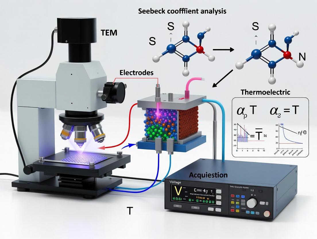
This article explores the transformative methodology of in situ Transmission Electron Microscopy (TEM) for measuring the Seebeck coefficient and other thermoelectric properties at the nanoscale.
In Situ TEM for Seebeck Coefficient Measurement: A Revolutionary Approach for Nanoscale Thermoelectric Characterization
Abstract
This article explores the transformative methodology of in situ Transmission Electron Microscopy (TEM) for measuring the Seebeck coefficient and other thermoelectric properties at the nanoscale. It details the foundational principles of integrating microelectromechanical systems (MEMS) chips within TEM to apply thermal gradients and measure resultant thermovoltages in real-time. The content covers the complete workflow from custom MEMS chip design and sample preparation via Focused Ion Beam (FIB) to the correlation of atomic-scale structural data with thermoelectric performance. It further addresses critical challenges such as electron-beam sensitivity and quantitative calibration, while comparing this technique against conventional methods. Aimed at researchers and scientists in materials science and engineering, this guide provides a comprehensive resource for leveraging in situ TEM to unlock profound insights into the structure-property relationships of next-generation thermoelectric materials.
The 'Why': Foundations of In-Situ TEM for Thermoelectric Analysis
The pursuit of higher efficiency in thermoelectric energy conversion necessitates a fundamental shift from characterizing bulk material properties to understanding local nanoscale phenomena. Global challenges in energy efficiency have positioned thermoelectric energy conversion as a pivotal research frontier, particularly for its potential to transform low-grade thermal energy into usable electricity [1]. The performance of thermoelectrics is quantified by the dimensionless figure of merit, zT, which depends on the Seebeck coefficient, electrical conductivity, and thermal conductivity [1]. These properties are fundamentally governed by microstructural features including grain boundaries, dopants, and crystal defects. While bulk measurements provide averaged properties, they obscure the individual contributions of these nanoscale features. In-situ transmission electron microscopy (TEM) emerges as a transformative approach that enables direct correlation of nanoscale structure with locally measured thermoelectric properties, bridging a critical gap in materials characterization [2] [1].
Principles of In-Situ TEM Thermoelectric Characterization
Fundamental Thermoelectric Parameters
The efficiency of thermoelectric materials is governed by several interconnected parameters that can be quantified at the nanoscale:
Seebeck Coefficient (S): Defined as the ratio of the generated thermovoltage (ΔV) to the applied temperature difference (ΔT), expressed as S = ΔV/ΔT [1]. This parameter indicates the magnitude of voltage generated per degree of temperature difference across a material.
Electrical Conductivity (σ): Calculated using the formula σ = IL/(ΔVA), where I represents current, L denotes probe spacing, A is the cross-sectional area of the sample, and ΔV is the potential difference [1].
Thermal Conductivity (κ): Comprises electronic (κ~E~) and lattice (κ~L~) components, with strategic approaches including alloying, nanostructuring, and defect engineering effectively suppressing thermal transport by promoting phonon scattering [1].
Dimensionless Figure of Merit (zT): The comprehensive metric for thermoelectric performance defined as zT = S²σT/(κ~E~ + κ~L~), where T is the absolute temperature [1].
Advantages of Nanoscale Characterization
In-situ TEM characterization provides unique capabilities beyond bulk measurement approaches:
Direct Structure-Property Correlation: Enables direct correlation of thermoelectric properties with structural and chemical composition at the atomic level, including grain boundaries, dopants, or crystal defects [2] [1].
Dynamic Evolution Tracking: Facilitates real-time observation of property changes during heating or electrical current application, allowing researchers to track dynamic evolution under operational conditions [2] [1].
Localized Property Mapping: Reveals property variations across different microstructural features that are averaged out in bulk measurements, providing insights into individual contributions of defects, interfaces, and phases [2].
High Spatial Resolution: Leverages TEM's unparalleled spatial resolution and comprehensive analytical versatility to establish precise structure-property correlations [1].
Experimental Setup and Microchip Design
MEMS-Based In-Situ TEM Chips
Custom micro-electromechanical systems (MEMS) chips form the foundation of in-situ TEM thermoelectric characterization:
Figure 1: MEMS Chip Architecture for In-Situ TEM Thermoelectric Characterization
Advanced Characterization Techniques Integration
The experimental setup integrates multiple advanced electron microscopy techniques:
Four-Dimensional Scanning Transmission Electron Microscopy (4D-STEM): Utilizes a convergent electron beam that scans the sample point-by-point, collecting diffraction patterns to form a comprehensive dataset for ptychography, enabling precise structural analysis of beam-sensitive materials [1].
Electron Energy Loss Spectroscopy (EELS): Employed with high energy resolution to investigate phonon dispersion relationships of defects, providing crucial insights into thermal conductivity and phonon-electron interactions at the nanoscale [1].
Cryogenic Electron Microscopy (Cryo-EM): Implemented using cryo-holders or aberration-corrected electron microscopy equipped with cooling systems to analyze thermally sensitive samples such as fast ion conductors (e.g., Ag~2~S, Ag~2~Se), minimizing radiation damage [1].
Annular Bright Field and Integrated Differential Phase Contrast: Aberration-corrected techniques that facilitate simultaneous imaging of light and heavy atoms, providing enhanced contrast for comprehensive defect analysis [1].
Application Notes and Experimental Protocols
Protocol 1: Seebeck Coefficient Measurement of Nanowires
Objective: Quantify the Seebeck coefficient of individual thermoelectric nanowires with simultaneous structural characterization.
Materials and Equipment:
- In-situ TEM holder with thermal and electrical biasing capabilities
- MEMS chip with integrated heating elements and electrical contacts
- Synthesized thermoelectric nanowires (e.g., Bi~2~Te~3~, Sb~2~Te~3~)
- Nanomanipulation system for sample transfer
- FIB-SEM system for sample preparation
Procedure:
Sample Preparation (Duration: 4-6 hours)
- Transfer individual nanowires onto the MEMS chip using nanomanipulators
- Establish electrical contacts using electron-beam-induced deposition (EBID) of Pt
- Verify contact quality through I-V characterization within TEM
- Record initial structural state using HRTEM and selected area electron diffraction
Temperature Gradient Calibration (Duration: 1-2 hours)
- Activate differential heating elements to establish controlled temperature gradient
- Calibrate local temperature using temperature-dependent material properties
- Measure actual temperature distribution using nanoscale thermometry methods
- Optimize ΔT to achieve 5-50K range across the nanowire
Thermovoltage Measurement (Duration: 30-60 minutes)
- Apply stabilized temperature gradient across the nanowire
- Measure induced thermovoltage using high-impedance voltmeter
- Record simultaneous structural evolution during measurement
- Repeat measurements at different average temperatures (25°C-200°C)
Data Analysis and Validation
- Calculate Seebeck coefficient using S = ΔV/ΔT
- Correlate measured values with observed microstructure
- Compare with bulk measurements for validation
- Perform statistical analysis across multiple nanowires
Troubleshooting Tips:
- Poor electrical contacts: Increase EBID deposition time and verify connectivity
- Unstable temperature gradient: Verify heater calibration and contact thermal resistance
- Sample drift during measurement: Implement drift correction algorithms
- Contamination: Use cryogenic cooling or local heating to reduce hydrocarbon deposition
Protocol 2: Dynamic Crystallization of Amorphous Thin Films
Objective: Track thermoelectric property evolution during in-situ crystallization of amorphous germanium thin films.
Materials and Equipment:
- Amorphous germanium thin films (50-200 nm thickness)
- MEMS chip with precision heating capability
- In-situ TEM holder with thermal control
- High-speed camera for recording transformation
Procedure:
Initial Characterization (Duration: 1 hour)
- Acquire bright-field and dark-field TEM images of amorphous structure
- Perform electron diffraction to confirm amorphous nature
- Establish baseline electrical conductivity and thermovoltage
Progressive Crystallization (Duration: 2-3 hours)
- Apply controlled heating ramp (2-5°C/min) from 25°C to 450°C
- Continuously monitor thermovoltage during heating
- Record selected area diffraction patterns at 30-second intervals
- Capture high-resolution images at critical transformation stages
Multi-Point Property Correlation
- Correlate specific structural transformations with thermovoltage changes
- Identify nucleation sites and track grain growth
- Measure property differences between amorphous and crystalline regions
- Quantify interface effects on thermoelectric properties
Key Observations:
- Thermoelectric voltage tracks directly with crystallization progress [2]
- Significant property changes occur at specific crystallization stages
- Interface-dominated transport mechanisms become apparent
- Defect formation during crystallization impacts electronic transport
Quantitative Data Acquisition and Analysis
Table 1: Thermoelectric Property Measurement Parameters and Techniques
| Parameter | Measurement Technique | Typical Range | Accuracy | Special Considerations |
|---|---|---|---|---|
| Seebeck Coefficient (S) | Differential thermovoltage measurement | 10-1000 μV/K | ±5% | Requires stable ΔT, minimized parasitic EMF |
| Electrical Conductivity (σ) | Four-point probe method | 10-10^5^ S/m | ±10% | Contact resistance compensation, geometry factors |
| Temperature Gradient (ΔT) | Differential heating, nanothermometry | 1-100 K | ±0.5 K | Spatial resolution limitations, calibration critical |
| Thermal Conductivity (κ) | Bridge method, Raman thermometry | 0.1-100 W/mK | ±15% | Challenging direct measurement, often calculated |
| Dimensionless Figure of Merit (zT) | Combined measurements | 0.1-2.5 | ±20% | Requires multiple independent measurements |
Research Reagent Solutions and Essential Materials
Table 2: Essential Materials for In-Situ TEM Thermoelectric Characterization
| Material/Category | Specific Examples | Function/Purpose | Key Characteristics |
|---|---|---|---|
| MEMS Chips | Custom in-situ TEM microchips with heating capabilities | Platform for nanomaterial testing, temperature gradient generation | Integrated heating elements, electrical contacts, temperature sensors [2] [1] |
| Thermoelectric Nanomaterials | Bi~2~Te~3~ nanowires, Sb~2~Te~3~ films, Ge thin films | Primary test materials for property characterization | Controlled composition, defined geometry, specific crystal structure [2] |
| Contact Materials | Electron-beam induced Pt/Ga deposits, focused ion beam (FIB) Pt | Establishing electrical connections to nanomaterials | High conductivity, stability under electron beam, minimal interface resistance [1] |
| Calibration Standards | Known thermoelectric materials (Bulk Bi~2~Te~3~, Sb~2~Te~3~) | Validation of measurement accuracy | Certified property values, stability, reference measurements [2] |
| Beam-Sensitive Material Supports | Cryo-holders, low-dose imaging supports | Analysis of delicate materials (Ag~2~S, Ag~2~Se) | Radiation damage mitigation, temperature control [1] |
Data Interpretation and Analysis Framework
Workflow for Correlative Analysis
Figure 2: Workflow for Correlative Structure-Property Analysis
Advanced Analytical Techniques
4D-EELS for Phonon Dispersion: Experimental setup with slot aperture placed parallel to interfaces produces dispersion diagrams along high-symmetry directions, enabling fundamental understanding of thermal conductivity and phonon-electron interactions at the nanoscale [1].
4D-STEM Ptychography: Convergent electron beam scanning with collection of diffraction patterns forms a comprehensive 4D dataset, particularly valuable for electron-beam-sensitive materials that require minimal dose imaging [1].
Tomography Techniques: Enable three-dimensional visualization of defect structures, providing comprehensive understanding of complex microstructural networks and their impact on thermoelectric transport properties [1].
The integration of in-situ TEM characterization with thermoelectric measurements represents a paradigm shift in materials research, enabling unprecedented insights into structure-property relationships at the nanoscale. Current capabilities for semi-quantitative characterization are rapidly evolving toward full quantitative measurement of temperature gradients, electrical and thermal conductivities, and Seebeck coefficients [2]. The ongoing development of improved in-situ TEM microchip designs promises enhanced measurement precision and expanded experimental capabilities [2].
The true power of this approach lies in its ability to directly correlate thermoelectric properties with structural and chemical composition across multiple scales - from atomic-level defects to microstructural features - while simultaneously tracking dynamic evolution during heating or electrical current application [2] [1]. This correlative methodology enables researchers to move beyond ensemble-averaged properties and understand the individual contributions of specific defects, interfaces, and phases to overall thermoelectric performance.
As these techniques continue to mature, they will undoubtedly accelerate the rational design of next-generation thermoelectric materials with optimized performance characteristics and enhanced operational durability. The bridging of the gap between bulk measurements and nanoscale property analysis marks a critical advancement in our fundamental understanding of thermoelectric phenomena and our practical ability to engineer materials for superior energy conversion efficiency.
The pursuit of high-efficiency thermoelectric materials, which can directly convert heat into electrical energy, hinges on our ability to understand and optimize their fundamental properties. Central to this effort is the Seebeck coefficient (S), a material-specific parameter that quantifies the magnitude of an induced thermovoltage in response to an applied temperature gradient. For decades, the measurement of this property and the interpretation of its underlying mechanisms were confined to the macroscopic scale. However, the emergence of in-situ Transmission Electron Microscopy (TEM) has fundamentally altered this landscape by creating a novel synergy with the Seebeck effect. This synergy enables researchers to directly correlate a material's thermoelectric performance with its atomic-scale structure and composition—including defects, grain boundaries, and dopants—under dynamic operational conditions [1] [2]. This application note details the protocols and methodologies underpinning this powerful combination, providing a framework for its application in advanced thermoelectric materials research.
Fundamental Principles and Theoretical Background
The Seebeck Effect in Thermoelectricity
The Seebeck effect is the cornerstone of thermoelectric energy conversion. It describes the phenomenon where a temperature difference (∆T) across a material results in a measurable electrical potential difference (∆V). The Seebeck coefficient (S) is defined as: [ S = -\frac{\Delta V}{\Delta T} ] This coefficient, alongside electrical conductivity (σ) and thermal conductivity (κ), determines the thermoelectric figure of merit, zT = (S²σT)/κ, which defines the overall efficiency of a thermoelectric material [3]. A high zT is essential for practical applications, and achieving it requires a delicate balance: a high Seebeck coefficient and high electrical conductivity must be maintained while simultaneously suppressing thermal conductivity [4]. The Seebeck coefficient is profoundly sensitive to a material's electronic structure, as well as micro- and atomic-scale features such as dopants, impurities, and crystallinity, making its accurate measurement and interpretation at relevant scales critical [5].
The Role of Advanced Electron Microscopy
Electron microscopy provides the spatial resolution necessary to probe the structural origins of thermoelectric properties. Modern TEM techniques offer unparalleled capabilities:
- High-Resolution TEM (HRTEM): Directly images defect types including dislocations, grain boundaries, and precipitates [1].
- Spectroscopic Techniques: Energy Dispersive X-ray Spectroscopy (EDS) and Electron Energy Loss Spectroscopy (EELS) provide comprehensive data on elemental distribution, chemical shifts, and bonding [1].
- 4D-STEM Ptychography: Enables high-resolution imaging of electron-beam-sensitive materials by collecting full diffraction patterns at each scan point [1].
- Cryogenic EM (cryo-EM): Minimizes beam damage for sensitive materials like fast ion conductors (e.g., Ag₂S, Ag₂Se), preserving their native state for analysis [1].
The integration of these techniques allows for the establishment of definitive structure-property correlations. For instance, EELS with high energy resolution can be employed to investigate phonon dispersion at defects, which directly influences thermal conductivity—a key parameter in the zT equation [1].
Experimental Protocols for In-Situ TEM Seebeck Coefficient Measurement
This protocol outlines the procedure for performing a semi-quantitative measurement of the Seebeck coefficient within a Transmission Electron Microscope using a custom Micro-Electrochemical Systems (MEMS) chip.
Materials and Equipment
Table 1: Essential Research Reagents and Equipment
| Item | Function / Description | Key Considerations |
|---|---|---|
| In-Situ TEM Chip | Custom MEMS device with integrated heating elements and electrical contacts [2]. | Must feature a differential heating device and multiple contact pads on a silicon nitride membrane. |
| Bulk or Nanomaterial Samples | The material under investigation (e.g., p-doped Si, Mo, Ca₃Co₄O₉, Ge thin films) [5]. | Sample must be electron-transparent for TEM imaging. |
| Focused Ion Beam (FIB) System | Used for site-specific sample preparation and deposition onto the MEMS chip [5]. | Critical for creating devices with defined geometry from bulk materials or manipulating nanotubes. |
| Transmission Electron Microscope | Provides the platform for simultaneous structural/chemical analysis and in-situ electrical biasing. | Should be equipped with EDS and EELS capabilities for comprehensive analysis. |
| Source Measure Units (SMUs) | Precision instruments for applying heating current (IH) and measuring the resulting voltage (∆V) [5]. | Required for sensitive I-V characterization and thermovoltage measurement. |
Step-by-Step Methodology
Step 1: Device Fabrication and Sample Transfer
- Chip Design: Utilize a MEMS chip featuring a free-standing silicon nitride membrane (e.g., 1 µm thick). A differential heating device should be positioned to one side, with two or more contact pads (e.g., 10 nm Ti / 150 nm Pt) located in the membrane's center [5].
- Sample Preparation: For bulk materials, use the FIB to lift out a micro-scale cuboid of the material and deposit it across the two contact pads, thinning the central region to electron transparency. For nanomaterials (e.g., nanotubes), transfer and position individual structures using a nanomanipulator within the FIB [5].
Step 2: Experimental Setup and Calibration
- Insert the prepared MEMS chip into a dedicated in-situ TEM holder with electrical biasing capabilities.
- Establish electrical connections to the chip's heating element and the sample's contact pads.
- Perform an initial I-V characterization of the sample at zero heating current (IH = 0) to determine the baseline device resistance and check for proper electrical contact [5].
Step 3: Generation of Temperature Gradient and Data Acquisition
- Apply a controlled heating current (IH) to the differential heating element. This creates a temperature gradient (∆T) along the sample.
- Simultaneously, perform I-V measurements on the sample across a range of applied voltages at each fixed IH value. The I-V curve will exhibit a voltage offset (V₀) relative to the IH=0 curve due to the generated thermovoltage [5].
- For each I-V curve, perform a linear regression, I(V) = -V/R + I₀, and calculate the voltage offset as V₀ = -I₀R. The Seebeck voltage is then ∆V = V₀(IH) - V₀(0) [5].
Step 4: Structural and Chemical Correlation
- While applying IH and measuring ∆V, use TEM imaging, SAED, EDS, and/or EELS to characterize the sample's crystal structure, defect density, grain boundaries, and chemical composition in the exact region where the thermoelectric measurement is occurring [2] [5].
Step 5: Data Analysis and Validation
- The sign of the measured ∆V corresponds directly to the sign of the material's Seebeck coefficient [2] [5].
- For a fully quantitative measurement of S, an independent and accurate measurement of the temperature gradient (∆T) along the sample is required, which remains a primary challenge. Current studies are often semi-quantitative, demonstrating proof-of-concept and relative comparisons [2] [5].
- Correlate trends in the measured ∆V with observed structural features, such as changes during the crystallization of an amorphous film or the presence of specific grain boundaries [2].
The workflow for this integrated measurement is summarized below.
Data Presentation and Analysis
Quantitative Measurement Data
The following table synthesizes representative data from in-situ TEM thermoelectric studies, illustrating the type of quantitative information that can be derived.
Table 2: Representative Data from In-Situ TEM Thermoelectric Characterization
| Material System | Measured Signal / Property | Key Quantitative Observation | Structural Correlation |
|---|---|---|---|
| p-doped Si [5] | Voltage Offset (V₀) | V₀ increased positively with IH, from ~0 mV (IH=0) to >5 mV (IH=5 mA). | Positive sign of V₀ agreed with known positive S of p-Si. Minor Ga implantation from FIB noted via EDS. |
| Molybdenum (Mo) [5] | Voltage Offset (V₀) | V₀ increased positively with IH. | Positive sign of V₀ agreed with known positive S of Mo. |
| Amorphous Ge Thin Film [2] | Thermovoltage (∆V) | Tracking of ∆V during in-situ crystallization. | Direct correlation established between evolving thermovoltage and the microstructural transformation from amorphous to crystalline phase. |
| Ca₃Co₄O₉ (CCO) MLC [5] | Voltage Offset (V₀) & Crystallographic Orientation | Compared V₀ for two device orientations: current flow parallel (CCO∥) and perpendicular (CCO⟂) to the MLC layers. | SAED confirmed orientation. Thermovoltage signal was successfully measured for both anisotropic configurations. |
| Standard Measurement Protocol [6] | Seebeck Coefficient (S) | Identified that off-axis 4-probe contact geometry leads to greater local temperature measurement error vs. 2-probe, overestimating S. | Error arises from higher macroconstriction and contact resistance, exacerbated at high temperatures. |
Visualizing the Measurement Principle
The core principle of generating and measuring a thermovoltage within the TEM is illustrated in the following diagram.
Application Notes and Technical Considerations
Advantages and Unique Capabilities
- Direct Structure-Property Correlation: The primary advantage is the ability to link measured thermoelectric signals (e.g., ∆V) directly to atomic-scale structural features such as grain boundaries, dislocations, and dopant atoms observed in real-time [2] [5].
- Dynamic Evolution Studies: This approach allows for the tracking of property changes during phase transitions, crystallization, or under applied electrical stress, providing insights into degradation mechanisms and operational stability [2].
- Analysis of Individual Nanostructures: It enables the characterization of single nanotubes, nanowires, or other nanoscale objects, which is often challenging with bulk measurement techniques [5].
Limitations and Challenges
- Quantification of ΔT: A significant challenge is the accurate and direct measurement of the local temperature gradient (∆T) across the nanomaterial. Current methods often rely on modeling or calibration, limiting fully quantitative analysis [2].
- Sample Preparation Complexity: FIB-based transfer and thinning are complex, time-consuming, and can introduce defects (e.g., Ga implantation) or stress that may alter the material's intrinsic properties [5].
- Electron Beam Effects: The high-energy electron beam can cause heating, radiolysis, or knock-on damage in sensitive materials, potentially modifying the structure being observed. Techniques like cryo-EM or low-dose 4D-STEM are required to mitigate this [1].
Future Outlook and Protocol Evolution
The field is rapidly advancing toward fully quantitative and less invasive characterization. Promising directions include:
- Improved Chip Design: Next-generation MEMS chips with integrated, localized temperature sensors (e.g., nanothermocouples) are proposed to directly measure ∆T, enabling accurate calculation of S [2] [5].
- Integration of Advanced Techniques: Combining in-situ biasing with high-energy resolution EELS for phonon studies and ptychographic imaging will provide a more complete picture of electronic, thermal, and structural dynamics [1].
- Cryogenic Workflows: Wider adoption of cryo-EM holders and protocols will be essential for characterizing highly beam-sensitive thermoelectric materials, such as fast ion conductors, without introducing artifacts [1].
The pursuit of advanced thermoelectric (TE) materials demands a profound understanding of the fundamental relationships between atomic-scale structure and macroscopic TE properties. In situ transmission electron microscopy (TEM) has emerged as a transformative methodology that enables direct correlation of atomic structure, chemical composition, and thermoelectric function within a single experimental platform. This approach allows researchers to track the dynamic evolution of TE properties during material synthesis, phase transitions, and under operational conditions, providing unprecedented insights into structure-property relationships that govern TE performance [2]. The capability to perform simultaneous structural characterization and functional property measurement represents a paradigm shift in thermoelectric materials research, moving beyond traditional ex situ methods that require separate structural and property analyses.
The core advantage of in situ TEM techniques lies in their ability to bridge the critical knowledge gap between theoretical predictions and experimental observations. By applying controlled temperature gradients and measuring resulting thermovoltages while simultaneously imaging the material structure down to atomic resolution, researchers can directly observe how specific structural features—including grain boundaries, crystal defects, dopant distributions, and interfacial structures—impact charge and heat transport phenomena [2]. This integrated characterization approach is particularly valuable for understanding complex TE material systems where performance is optimized through strategic nanostructuring and defect engineering to enhance the Seebeck coefficient while minimizing thermal conductivity.
Experimental Protocols for In Situ TEM Thermoelectric Characterization
Microchip-Based Measurement Platform
The foundation of in situ TEM thermoelectric characterization involves specialized microchips that integrate heating elements and electrical measurement capabilities. The following protocol details the setup and operation:
Microchip Preparation and Mounting: Utilize a custom-designed in situ TEM microchip featuring a differential heating element capable of generating controlled temperature gradients across the specimen. The microchip should be mounted in a specialized TEM holder with electrical contacts for both heating and measurement functions. Ensure the holder provides at least four electrical contacts: two for passing current through the heating element and two for measuring the resulting thermovoltage across the sample [2].
Sample Transfer and Device Fabrication: For nanomaterial specimens, transfer the material onto the microchip using nanomanipulation systems. For thin-film specimens, utilize focused ion beam (FIB) milling to prepare lamellae and weld them to the electrical contacts via electron-beam-induced deposition of platinum or tungsten. Critical: Ensure the sample forms a complete electrical circuit between the measurement electrodes while being suspended across the temperature gradient zone [2].
Temperature Gradient Calibration: Activate the differential heating element to establish a temperature gradient (ΔT) across the sample. Quantify the actual temperature values at both hot and cold ends using calibrated temperature-dependent features such as material phase transition points or resistivity changes in reference materials. For semi-quantitative studies, the exact temperature values may be estimated based on input power and finite element simulations, though full quantitative measurements require improved chip designs with integrated nanothermometers [2].
Simultaneous Structural and Electrical Characterization: With an established temperature gradient, acquire high-resolution TEM (HRTEM), scanning TEM (STEM), or electron energy loss spectroscopy (EELS) data to characterize the atomic structure and composition while simultaneously measuring the open-circuit voltage (thermovoltage, VTE) generated across the sample. The sign of VTE directly corresponds to the sign of the sample's Seebeck coefficient [2].
Dynamic Evolution Studies: For time-dependent processes such as crystallization, phase transitions, or defect migration, track changes in VTE while recording structural evolution through video-rate TEM or time-series image acquisition. This approach was successfully demonstrated during in situ crystallization of amorphous Ge thin films, where the thermovoltage evolution directly correlated with the progression of crystallization [2].
Data Correlation and Analysis: Correlate specific structural features observed in TEM images (grain boundaries, interfaces, defects) with localized changes in thermoelectric response. Calculate the Seebeck coefficient as S = -VTE/ΔT, where ΔT is the calibrated temperature difference across the sample.
Advanced Protocol: Atomic-Resolution Interfacial Analysis in TE Nanocomposites
This specialized protocol focuses on characterizing heterogeneous interfaces in TE nanocomposites, which significantly impact both electronic and thermal transport:
Nanocomposite Synthesis: Incorporate second-phase nanoparticles (e.g., magnetocaloric LaFeSi nanoparticles in BiSbTe matrix) using spark plasma sintering (SPS) method. Vary the nanoparticle concentration (e.g., x = 0.1%, 0.2%, 0.3%, 0.4%) to optimize TE performance [7].
Cross-sectional Sample Preparation: Prepare electron-transparent cross-sections of the nanocomposite interface using FIB milling with final low-energy ion polishing to minimize surface damage.
Atomic-Resolution STEM Imaging: Acquire atomic-resolution high-angle annular dark-field (HAADF)-STEM images of the nanoparticle-matrix interface. Use aberration-corrected STEM for optimal resolution.
Spectroscopic Characterization: Perform energy-dispersive X-ray spectroscopy (EDS) and electron energy loss spectroscopy (EELS) line scans across the interface to quantify elemental interdiffusion and identify interfacial reaction products.
Defect Analysis: Identify and characterize interfacial defects, vacancies, and strain fields using geometric phase analysis (GPA) of HRTEM images. In BiSbTe/LaFeSi nanocomposites, this approach revealed that Te vacancies originating from interfacial reaction decrease hole concentration and enhance the Seebeck coefficient [7].
Property Correlation: Correlate specific interfacial structures with macroscopic TE properties measured separately, establishing structure-property relationships. For example, interfaces and defects enhance phonon scattering, reducing thermal conductivity while appropriate interfacial chemistry optimizes electronic transport [7].
Data Presentation and Analysis
Quantitative Thermoelectric Performance Data
Table 1: Thermoelectric performance of selected materials systems characterized through in situ and theoretical methods.
| Material System | Seebeck Coefficient (μV/K) | ZT Value | Temperature (K) | Key Structural Feature | Characterization Method |
|---|---|---|---|---|---|
| Ge1Sb6Te10 (GST-I stacking) | Not specified | 2.23 (max) | 710 | 51-layer trigonal structure | DFT calculation [8] |
| Ge1Sb6Te10 (GST-II stacking) | Not specified | 1.91 (max) | 710 | Alternative atomic stacking | DFT calculation [8] |
| 0.2% LFS/BST Nanocomposite | Enhanced vs. matrix | 1.11 | 380 | Te vacancies at interface | Experimental measurement [7] |
| Bi₀․₃Sb₁․₇Te₃ (BST matrix) | Reference | 0.94 (at 380K) | 380 | Baseline material | Experimental measurement [7] |
Structural Properties and Thermal Conductivity
Table 2: Structural characteristics and thermal transport properties of Ge1Sb6Te10 with different atomic stackings.
| Atomic Stacking | Crystal Structure | Electronic Behavior | Lattice Thermal Conductivity (W/m·K at 300K) | Stability |
|---|---|---|---|---|
| GST-I | Trigonal (R̅3m), 51-layer | Semiconductor | 0.86 | Experimentally confirmed [8] |
| GST-II | Trigonal (R̅3m), 51-layer | Semiconductor | 0.78 | Theoretical prediction [8] |
| GST-III | Trigonal (R̅3m), 51-layer | Not specified | Not specified | Experimentally confirmed [8] |
| GST-IV | Trigonal (R̅3m), 51-layer | Semi-metallic | Not specified | Theoretical prediction [8] |
Visualization of Methodologies and Relationships
Experimental Workflow for In Situ TEM Thermoelectric Characterization
Structure-Property Relationships in Thermoelectric Materials
The Scientist's Toolkit: Essential Research Reagents and Materials
Table 3: Key research reagents, materials, and equipment for in situ TEM thermoelectric characterization.
| Item | Function/Application | Specific Examples |
|---|---|---|
| Custom TEM Microchips | Generate temperature gradients and enable electrical measurements | Differential heating elements for ΔT creation [2] |
| Phase Change Materials | Model systems for structure-property studies | GeTe-Sb₂Te₃ pseudobinary alloys (GST) [8] |
| Nanocomposite Systems | Study interface effects on TE properties | BiSbTe with LaFeSi nanoparticles [7] |
| DFT Calculation Platforms | Predict atomic structure and transport properties | ALKEMIE platform with automated workflows [8] |
| Advanced TEM Techniques | Atomic-resolution structure and composition analysis | HAADF-STEM, EELS, EDS [7] |
| Transport Property Calculations | Model electronic and thermal transport | BoltzTraP (electronic), ShengBTE (thermal) [8] |
The correlation of atomic structure, composition, and thermoelectric function through in situ TEM methodologies represents a powerful approach for advancing TE materials research. The key advantages of this integrated characterization strategy include the direct visualization of structure-property relationships at relevant length scales, the ability to track dynamic evolution during phase transitions, and the capability to quantify how specific defects and interfaces impact both electronic and thermal transport. Future developments in microchip design, including integrated nanothermometers for quantitative temperature gradient measurement, will further enhance the quantitative capabilities of this technique [2]. As these methodologies continue to evolve, they will accelerate the discovery and optimization of next-generation thermoelectric materials with enhanced performance for energy harvesting and solid-state cooling applications.
In-situ Transmission Electron Microscopy (TEM) thermoelectric characterization represents a cutting-edge frontier in materials science, enabling the direct correlation of a material's atomic-scale structure with its functional thermoelectric properties. This technique allows researchers to observe dynamic processes such as crystallization, defect migration, and phase transitions while simultaneously quantifying key thermoelectric parameters. The core principle involves generating a controlled temperature gradient across a nanoscale specimen within the TEM and measuring the resulting electrical response, primarily the thermovoltage from which the Seebeck coefficient can be derived. By integrating microelectromechanical systems (MEMS) technology with electron microscopy, this approach provides unprecedented insights into structure-property relationships in thermoelectric materials, from bulk semiconductors to low-dimensional nanomaterials [2] [1]. The following sections detail the essential components, experimental protocols, and analytical methods required to implement this powerful characterization technique.
Core Components of the Experimental Setup
MEMS-Based In-Situ TEM Microchip
The specialized MEMS microchip serves as the foundational platform for in-situ thermoelectric experiments. These chips typically feature a free-standing low-stress silicon nitride membrane (approximately 1 μm thick) that provides mechanical support while allowing electron transparency for TEM imaging [5]. The active components include:
- Differential Heating Element: A microfabricated heater located on one side of the membrane creates a controlled temperature gradient when current is applied [2] [5].
- Electrical Contact Pads: Metallic electrodes (typically 10 nm Ti + 150 nm Pt) are patterned on the membrane to simultaneously measure electrical properties while applying thermal stimuli [5].
- Temperature Sensors: Integrated sensors enable real-time monitoring and calibration of local temperatures across the device [1].
Advanced chip designs may incorporate multiple independent heating elements and up to eight electrical contacts to enable more complex measurement configurations, including four-point probe electrical characterization [1].
TEM Holder and System Integration
The MEMS chip interfaces with the transmission electron microscope through a specialized holder system that delivers both electrical signals and thermal management. Commercial systems (e.g., Protochips Fusion AX) provide precision control over temperature (room temperature to 1200°C) and electrical parameters (with resolution down to picoamps) while maintaining compatibility with high-resolution TEM imaging [9]. Key requirements include:
- Friction-free double tilting capabilities for crystallographic orientation
- Electrical isolation to minimize noise during sensitive measurements
- Thermal stability to reduce specimen drift during acquisition
- Integration with microscope control systems for synchronized data collection
Sample Preparation Subsystems
Preparation of specimens for in-situ TEM thermoelectric studies requires specialized equipment:
- Focused Ion Beam (FIB) System: Essential for site-specific extraction and thinning of bulk materials or individual nanostructures [5].
- Nanomanipulation Tools: For precise transfer and positioning of nanomaterials (e.g., nanotubes, nanowires) onto the MEMS chip contacts [5].
- Metallic Coating Capability: For non-conductive samples, a thin metal coating (e.g., iridium, gold) is applied to ensure electrical conductivity while minimizing thermal mass [10].
Experimental Protocols and Methodologies
Device Preparation and Installation
Table 1: Sample Preparation Methods for Different Material Forms
| Material Type | Preparation Method | Key Considerations | Reference |
|---|---|---|---|
| Bulk Materials | FIB milling to create cuboid structures with defined geometry | Control crystal orientation relative to temperature gradient; Minimize Ga+ implantation and surface oxidation | [5] |
| Nanotubes/Nanowires | Transfer via nanomanipulation | Ensure secure electrical contact at both ends; Minimize contact resistance | [5] |
| Thin Films | Direct deposition or FIB transfer | Control thickness for electron transparency; Characterize initial crystallinity | [2] |
| Non-conductive Materials | Sputter coating with thin metal layer (Ir, Au) | Optimize coating thickness (~10-50 nm) for conductivity while minimizing thermal influence | [10] |
- MEMS Chip Preparation: Clean the microchip to remove contaminants that could interfere with electrical measurements or sample adhesion.
- Sample Transfer: Using FIB or nanomanipulation, transfer the material of interest to bridge the two contact pads on the MEMS chip [5].
- Structural Verification: Before in-situ experiments, characterize the initial microstructure, crystallinity, and composition using standard TEM techniques (SAED, HRTEM, EDX) [5].
Thermoelectric Measurement Protocol
Establish Baseline Conditions:
- Acquire reference structural images and diffraction patterns at room temperature without applied heating current.
- Perform initial I-V characterization at IH = 0 to determine sample resistance and contact quality [5].
Apply Temperature Gradient:
- Incrementally increase the heating current (IH) to the differential heating element to establish a controlled temperature gradient along the sample.
- Record the corresponding temperature values from integrated sensors if available [2].
Simultaneous Electrical and Structural Characterization:
- For each heating current step, acquire I-V curves while monitoring structural evolution.
- Measure the voltage offset (V0) resulting from the temperature gradient using linear regression of I-V curves: I(V) = -V/R + I0, with V0 = -I0R [5].
- Track dynamic processes (e.g., crystallization, phase transitions) through correlated imaging and electrical measurement.
Data Acquisition and Synchronization:
- Utilize machine vision software (e.g., AXON platform) to synchronize TEM imaging with thermal and electrical parameter recording [9].
- Implement live physical drift correction to maintain region of interest during thermal expansion.
- Record all parameters (TEM magnification, camera settings, heating currents, voltages) in an indexed database for post-processing [9].
Quantitative Analysis Methods
The voltage offset (V0) measured at different heating currents provides the fundamental data for determining the Seebeck coefficient. For quantitative analysis:
Seebeck Coefficient Calculation: The Seebeck coefficient (S) is determined from the relationship S = ΔV/ΔT, where ΔV is the measured thermovoltage and ΔT is the temperature difference along the sample [1].
Electrical Conductivity Determination: Electrical conductivity (σ) is calculated using the formula σ = IL/(ΔVA), where L represents the probe spacing, A denotes the cross-sectional area of the sample, I is the current, and ΔV is the potential difference [1].
Temperature Gradient Calibration: Accurate quantification requires calibration of the actual temperature gradient, which can be achieved through:
- Finite element modeling of thermal distribution in the MEMS device
- Reference measurements with materials of known Seebeck coefficient
- Direct measurement using integrated nanothermometers [2]
The Scientist's Toolkit: Essential Research Reagents and Materials
Table 2: Essential Materials and Reagents for In-Situ TEM Thermoelectric Experiments
| Item | Function/Purpose | Specifications/Considerations |
|---|---|---|
| MEMS Microchips | Platform for in-situ measurements | Low-stress SiN membrane (1 μm); Pt/Ti electrodes; Integrated heaters & sensors [5] [9] |
| Reference Materials | Calibration and validation | p-doped Si, Mo, standard thermoelectrics with known Seebeck coefficients [5] |
| FIB Deposition Materials | Sample preparation and fixing | Pt, W, or C for site-specific deposition and attachment [5] |
| Sputter Coating Materials | Rendering non-conductive samples measurable | Ir, Au (10-50 nm thickness) for electrical conductivity without significant thermal influence [10] |
| Calibration Standards | Temperature sensor calibration | Materials with known phase transition temperatures for temperature gradient verification |
Advanced Techniques and Correlative Approaches
The integration of complementary characterization techniques significantly enhances the information obtained from in-situ TEM thermoelectric experiments:
4D-STEM Ptychography: Enables mapping of strain fields, electric fields, and charge distribution under operational conditions, providing insight into how local structure affects thermoelectric performance [1].
Electron Energy Loss Spectroscopy (EELS): High energy resolution EELS can investigate phonon dispersion relationships at defects and interfaces, crucial for understanding thermal conductivity and electron-phonon interactions [1].
Cryogenic Techniques: For thermally sensitive materials (e.g., fast ion conductors), cryo-EM preserves native structures while enabling thermoelectric characterization [1].
Tomographic Integration: Intermittent heating and cooling during tilt-series acquisition enables 4D (space and time) observation of structural evolution under thermal stress [11].
Data Interpretation and Validation
Quantitative Analysis of Thermoelectric Parameters
Table 3: Key Parameters and Quantitative Measurements in In-Situ TEM Thermoelectric Studies
| Parameter | Measurement Method | Calculation Formula | Experimental Considerations |
|---|---|---|---|
| Seebeck Coefficient (S) | Voltage response to temperature gradient | S = ΔV/ΔT | Requires accurate ΔT measurement; Sign indicates carrier type [1] [5] |
| Electrical Conductivity (σ) | I-V characterization at each temperature | σ = IL/(ΔVA) | Requires precise geometry measurement; Contact resistance correction [1] |
| Thermal Conductivity (κ) | Combined with Raman or TDTR | κ = κE + κL | Challenging to measure directly; Often derived from modeling [2] |
| Figure of Merit (zT) | Calculated from measured parameters | zT = (S²σT)/κ | Requires all three parameters at same temperature [1] |
Correlation of Structure and Property
The unique advantage of in-situ TEM thermoelectric characterization is the direct correlation between atomic-scale structure and macroscopic properties:
- Defect-Property Relationships: Direct observation of how grain boundaries, dislocations, and precipitates affect charge and heat transport [2] [1].
- Dynamic Evolution: Tracking property changes during structural transformations, such as the crystallization of amorphous Ge thin films [2].
- Interface Effects: Characterization of interfacial resistance and its contribution to overall thermoelectric performance [5].
The essential setup for in-situ TEM thermoelectric experiments represents a powerful convergence of MEMS technology, electron microscopy, and precision electrical measurement. By implementing the components, protocols, and analysis methods described herein, researchers can achieve unprecedented insights into the fundamental relationships between atomic-scale structure and thermoelectric properties in materials. This approach enables the direct observation of dynamic processes under operational conditions, providing valuable data for the rational design of next-generation thermoelectric materials with enhanced performance characteristics.
The 'How': A Step-by-Step Guide to Method and Application
The integration of Micro-Electro-Mechanical Systems (MEMS) into experimental platforms has revolutionized materials characterization, particularly for in-situ transmission electron microscopy (TEM) investigations of thermoelectric properties. These miniaturized devices enable precise thermal and electrical manipulation of specimens under observation, allowing researchers to directly correlate a material's microstructure with its functional performance, such as the Seebeck coefficient. MEMS-based chips provide unprecedented control over experimental conditions while minimizing external interference, making them indispensable tools for advancing thermoelectric materials research. Their ability to function as both thermal sources and sensing elements within the confined space of a TEM column enables real-time observation of dynamic materials processes that was previously unattainable with conventional macroscopic testing setups.
The core advantage of MEMS platforms lies in their ability to localize thermal energy and measure properties simultaneously at the micro-scale. For Seebeck coefficient measurements, which quantify a material's ability to convert temperature gradients into electrical voltage, this simultaneous control and measurement is paramount. Modern MEMS devices achieve this through sophisticated integration of microheaters and sensors on thermally isolated membranes, permitting rapid thermal cycling with minimal power consumption—critical for prolonged in-situ experiments where stability and accuracy are paramount.
MEMS Microheater Design and Optimization
Material Selection and Configuration
The choice of materials for integrated microheaters is critical for performance and reliability, especially under the high-vacuum and high-magnification conditions of TEM. The selected materials must provide stable resistive heating, compatibility with MEMS fabrication, and withstand high-temperature operation.
Table 1: Common Materials for MEMS Microheaters and Their Properties
| Material | Typical Resistivity (Ohm-m) | Key Advantages | Application Notes |
|---|---|---|---|
| Polysilicon [12] [13] | 4 × 10⁻⁴ | High reliability at >400°C, tunable resistivity, CMOS process compatibility | Ideal for semiconductor gas sensors and as a high-temperature IR source |
| Platinum (Pt) [14] [15] | 1.06 × 10⁻⁷ | Chemically inert, stable temperature coefficient, excellent for RTDs | Used in non-magnetic heaters for atomic sensors; requires electrical insulation layers (e.g., Si₃N₄) |
| Titanium Nitride (TiN) [12] | -- | High melting point, resistance to electromigration | Mentioned as an alternative heating layer material |
Polycrystalline silicon (poly-Si) is a predominant choice, offering a high resistivity of approximately 4 × 10⁻⁴ Ohm-m, which is advantageous for efficient Joule heating [12]. Its compatibility with standard silicon micromachining processes allows for complex patterning and integration. Furthermore, poly-Si demonstrates high reliability at temperatures exceeding 400°C, a necessity for many thermoelectric material studies [12]. Platinum is favored for applications requiring high stability and where the heater can also function as a Resistance Temperature Detector (RTD), enabling direct temperature sensing at the point of heating [14] [15].
Thermal Management and Structural Design
Effective thermal management is the cornerstone of a high-performance MEMS microheater. The primary design goal is to maximize thermal isolation of the heated area from the bulk substrate to minimize power consumption and achieve rapid thermal response.
Suspended membranes are the most common structural solution for achieving excellent thermal isolation. These membranes, typically composed of low-stress silicon nitride (Si₃N₄) or a stack of silicon dioxide and silicon nitride, are thin (often 1-2 µm) and have low thermal conductivity, effectively confining heat to a small area [12] [13]. The design of the heater pattern itself is also crucial. Research has shown that a "power compensated" design, where the geometry of the poly-Si resistor is varied to increase heat generation in peripheral areas prone to greater heat loss, can increase the uniform heating area by 2.5 times [12]. This results in a large, stable hot-zone essential for creating a well-defined temperature gradient across a sample for Seebeck coefficient measurement.
Thermal simulations using Finite Element Method (FEM) tools like ANSYS and COMSOL Multiphysics are indispensable in the design phase. They are used to model temperature distribution, predict power consumption, and optimize the membrane and heater geometry before fabrication [12] [15].
Integrated Sensing Methodologies
Temperature Sensing and Control
Accurate temperature measurement and control are non-negotiable for reliable in-situ Seebeck coefficient determination. MEMS chips commonly integrate resistive and thermoelectric sensors.
- Resistive Temperature Detectors (RTDs): These sensors leverage the temperature-dependent resistivity of a metal, such as Platinum (Pt). A Pt RTD patterned on the membrane near the sample allows for precise temperature monitoring. The temperature coefficient of resistance (TCR) for Pt is typically around 0.224%/K, providing high sensitivity [14]. In some designs, the microheater itself can be used as an RTD, simplifying the architecture.
- Thermopiles: A thermopile consists of multiple thermocouple junctions in series. In a MEMS flow sensor, for instance, a central poly-Si heater is flanked by two symmetric polysilicon-aluminum thermopiles which detect flow direction and magnitude by measuring temperature differences [16]. This principle can be adapted for in-situ platforms to measure the temperature gradient across a sample.
Integrated temperature sensors are often part of a closed-loop feedback system that dynamically adjusts the power supplied to the microheater, enabling exceptional temperature stability. For example, systems have demonstrated temperature fluctuations of under 10 mK at 383.15 K [14].
Electrical Contacting for Seebeck Measurement
Measuring the Seebeck coefficient requires establishing electrical contact with the sample to measure the thermally induced voltage (V) in response to an applied temperature difference (ΔT). The defining equation is: [ S = -\frac{\Delta V}{\Delta T} ] where ( S ) is the Seebeck coefficient [17] [18].
MEMS chips designed for this purpose include dedicated metal electrodes (e.g., Pt or Au) that make contact with the ends of the sample material deposited or placed on the membrane. The design must ensure that these contacts are low-resistance and stable at high operating temperatures. A four-point probe configuration is ideal, as it separates the current-carrying and voltage-sensing paths, eliminating errors from contact resistance.
Experimental Protocols for Seebeck Coefficient Measurement
Protocol 1: Steady-State Measurement on a Thin Film
This protocol details the steps for measuring the Seebeck coefficient of a thin-film sample deposited directly onto a specialized MEMS chip.
Research Reagent Solutions & Materials: Table 2: Essential Materials for In-Situ Seebeck Measurement
| Item | Function/Description | Critical Parameters |
|---|---|---|
| MEMS Chip with Heater & RTDs [12] [15] | Platform for heating, temperature sensing, and voltage measurement. | Two independently controlled heaters, four-point contact electrodes. |
| Material Deposition Source | For depositing the sample material (e.g., sputtering target, CVD precursor). | Purity > 99.99%. |
| Focused Ion Beam (FIB) | For lift-out and precise placement of bulk samples onto the MEMS chip. | -- |
| Conductive Epoxy (Silver Paste) [18] | Attaching sample to electrodes for electrical contact. | High-temperature stability, low electrical resistance. |
| Calibrated Thermocouple Wire [18] | For independent calibration of on-chip temperature sensors. | Type K (Chromel/Alumel) or fine Pt wires. |
| Standard Reference Material (SRM) [19] | For calibrating the measurement system (e.g., NIST SRM 3452). | Certified Seebeck coefficient traceable to SI units. |
- Chip Preparation: Select a MEMS chip with two independently controlled microheater zones and a minimum of four electrical contact pads. Clean the chip surface in an oxygen plasma to ensure a contamination-free surface for deposition.
- Thin Film Deposition: Using a physical vapor deposition technique (e.g., sputtering or evaporation), deposit the thermoelectric material of interest through a shadow mask to pattern it onto the membrane, bridging the two heater zones and the voltage probe contacts.
- Chip Wire-Bonding and Installation: Wire-bond the chip into a suitable ceramic package or holder. Load the package into the in-situ TEM holder, ensuring all electrical and thermal connections are secure.
- System Calibration: Before sample deposition/placement, perform a thermal calibration of the chip. Use the integrated RTDs and/or a calibrated thermocouple to map the temperature of each heater zone as a function of applied power under high vacuum.
- Applying Temperature Gradient: Establish a stable base temperature (Tbase) on the membrane. Apply power to one microheater to create a elevated temperature (Thot), while the other zone is maintained at a cooler temperature (Tcold). Use the integrated sensors to record the steady-state ΔT (ΔT = Thot - T_cold).
- Voltage Measurement: Using a high-impedance voltmeter (≥ 10 GΩ), measure the open-circuit thermoelectric voltage (ΔV) generated across the sample via the dedicated sensing electrodes.
- Data Acquisition and Calculation: Record multiple (ΔV, ΔT) data pairs across a range of base temperatures. The Seebeck coefficient (S) of the sample is the slope of the ΔV vs. ΔT plot. Note: The measured value is relative to the contact material, often platinum [17].
Protocol 2: Pulsed Mode Measurement for Low-Power Operation
This protocol leverages the fast thermal response of MEMS heaters to perform measurements in a pulsed mode, significantly reducing average power consumption and minimizing thermal drift.
- Chip and Sample Preparation: Follow Steps 1-4 from Protocol 1.
- Pulse Parameter Definition: Program a current source to deliver short (e.g., 1-100 ms), high-power pulses to the microheater. The pulse width should be significantly longer than the heater's thermal time constant (which can be as fast as 33 µs [13]) to allow for a steady-state temperature to be reached during the pulse.
- Synchronized Data Capture: Synchronize the voltage measurement system with the heating pulses. Capture the ΔV from the sample at the very end of the heating pulse, just before the power is switched off, when the temperature gradient is stable.
- Transient Temperature Monitoring: Use the integrated RTD's transient response to accurately determine the peak ΔT achieved during the pulse. The ultra-fast response time of the MEMS structure is critical here [13].
- Calculation: Calculate the Seebeck coefficient (S) for each pulse using the recorded ΔV and ΔT. This method allows for the collection of data at high temperatures while keeping the average power consumption of the chip in the microwatt range [13].
Performance Metrics and Data Analysis
The performance of MEMS platforms for in-situ experiments is quantified by several key metrics, which are critical for selecting or designing an appropriate device.
Table 3: Performance Metrics of State-of-the-Art MEMS Microheaters
| Performance Parameter | Reported Value | Context & Impact on In-Situ Experiments |
|---|---|---|
| Power Consumption [13] [15] | ~2 mW (at 300°C) | Enables prolonged operation in TEM without significant stage heating; allows for portable/battery-operated systems. |
| Thermal Response Time [12] [13] | 20 ms to 33 µs | Faster response allows for high-speed pulsed measurements, reducing sample drift and average power use. |
| Temperature Uniformity [12] | 2.5x improvement with design | A uniform hot zone ensures a linear, well-defined temperature gradient across the sample for accurate Seebeck calculation. |
| Thermal Time Constant [15] | 0.1 s | A lower time constant leads to a faster sensor response, improving the speed of the control loop and measurement. |
| Long-Term Stability [15] | Stable after 5 million cycles | Reliability over many thermal cycles is essential for conducting a statistically significant number of experiments on a single chip. |
Data analysis for Seebeck coefficient measurement requires careful attention to the sign of the voltage and the reference material. The Seebeck coefficient (S) of the sample is determined relative to the Seebeck coefficient of the contact metal (e.g., Pt). The measured voltage is ( \Delta V = (S{sample} - S{Pt}) \times \Delta T ) [17]. Therefore, to report the absolute Seebeck coefficient of the sample, the known value of SPt must be added to the measured relative value. The sign of S indicates the dominant charge carrier: negative for n-type materials (electrons) and positive for p-type materials (holes) [17] [18].
For reliable and publishable data, calibration against a Standard Reference Material (SRM) is highly recommended. The National Institute of Standards and Technology (NIST) provides SRMs such as SRM 3452 (a p-type SiGe alloy for 295 K to 900 K) for this purpose [19]. This practice ensures the accuracy and interlaboratory validation of the measured Seebeck coefficients.
Focused Ion Beam (FIB) techniques have become indispensable for preparing site-specific transmission electron microscopy (TEM) samples, particularly for advanced applications such as in situ thermoelectric property measurement [5] [20]. The ability to fabricate devices from both bulk and nanoscale materials and precisely position them on custom MEMS chips enables direct correlation of atomic-scale structure with functional properties, including the Seebeck coefficient [20]. This protocol details FIB methodologies essential for creating devices that facilitate these sophisticated in situ TEM studies.
Experimental Protocols
FIB Lift-Out for Bulk Thermoelectric Materials
This protocol is designed for preparing electron-transparent lamellae from bulk thermoelectric materials (e.g., doped silicon, misfit-layered compounds) for subsequent transfer to in situ TEM microchips [5] [20].
- Step I: Pre-preparation of the Lamella. Begin by depositing a protective electron-beam-assisted Pt or carbon layer (100–200 nm) onto the region of interest, followed by a thicker ion-beam-assisted protective layer (1–2 µm) [21]. Mill trenches on both sides of the protected area using a high-current Ga+ ion beam (e.g., 30 kV, 9–65 nA) to isolate a thin slice of material. Undercut the lamella and carefully lift it from the bulk substrate [21].
- Step II: Pre-thinning on a Temporary Substrate. The extracted lamella is transferred to a temporary copper TEM grid. It is then thinned to approximately 1 µm overall thickness, and the contact surface is polished to ensure good electrical and thermal connection to the final chip. The central region may be further thinned to around 700 nm to create a "bridge" structure that facilitates final milling [20].
- Step III: Transfer to In Situ TEM Chip. A hole is pre-milled between the contact pads of the in situ TEM microchip. The pre-thinned lamella is flipped and transferred onto the chip, anchoring it to the contacts with Pt deposition [5] [20].
- Step IV: Final Thinning and Polishing. Using a sample holder that inclines the chip, the lamella is milled with the FIB beam parallel to the chip's surface. Sequential milling at reduced ion beam currents (e.g., 30 kV, 1 nA down to 50 pA) is performed until electron transparency is achieved (typically < 150 nm). A final low-energy polish (e.g., 5 kV, 48 pA) minimizes amorphous surface damage [20] [21].
Support-Based Preparation for Nanomaterials
This protocol is suitable for delicate nanostructures such as nanotubes or nanowires, which are challenging to manipulate directly [20].
- Step I: Initial Deposition and Inspection. The nanomaterial (e.g., MLC nanotubes) is first drop-casted onto a standard holey silicon nitride TEM grid [20]. Conventional TEM is used to locate a specific, suitable nanostructure for investigation.
- Step II: Transfer on Support. Using the FIB, the identified nanostructure and its underlying silicon nitride support are extracted together and transferred as a single unit to the in situ TEM chip, where it is welded in place [20].
- Step III: Support Removal. The surrounding silicon nitride support is carefully milled away using a low-current FIB, leaving the pristine nanostructure suspended as the only bridge between the two contact pads [20].
The Scientist's Toolkit
Table 1: Essential Research Reagent Solutions for FIB-based TEM Sample Preparation.
| Item | Function/Application in Protocol |
|---|---|
| Dual-Beam FIB-SEM | Instrument combining a Ga+ Focused Ion Beam for milling/deposition and a Scanning Electron Microscope for high-resolution navigation and imaging. Essential for all site-specific preparation [22]. |
| In Situ TEM Microchip | A custom MEMS device featuring a silicon nitride membrane, metallic contact pads, and often an integrated micro-heater. It serves as the platform for creating the thermoelectric device and performing in situ biasing and heating experiments [5] [20]. |
| Gas Injection System (GIS) | Used to inject precursor gases (e.g., organometallic Pt or C) for electron- and ion-beam-induced deposition of protective layers and conductive welds, which are critical for lift-out and attachment [21]. |
| Pt/C Deposition | A composite material deposited by the GIS to create a protective cap over the region of interest, preventing ion damage during the initial milling stages and providing structural integrity during manipulation [21]. |
| Shadow Mask | A physical mask that allows for precise, site-specific deposition of materials (via drop-casting, dry powder deposition, or sputter coating) onto the active window of the in situ TEM microchip, improving reproducibility [23]. |
| Inspection Holder | A specialized TEM holder that allows for rapid screening of the prepared microchip to assess sample quality, deposition success, and preliminary structural analysis before committing to the in situ experiment [23]. |
Data Presentation
Table 2: FIB Parameters for Plan-View Lamella Preparation of 2D Materials. Adapted from a user-friendly lift-out technique [21].
| Step | Ion Beam Species | Accelerating Voltage (kV) | Beam Current | Purpose / Outcome |
|---|---|---|---|---|
| Protective Layer Deposition | Ga+ | 30 | -- | Electron-beam first, then ion-beam deposition of a 100-200 nm Pt-C layer. |
| Trench Milling | Ga+ | 30 | 9 nA - 65 nA | To isolate the lamella from the bulk substrate. |
| Lift-Out & Transfer | Ga+ | 30 | 9 nA - 65 nA | Using a micro-manipulator for transfer to TEM grid. |
| Thinning | Ga+ | 30 | 1 nA - 50 pA | To achieve a thin, electron-transparent lamella (< 100 nm). |
| Final Polish | Ga+ | 5 | 48 pA | To reduce amorphous damage layer. |
Workflow Visualization
The following diagram illustrates the key decision points and procedural pathways for selecting and executing the appropriate FIB preparation technique based on the sample material form.
This application note details advanced methodologies for applying temperature gradients and measuring the subsequent thermoelectric response, with a specific focus on protocols adapted for in situ Transmission Electron Microscopy (TEM). The ability to correlate a material's atomic-scale structure and composition with its thermoelectric properties in real-time is revolutionizing the development of efficient thermoelectric materials [2] [1]. This document provides a structured framework for researchers engaged in the precise characterization of the Seebeck coefficient and related properties, particularly within complex experimental setups like in situ TEM.
The core principle involves generating a well-defined temperature differential (ΔT) across a material and measuring the resulting thermoelectric voltage (ΔV). The Seebeck coefficient (S), a fundamental material property, is then calculated as S = -ΔV/ΔT [1]. Accurate measurement of these parameters at the micro- and nanoscale is critical for understanding the impact of defects, grain boundaries, and dopants on thermoelectric performance [2].
Key Quantitative Data in Thermoelectric Research
The following table summarizes key parameters and typical findings from recent thermoelectric characterization studies, providing a benchmark for experimental work.
Table 1: Key Parameters and Findings in Thermoelectric Characterization
| Material/Context | Key Parameter | Measurement Technique | Typical Value/Findings | Reference |
|---|---|---|---|---|
| In-situ TEM Chips | Temperature Gradient & Seebeck Coefficient | Differential heating via custom MEMS microchip | Semi-quantitative characterization achieved; sign of Seebeck coefficient confirmed [2]. | |
| Germanium (n-type) | Seebeck Coefficient (SC) | Cross-examination (Analytical, Numerical, Experimental) | ~ -860 µV/K at 340 K; good quantitative match across methods [24]. | |
| General Theory | Thermoelectric Figure of Merit (zT) | Calculated from S, σ, κ | zT = S²σT/κ; defines material efficiency [1]. | |
| Four-Point Technique | Measurement Accuracy | Remote heat introduction vs. direct contact | Improved accuracy and less sensitivity to contact conditions compared to two-point technique [25]. |
Detailed Experimental Protocols
Protocol 1: In-situ TEM Thermoelectric Characterization Using a MEMS Microchip
This protocol leverages a custom micro-electromechanical systems (MEMS) chip to perform simultaneous structural and thermoelectric analysis at the nanoscale [2] [1].
3.1.1 Research Reagent Solutions & Essential Materials
Table 2: Essential Materials for In-situ TEM Thermoelectric Characterization
| Item Name | Function/Description |
|---|---|
| Custom In-situ TEM Microchip | MEMS device with integrated heating elements and electrical contacts [2]. |
| Differential Heating Element | Creates a controlled temperature gradient (ΔT) across the sample [2]. |
| Nanomaterial Sample | The material under investigation (e.g., Ge thin film) deposited or placed on the chip [2]. |
| Nanomanipulators & Probes | For establishing electrical connection to the sample within the TEM [1]. |
| Source Meter/Voltmeter | High-impedance instrument for applying current (I) and measuring potential difference (ΔV) [1]. |
3.1.2 Workflow Steps
- Chip Preparation and Sample Mounting: Secure the custom MEMS microchip inside the TEM holder. For thin-film studies, the sample may be pre-deposited on the chip. Ensure all electrical contacts are clean and accessible.
- System Alignment: Insert the holder into the TEM and align the chip region containing the sample to the electron beam. Establish electrical connections using the integrated contacts or nanomanipulators.
- Temperature Gradient Generation: Activate the differential heating element on the microchip. This generates a localized temperature gradient across the sample. The specific temperature can be monitored via integrated sensors [2].
- Simultaneous Measurement and Imaging: While the temperature gradient is applied, use the voltmeter to measure the induced thermoelectric voltage (ΔV) across the sample. Simultaneously, acquire TEM images, diffraction patterns, or spectroscopic data to correlate the electrical response with the material's microstructure, composition, or phase (e.g., crystallization of amorphous Ge) [2].
- Data Calculation: For a known or independently measured temperature gradient (ΔT), calculate the Seebeck coefficient as S = ΔV / ΔT [1]. Electrical conductivity (σ) can be calculated separately from the same setup using σ = IL/(ΔVA), where L is probe spacing, A is cross-sectional area, I is current, and ΔV is the potential difference from an applied current [1].
- Dynamic Tracking: To study material evolution, track the thermovoltage continuously while applying thermal stress or electrical currents [2].
Diagram 1: In-situ TEM thermoelectric measurement workflow.
Protocol 2: Advanced Hot-Probe Method with Cross-Examination
This protocol outlines a robust method for Seebeck coefficient evaluation, combining analytical, numerical, and experimental validation, using Germanium as a case study [24].
3.2.1 Research Reagent Solutions & Essential Materials
Table 3: Essential Materials for Advanced Hot-Probe Method
| Item Name | Function/Description |
|---|---|
| Semiconductor Sample | Well-characterized material (e.g., n-type or p-type Germanium wafer) [24]. |
| Heated Solder Tip | Serves as the "hot" probe, creating a localized heated point on the sample surface [24]. |
| Grounded Multimeter Probe | Serves as the "cold" (reference) probe, maintained at room temperature [24]. |
| Four-Point Probe Setup | For simultaneous electrical characterization and reduced contact resistance errors [25] [24]. |
| K-type Thermocouple | Monitors the temperature at the sample surface near the hot probe [24]. |
| Digital DMM (Fluke 8846A) | High-precision digital multimeter for voltage and temperature measurement [24]. |
| Simulation Software (COMSOL) | Platform for numerical modeling of time-dependent thermal and electrical behavior [24]. |
3.2.2 Workflow Steps
- Sample and Probe Setup: Place the semiconductor sample on a stable stage. Bring a grounded multimeter probe into contact with the sample. Bring a heated solder tip into contact with the sample surface at a defined distance from the cold probe. Place a K-type thermocouple nearby to monitor surface temperature [24].
- Temperature Application: Heat the solder tip to a set temperature (e.g., from 300 K to 370 K). A steady-state temperature gradient will establish between the hot and cold probes.
- Voltage Measurement: Using the high-impedance DMM, measure the open-circuit thermoelectric voltage (ΔV) between the hot and cold probes [24].
- Data Acquisition: Record the voltage (ΔV) and the corresponding temperature difference (ΔT) between the hot probe and the sample's cold region. Repeat measurements for different hot probe temperatures.
- Seebeck Coefficient Calculation: For each data point, calculate the Seebeck coefficient as S = ΔV / ΔT. The sign of S indicates the majority carrier type (p-type or n-type) [24].
- Cross-Examination and Validation:
- Analytical Modeling: Develop a time-dependent model based on drift-diffusion equations to predict electron concentration and potential [24].
- Numerical Simulation: Create a 2D/3D model of the experiment in simulation software (e.g., COMSOL) to visualize and forecast the temperature distribution, carrier diffusion, and resulting electrical potential over time [24].
- Comparative Analysis: Cross-validate the experimental results against the outputs of the analytical and numerical models to ensure quantitative accuracy and a deep understanding of the underlying physics [24].
Diagram 2: Hot-probe method with cross-examination workflow.
Within the evolving field of thermoelectric materials research, the correlation of live transmission electron microscopy (TEM) imaging with simultaneous electrical measurements represents a transformative approach. This methodology enables the direct observation of a material's dynamic structural evolution under operational stimuli, while simultaneously quantifying its key electrical properties. Framed within the broader context of in situ TEM thermoelectric property measurement, this technique is pivotal for establishing fundamental structure-property-performance relationships, particularly for the Seebeck coefficient, which is critical for assessing the efficiency of thermoelectric energy conversion [1]. The ability to directly correlate atomic-scale structural features, such as grain boundaries, dopants, and crystal defects, with real-time electrical data provides unprecedented insights for the rational design of next-generation thermoelectric systems [2].
Instrumentation and Setup
The core of this correlative approach relies on a specialized instrumentation system that integrates the imaging capabilities of a TEM with electrical biasing and measurement apparatus.
The In Situ TEM Microchip
A custom-designed in situ TEM microchip featuring a micro-electromechanical system (MEMS) is the centerpiece of this experimental setup. This chip allows for the application of thermal and electrical stimuli to the nanomaterial sample while it is under electron beam observation.
- Differential Heating Elements: The chip incorporates micro-heaters that generate a controlled and quantifiable temperature gradient (ΔT) across the specimen [2].
- Integrated Electrical Contacts: Multiple electrical contacts are built into the chip design. These enable dual-probe electrical characterization, allowing for the application of current and the measurement of the resulting voltage (ΔV) across the sample [1].
- Temperature Sensors: Integrated sensors are crucial for the real-time monitoring and quantification of the local temperature and the established temperature gradient [2].
Table 1: Key Components of an In Situ TEM Microchip for Thermoelectric Characterization
| Component | Function | Significance for Measurement |
|---|---|---|
| Differential Micro-heaters | Generates a controlled temperature gradient (ΔT) across the sample. | Essential for inducing the thermoelectric voltage; the driving force for Seebeck effect measurement. |
| Electrical Probes/Contacts | Makes electrical contact with the sample for current (I) injection and voltage (ΔV) measurement. | Enables measurement of electrical conductivity and the induced thermovoltage. |
| Local Temperature Sensors | Measures the temperature at specific points on the chip. | Allows for quantitative measurement of the applied ΔT, which is required for calculating the Seebeck coefficient. |
Software for Data Acquisition and Control
Specialized software is mandatory for synchronizing the various data streams and enabling quantitative analysis.
- Gatan Microscopy Suite (DigitalMicrograph): This industry-standard software provides deep experimental control and analysis capabilities. Its In-Situ Explorer module is specifically designed for full in situ control and data handling, automating the synchronization of multiple data sets from the holder and processing data [26].
- Thermo Scientific Velox Software: This all-in-one software offers streamlined workflows for multimodal data acquisition. It supports the simultaneous acquisition of different signals and incorporates advanced drift compensation methods, which are critical for maintaining correlation during long experiments [27].
- AXON Studio: This data processing software is designed to manage large TEM datasets. It allows researchers to filter, organize, and analyze data based on any recorded experimental parameter (e.g., temperature, voltage), facilitating the correlation of structural images with specific electrical measurement points [28].
Experimental Protocols
This section details a generalized protocol for conducting an experiment to correlate live TEM imaging with voltage and current measurements for thermoelectric characterization.
Sample Preparation and Loading
Objective: To prepare a thermoelectric nanomaterial and mount it onto the in situ TEM microchip to ensure reliable electrical and thermal contact.
- Sample Synthesis: Prepare the thermoelectric material (e.g., Bi₂Te₃, SnSe, or SiGe alloys) in a form factor suitable for the MEMS chip, such as a focused ion beam (FIB)-lamella, a nanowire dispersed on a substrate, or a thin film [2] [1].
- Chip Preparation: Clean the in situ TEM chip according to manufacturer specifications to remove contaminants.
- Sample Transfer: Using a nanomanipulator system inside a FIB-SEM or a probe station, transfer the sample to bridge the electrical contacts on the MEMS chip.
- Contact Securing: For nanomaterials like nanowires, deposit a layer of Pt or W via electron-or ion-beam-induced deposition to secure the sample to the contacts and ensure low-resistance electrical pathways.
Microchip Insertion and System Setup
Objective: To correctly install the loaded chip into the TEM and initialize all systems.
- Insert the in situ TEM holder carrying the microchip into the microscope column according to the standard operating procedure.
- Allow the system to achieve high vacuum.
- Connect the holder's electrical feedthroughs to an external source measure unit (SMU) or a parameter analyzer for applying current and measuring voltage.
- Launch the correlative software (e.g., Velox, DigitalMicrograph) and establish communication with both the TEM and the external electrical measurement instruments.
Data Acquisition and Synchronization Workflow
Objective: To simultaneously acquire live TEM images and synchronized electrical measurement data.
- Navigate and Locate: Use the TEM at low magnification to navigate to the region of interest (ROI) on the sample where the electrical contacts are made.
- Establish Imaging Conditions: Switch to the desired imaging mode (e.g., HRTEM, STEM) and optimize the beam conditions (voltage, current) to achieve clear imaging while minimizing electron beam effects on the sample's properties.
- Initialize Electrical Measurement: In the correlative software, configure the electrical measurement parameters on the SMU.
- Set the current injection level (I) or the applied voltage.
- Configure the sampling rate for voltage measurement.
- Apply Temperature Gradient: Activate the differential micro-heaters on the MEMS chip to establish a known temperature gradient (ΔT) across the sample. Record the temperatures from the integrated sensors.
- Synchronized Data Acquisition:
- Start the live acquisition of a TEM image stream or a time-lapsed series.
- Simultaneously trigger the acquisition of electrical data (I, ΔV) and temperature data (ΔT).
- The software should automatically synchronize and timestamp all data streams (images, voltage, current, temperature).
- Dynamic Stimulation: To study dynamic evolution, apply varying stimuli during acquisition, such as:
- Ramping the heating power to change ΔT.
- Applying an electrical current bias to study Joule heating or electromigration.
- Tracking the thermovoltage during an in situ process, such as the crystallization of an amorphous Ge thin film [2].
The following workflow diagram summarizes the key steps of the protocol:
Data Analysis and Interpretation
The acquired multimodal dataset requires specific analytical approaches to extract quantitative thermoelectric properties.
Calculating Key Thermoelectric Parameters
The synchronized measurement of current (I), voltage (ΔV), and temperature difference (ΔT) allows for the direct calculation of crucial performance metrics.
Electrical Conductivity (σ): This is derived from the current and voltage measurements obtained during the application of a current bias, using the formula: σ = I * L / (ΔV * A) where L is the distance between the electrical probes, and A is the cross-sectional area of the sample [1].
Seebeck Coefficient (S): This is calculated from the open-circuit thermovoltage (ΔV) generated in response to the applied temperature gradient (ΔT): S = -ΔV / ΔT The sign of the Seebeck coefficient, which is directly indicated by the sign of the measured thermovoltage, reveals the charge carrier type (positive for holes, negative for electrons) in the material [2] [1].
Table 2: Formulas for Key Thermoelectric Properties from In Situ TEM Measurements
| Property | Formula | Variables and Constants |
|---|---|---|
| Electrical Conductivity (σ) | σ = I * L / (ΔV * A) | I = Current, L = Probe spacing, ΔV = Potential difference, A = Sample cross-sectional area |
| Seebeck Coefficient (S) | S = -ΔV / ΔT | ΔV = Induced thermovoltage, ΔT = Applied temperature gradient |
| Power Factor (PF) | PF = S² * σ | S = Seebeck coefficient, σ = Electrical conductivity |
Structural-Property Correlation
The power of this technique lies in directly linking the calculated properties with structural features observed in the TEM.
- Direct Visualization: Correlate changes in electrical conductivity or Seebeck coefficient with the nucleation of crystal defects, grain boundary migration, phase transformations, or chemical reactions observed in the live image stream [2].
- Dynamic Evolution: Track how the thermoelectric voltage evolves during an in situ process, such as the crystallization of an amorphous film, providing a profound understanding of how microstructure development impacts performance [2].
The Scientist's Toolkit: Essential Research Reagents and Materials
Successful implementation of this protocol depends on a suite of specialized hardware and software solutions.
Table 3: Essential Materials and Tools for In Situ TEM Thermoelectrics
| Item | Function / Description | Example Vendors / Notes |
|---|---|---|
| In Situ TEM Holder | A specimen holder with electrical feedthroughs that carries the MEMS chip into the TEM column. | Protochips, DENSsolutions, Hummingbird Scientific |
| MEMS-based TEM Chip | A custom microchip with integrated heaters, sensors, and electrical contacts for applying stimuli. | Designs as featured in [2] [1]; commercial chips available from above vendors. |
| Source Measure Unit (SMU) | A precision instrument that sources current/voltage and simultaneously measures voltage/current. | Keithley, Keysight |
| Correlative Software Suite | Software for synchronized control of TEM and electrical instruments, and data acquisition. | Gatan Microscopy Suite [26], Thermo Fisher Velox [27], AXON Studio [28] |
| Nanomanipulator System | A system for precisely manipulating and transferring nanoscale samples onto the MEMS chip. | Often integrated within a FIB-SEM (e.g., Thermo Fisher, ZEISS, TESCAN) |
| Pt/W Gas Injection System | A source of precursor gas for electron/ion-beam-induced deposition of conductive contacts. | Standard component in FIB-SEM instruments |
This document provides detailed application notes and experimental protocols to support research on in situ Transmission Electron Microscopy (TEM) thermoelectric property measurement, with a specific focus on the Seebeck coefficient. The content is structured around concrete case studies involving semiconductors, misfit-layered compounds (MLCs), and nanotubes, which are at the forefront of thermoelectric materials research. The ability to correlate atomic-scale structure directly with electronic transport properties, such as the Seebeck coefficient, within the TEM is revolutionizing our understanding of these complex materials [29]. These protocols are designed for researchers and scientists engaged in the development of advanced materials for energy conversion, providing a framework for obtaining reliable and quantifiable data.
Application Notes: Material Systems & Key Findings
The following case studies highlight specific material systems where detailed structural and property characterization has revealed critical insights into thermoelectric performance. The quantitative data from these studies are summarized in subsequent sections for direct comparison.
Case Study 1: (SmS)₁.₁₉TaS₂ Misfit-Layered Compound Nanotubes
Background: Misfit-layered compounds (MLCs) like (SmS)₁.₁₉TaS₂ are a class of two-dimensional materials receiving significant attention due to their chemically tailorable characteristics and unique quasi-one-dimensional (1D) structure when rolled into nanotubes [29]. Their complex structure, consisting of alternating slabs of distorted rocksalt SmS and hexagonal TaS₂ units, makes them ideal candidates for investigation via in situ TEM to understand structure-property relationships.
Key Findings: High-resolution STEM analysis confirmed the trigonal prismatic coordination of Ta atoms with S atoms and revealed the positions of sulfur atoms in both sublattices [29]. Spectroscopic analyses (XPS, EELS, XAS) concluded that charge transfer from Sm to Ta atoms leads to the filling of the Ta 5d₂₂ level, a finding confirmed by density functional theory (DFT) calculations [29]. This charge transfer is a critical factor in tuning the electronic properties. Transport measurements showed the nanotubes exhibit semimetallic behavior with a resistivity of approximately 10⁻⁴ Ω·cm at room temperature. Furthermore, magnetic susceptibility measurements revealed a superconducting transition at 4 K [29]. The 1D and chiral nature of these nanotubes confines free carriers, offering intriguing physical behavior that is ideal for probing with in situ techniques.
Case Study 2: Te-Bi-Pb Nanoparticle-Covered TiO₂ Nanotubes
Background: Transition metal oxides like TiO₂ are promising thermoelectric materials due to their low cost and stability. Forming them into nanotube structures is a primary strategy to reduce lattice thermal conductivity and enhance the thermoelectric figure of merit (ZT) [30].
Key Findings: This study demonstrated that pure TiO₂ nanotubes achieved a Seebeck coefficient of about 90 μV/K [30]. A significant improvement was achieved by electrodepositing Te-Bi-Pb nanoparticles onto the surface of the TiO₂ nanotubes. The composite structure showed a markedly increased Seebeck coefficient of 155 μV/K [30]. This enhancement is attributed to quantum confinement effects within the peculiar nanostructure. The nanotubes, fabricated via anodic oxidation, were up to 3 μm in length, providing a high surface area for nanoparticle deposition [30]. This case study highlights how surface engineering and low-dimensional structures can decouple material parameters to improve the Seebeck coefficient without compromising electrical conductivity.
Case Study 3: Standard Reference Metallic Thermoelectric Modules
Background: The development of reliable measurement protocols is paramount for accurate thermoelectric characterization. Variations in test setups can cause deviations in output parameters of up to 27.2% for identical modules [31]. To address this, Standard Reference Thermoelectric Modules (SRTEMs) made from stable metallic combinations have been proposed.
Key Findings: An SRTEM composed of eight p–n couples using metallic thermoelectric materials (e.g., Ni₉₀Cr₁₀ (chromel) and Cu₅₅Ni₄₅ (constantan)) exhibited an open-circuit voltage (Vₒc) of 55 mV at a temperature difference (ΔT) of 150 K [31]. Geometric optimization of the thermoelectric legs was a key focus. Replacing the standard rectangular leg geometry with a double-hourglass (2H/G) structure was shown to increase Vₒc by 20.2% in simulations, a prediction confirmed by experiment with a 16.0% measured improvement [31]. This improvement is due to increased thermal resistance. Furthermore, replacing the alumina substrate with a higher thermal conductivity material like AlN increased the ΔT across the legs and yielded a further 9.1% improvement in Vₒc [31]. This study underscores the critical importance of module geometry and fabrication in determining performance.
The following tables consolidate key quantitative findings from the cited research for easy comparison of material properties and performance metrics.
Table 1: Summary of Thermoelectric Properties from Case Studies
| Material System | Seebeck Coefficient (α) | Electrical Resistivity (ρ) | ZT / Key Performance Metric | Measurement Temperature |
|---|---|---|---|---|
| (SmS)₁.₁₉TaS₂ Nanotubes | Data not provided in source | ~1 × 10⁻⁴ Ω·cm [29] | Superconducting transition at 4 K [29] | Room Temperature (Resistivity) |
| TiO₂ Nanotubes (Pure) | 90 μV/K [30] | Data not provided in source | Not calculated | Not specified |
| TiO₂/Te-Bi-Pb Composite | 155 μV/K [30] | Data not provided in source | Not calculated | Not specified |
| SRTEM (Chromel-Constantan) | Implied by Vₒc [31] | Implied by Rᵢₙ [31] | Vₒc = 55 mV at ΔT=150 K [31] | T꜀=323 K, Tₕ=473 K |
Table 2: Geometric and Material Optimization Effects in SRTEMs [31]
| Optimization Parameter | Baseline Performance | Modified Performance | Percent Change | Key Factor |
|---|---|---|---|---|
| Leg Geometry(Rectangular vs. 2H/G) | Vₒc (Rectangular) | Vₒc (2H/G) | +20.2% (Sim)+16.0% (Exp) | Increased thermal resistance |
| Substrate Material(Alumina vs. AlN) | Vₒc (Alumina substrate) | Vₒc (AlN substrate) | +9.1% | Higher ΔT across legs |
Experimental Protocols
Protocol 1: Synthesis of (SmS)₁.₁₉TaS₂ MLC Nanotubes
Objective: To synthesize misfit-layered compound nanotubes via chemical vapor transport (CVT) for structural and thermoelectric analysis [29].
Materials:
- Precursors: Sm powder (99.9%), Ta powder (99.9%), S powder (99.98%).
- Equipment: Quartz ampules, tube furnace, glovebox, vacuum sealer.
Procedure:
- Preparation: Inside an inert atmosphere glovebox, weigh stoichiometric amounts of Sm, Ta, and S powders.
- Loading: Transfer the powder mixture into a quartz ampule.
- Evacuation: Seal the quartz ampule under vacuum.
- Reaction: Place the ampule in a tube furnace and heat using a defined temperature profile to initiate vapor transport and crystal growth.
- Harvesting: After the furnace cools to room temperature, open the ampule to collect the resulting (SmS)₁.₁₉TaS₂ nanotubes and flakes.
Protocol 2: Fabrication of Te-Bi-Pb Coated TiO₂ Nanotubes
Objective: To fabricate TiO₂ nanotubes via anodic oxidation and enhance their thermoelectric properties via electrochemical deposition of Te-Bi-Pb nanoparticles [30].
Materials:
- Substrate: Titanium foil (99.5% purity, 0.5 mm thick).
- Electrolytes: 1 M Na₂SO₄ + 0.2 M NaF solution; Nitric acid solution containing Te, Bi, and Pb ions.
- Equipment: Electrochemical cell, DC power supply, isopropanol for cleaning.
Procedure:
- TiO₂ Nanotube Growth:
- Clean the Ti foil with isopropanol and DI water.
- Use the Ti foil as the anode in an electrochemical cell containing the Na₂SO₄/NaF electrolyte.
- Apply a constant voltage for 45 minutes to form a layer of TiO₂ nanotubes.
- Rinse and anneal the nanotubes to crystallize them.
- Nanoparticle Deposition:
- Immerse the TiO₂ nanotube sample in an acidic electrolyte containing Te, Bi, and Pb ions.
- Use potentiostatic or potentiodynamic electrodeposition to cover the nanotube surface with scattered Te-Bi-Pb nanoparticles.
- Rinse and dry the final composite sample.
Protocol 3: In Situ TEM Seebeck Coefficient Measurement Workflow
Objective: To correlate atomic-scale structure with localized Seebeck coefficient measurements within a Transmission Electron Microscope.
Diagram Title: In Situ TEM Seebeck Measurement Workflow
The Scientist's Toolkit: Research Reagent Solutions
Table 3: Essential Materials for Thermoelectric Nanomaterial Research
| Reagent / Material | Function / Application | Example from Case Studies |
|---|---|---|
| Metallic Precursor Powders | Synthesis of MLCs and alloys via direct reaction or CVT. | Sm, Ta powders for (SmS)₁.₁₉TaS₂ nanotube synthesis [29]. |
| Chalcogen Sources | Provide S, Se, or Te for compound formation. | S powder for (SmS)₁.₁₉TaS₂ [29]; Te salt for nanoparticle deposition [30]. |
| Metal Foils | Serve as substrates and reactants for nanotube growth. | Ti foil for anodic growth of TiO₂ nanotubes [30]. |
| Electrolyte Salts | Enable electrochemical synthesis and modification. | NaF/Na₂SO₄ for TiO₂ nanotube anodization [30]. |
| Metallic Alloy Ingots | Fabrication of stable, reference thermoelectric elements. | Ni₉₀Cr₁₀ (chromel), Cu₅₅Ni₄₅ (constantan) for SRTEMs [31]. |
| Solder Paste | Joining thermoelectric legs to substrates in module fabrication. | Sn-Ag-Cu (SAC) paste for assembling SRTEMs [31]. |
| Ceramic Substrates | Electrically insulating, thermally conductive base for modules. | Alumina (Al₂O₃) and Aluminum Nitride (AlN) substrates [31]. |
Overcoming Challenges: Troubleshooting and Optimization Strategies
Electron-beam sensitivity is a critical, pervasive challenge in the transmission electron microscopy (TEM) characterization of a wide range of advanced functional materials, including thermoelectrics, metal-organic frameworks (MOFs), zeolites, and biological specimens. These materials undergo structural damage, including loss of crystallinity, bond breaking, and mass loss, upon exposure to the high-energy electron beam, fundamentally limiting the ability to resolve their native atomic-scale structure. For in situ TEM thermoelectric property measurement, where understanding the structure-property relationship at the atomic scale is paramount, this challenge is particularly acute. The damage mechanism in organic-containing and soft materials is predominantly radiolysis, where inelastic scattering of electrons breaks chemical bonds [32]. In the context of thermoelectric research, this sensitivity complicates the accurate correlation of atomic-scale defects (e.g., grain boundaries, dopants, and dislocations) with measured properties like the Seebeck coefficient [1] [2].
The fundamental strategy for imaging beam-sensitive materials is low-dose electron microscopy. This approach involves tailoring the electron dose—a product of beam current and exposure time—to levels at which the structural information of interest can be captured before significant damage occurs. The critical dose is material-specific; for example, MOF crystals like ZIF-8 begin to lose crystallinity at cumulative doses as low as 25 e⁻/Ų, with complete loss occurring at 75 e⁻/Ų [32]. This is approximately two orders of magnitude lower than the doses tolerated by traditional inorganic materials. The core challenge, therefore, is to develop and apply imaging techniques that can achieve high signal-to-noise ratio (SNR) and spatial resolution under these stringent dose constraints.
The following table summarizes the primary techniques available for addressing beam sensitivity, their core principles, and their suitability for different types of samples in thermoelectric research.
Table 1: Key Techniques for Managing Electron-Beam Sensitivity
| Technique | Fundamental Principle | Key Advantages | Ideal Use Cases in Thermoelectric Research |
|---|---|---|---|
| Cryo-Electron Microscopy (Cryo-EM) | Samples are cooled to cryogenic temperatures (e.g., liquid nitrogen) to reduce diffusion of radical species and slow damage processes. | Suppresses radiolytic damage; preserves native state of hydrated/soft materials. | Imaging fast ion conductors (e.g., Ag₂S, Ag₂Se) and other thermally sensitive thermoelectrics [1]. |
| Low-Dose TEM/STEM | A systematic approach to minimize total electron dose through beam blanking, reduced exposure times, and specialized acquisition schemes. | Directly addresses the root cause (electron dose); can be combined with other techniques. | General-purpose imaging of all beam-sensitive thermoelectric materials and devices. |
| Direct Electron Detection | Cameras (e.g., K3 IS) that identify and count individual electrons with high detective quantum efficiency (DQE) at low doses. | Produces high-SNR images from minimal electron signal; enables high-resolution imaging at low doses [33]. | Capturing high-fidelity images or movies of dynamic processes, such as crystallization or phase transitions, under operational conditions [33]. |
| 4D-STEM / Ptychography | A convergent electron beam is scanned across the sample, and a diffraction pattern is recorded at each position (4D dataset). | High dose efficiency; enables multiple imaging modes (e.g., iDPC, ptychography) from a single dataset [1] [34]. | Mapping electrostatic potential and light elements in thermoelectrics; minimizing dose for a given resolution target [1]. |
| Integrated Differential Phase Contrast (iDPC) | A 4D-STEM derived technique that linearly images the projected electrostatic potential using a segmented detector. | Excellent contrast for light elements (e.g., O, N) and heavy atoms simultaneously; highly dose-efficient [1] [32]. | Resolving light atomic columns in complex thermoelectric oxides and chalcogenides [1]. |
Quantitative Data and Performance Comparison
Selecting the appropriate technique requires an understanding of its quantitative performance. The following table compiles key metrics for dose requirements and efficiency gains as reported in the literature.
Table 2: Quantitative Performance of Low-Dose and Cryo-EM Techniques
| Technique / Condition | Reported Electron Dose | Reported Resolution or Performance | Reference Material / Context |
|---|---|---|---|
| Critical Dose (Typical MOF) | 25 - 75 e⁻/Ų | Loss of crystallinity (1.7 Å diffraction spot) | ZIF-8 [32] |
| Low-Dose TEM with DDEC Camera | ~4 e⁻/Ų (total dose) | Atomic-resolution imaging of metal clusters and organic ligands | MOFs [33] |
| Tilt-Corrected BF-STEM (tcBF-STEM) | 3-5x more dose-efficient than EFTEM | Enhanced contrast in thick samples (500-800 nm) | Intact bacterial cells [34] |
| In Situ TEM Video (Counting Camera) | 27 e⁻/Ų/s (dose rate), 3240 e⁻/Ų (total) | Clear visualization of Cu-Sn alloy dissociation at 600°C | In situ heating experiment [33] |
| Annular Bright-Field (ABF) STEM | Lower dose than HAADF-STEM | Imaging of light element columns | General beam-sensitive materials [32] |
Detailed Experimental Protocols
Protocol: Low-Dose HRTEM Imaging of a Beam-Sensitive Thermoelectric Material
This protocol is designed to acquire high-resolution TEM images of a beam-sensitive sample, such as a fast ion conductor (e.g., Ag₂S) or an organic-inorganic hybrid thermoelectric, while minimizing beam damage.
Research Reagent Solutions & Essential Materials
- Direct Detection Electron Counting (DDEC) Camera: A camera (e.g., Gatan K3 or K2) that counts individual electrons with high efficiency at low doses to maximize the signal-to-noise ratio [32] [33].
- Holey Carbon TEM Grid: A standard grid for supporting the material of interest.
- Cryo-Holder: A specimen holder that maintains the grid at cryogenic temperatures (e.g., liquid nitrogen) to suppress radiolytic damage [1].
- Low-Dose Software Package: Automated beam shutter control and image acquisition software.
Step-by-Step Procedure
- Sample Preparation: Gently disperse the powder sample in a volatile solvent (e.g., ethanol) and deposit a few microliters onto a holey carbon TEM grid. Allow it to dry in air or under a mild vacuum.
- Grid Loading and Cooling: Load the grid into a cryo-holder and transfer it to the TEM. Initiate cooling to the desired cryogenic temperature (e.g., -170°C).
- Low-Dose Area Selection: a. At a very low magnification (e.g., 5,000x) and with the beam strongly defocused or blanked, navigate to a region of interest. b. Use the low-dose software to define a "search" area (imaged with a minimal dose for navigation) and a "photo" area (the region where the high-resolution image will be taken, with the beam blanked until acquisition).
- Acquisition Parameter Calibration: a. Set the accelerating voltage to 200-300 kV. While lower voltages reduce knock-on damage, they can increase radiolysis; 300 kV is often a suitable compromise for many materials. b. Calibrate the camera length and align the microscope optics in a region adjacent to your area of interest to prevent pre-exposure. c. Set the electron dose rate and exposure time to ensure the total dose for the HRTEM exposure remains below the critical dose of the material (e.g., < 50 e⁻/Ų for highly sensitive materials).
- Image Acquisition: a. Using the low-dose software, move to the "photo" area and acquire the image in a single exposure using the DDEC camera in counting mode. b. For very low-dose applications, acquire a dose-fractionated movie (a series of short-exposure frames) rather than a single image. This allows for post-processing frame alignment to correct for sample and stage drift.
- Post-Processing: a. If a movie was acquired, use software (e.g., Gatan Microscopy Suite or MotionCor2) to align and sum the frames into a single image. b. Perform Contrast Transfer Function (CTF) correction to retrieve high-resolution information [32].
Protocol: Atomic-Resolution iDPC-STEM Imaging of a Complex Oxide Thermoelectric
This protocol leverages the dose efficiency and compositional sensitivity of iDPC-STEM to resolve all atomic columns, including light oxygen, in a material like Sr-doped calcium cobaltite (CCO).
Research Reagent Solutions & Essential Materials
- Focused Ion Beam (FIB) System: For preparing an electron-transparent lamella from a bulk thermoelectric sample with site-specific precision [5].
- Scanning Transmission Electron Microscope (STEM) with 4D-STEM capability: A microscope equipped with a probe aberration corrector and a pixelated or segmented detector.
- Pixelated or Segmented Detector: A detector capable of recording the full convergent beam electron diffraction (CBED) pattern at each probe position.
Step-by-Step Procedure
- Sample Preparation via FIB: a. Use standard FIB lift-out procedures to prepare a TEM lamella from the bulk thermoelectric material of interest. b. Perform final polishing at low kV (e.g., 2-5 kV) to minimize surface amorphization and Ga⁺ implantation.
- Microscope Setup: a. Insert the sample and align the microscope at a low camera length to avoid exposing the region of interest to a high-dose probe. b. Set the accelerating voltage to 300 kV. Activate the probe aberration corrector and achieve optimum alignment.
- iDPC-STEM Parameter Optimization: a. Select a small convergence angle. A smaller angle (e.g., 10-15 mrad) enhances the signal-to-noise ratio for a given dose, which is crucial for beam-sensitive materials [32]. b. Set the inner collection angle of the iDPC detector segment. For optimal efficiency, set this inner collection angle equal to the convergence semi-angle [32]. c. Calibrate the probe current. Use the smallest probe current that provides sufficient signal, typically on the order of a few picoamperes.
- Data Acquisition: a. Navigate to a fresh area of the sample. b. Acquire a 4D-STEM dataset by scanning the focused probe across the sample and recording the CBED pattern on the pixelated detector at each position. c. Ensure the scan speed and dwell time are set such that the total dose for the entire scan is below the material's critical dose.
- Image Reconstruction: a. In software, process the 4D-STEM dataset to reconstruct the iDPC image. This is typically done by calculating the center of mass or a first-moment integral of each CBED pattern.
Workflow and Decision Pathways for Technique Selection
The following diagram illustrates a systematic workflow for selecting the appropriate technique based on sample characteristics and research goals, particularly in the context of thermoelectric investigations.
Diagram 1: Technique selection workflow for beam-sensitive samples.
Application to In Situ TEM Thermoelectric Research
The integration of these low-dose and cryogenic techniques is revolutionizing in situ TEM thermoelectric property measurement, particularly for the Seebeck coefficient. The core of this approach involves a custom MEMS-based microchip that incorporates a differential heating element to generate a controlled temperature gradient (ΔT) along a nanoscale thermoelectric sample [2] [5]. The resulting thermovoltage (ΔV) is measured simultaneously, allowing for the determination of the Seebeck coefficient (S = -ΔV/ΔT).
The principal advantage of performing this experiment in the TEM is the ability to directly correlate the measured thermoelectric properties with the material's atomic-scale structure and composition. Low-dose imaging techniques are essential for this correlation because they prevent the beam-induced creation of defects that would artificially alter the very properties being measured. For instance, using low-dose iDPC-STEM, one can image the atomic structure of a grain boundary in a Sr-doped calcium cobaltite (CCO) thermoelectric both before and after applying a thermal gradient. This allows researchers to understand the role of that specific grain boundary in phonon scattering (affecting thermal conductivity) and charge carrier transport (affecting electrical conductivity and the Seebeck coefficient) without the confounding variable of electron beam damage [1] [5]. This direct structure-property correlation at the atomic scale is a powerful paradigm for the rational design of next-generation thermoelectric materials with optimized performance.
Within the evolving field of in situ transmission electron microscopy (TEM) for thermoelectric research, the accurate calibration and quantification of the temperature gradient (∇T) stands as a critical methodological challenge. The precision of the Seebeck coefficient measurement is fundamentally dependent on the reliable determination of this gradient across the nanomaterial sample. This application note details established protocols and key considerations for achieving this accuracy, framing them within the context of advanced in situ TEM thermoelectric property measurement.
Temperature Gradient Quantification Methods
The temperature gradient is the driving force for the thermoelectric effect. Accurate characterization of the Seebeck coefficient (S), where S = -ΔV/ΔT, requires precise measurement of both the induced thermovoltage (ΔV) and the temperature difference (ΔT). The following table summarizes primary approaches and their key characteristics for quantifying this gradient in specialized setups.
Table 1: Methods for Temperature Gradient Quantification and Calibration
| Method / Characteristic | Description | Key Challenges & Considerations |
|---|---|---|
| Differential Heating (in situ TEM) [2] [5] | A custom MEMS microchip with a dedicated heating element creates a controlled temperature difference across the sample. | The direct measurement of the local temperature at the nanoscale contact points is complex. Improved chip designs aim to integrate local thermal sensors. |
| Off-Axis 4-Probe Contact [35] [6] | A common method where thermocouple probes measure temperature (T1, T2) and voltage (V1, V2) at different points along the sample. | Prone to surface temperature measurement errors due to parasitic heat flux and higher contact resistance, leading to an overestimation of S [6]. |
| In-Situ Heat Flux Meter [35] | Integrated sensors directly monitor heat flow through the sample, enabling direct thermal conductivity measurement and better gradient characterization. | Mitigates errors from stepwise testing and spatial mismatches between temperature and voltage measurement points. |
| Calibration & Error Mitigation [6] | Protocols emphasize contact geometry; 2-probe setups may offer more accurate surface temperature reading than 4-probe at high temperatures. | The thermal environment (e.g., vacuum) and thermal contact resistances are dominant sources of error that must be controlled. |
Experimental Protocols for Calibration
Protocol for In-Situ TEM Chip Calibration
This protocol is adapted from studies exploring quantitative thermoelectric characterization in TEM [2] [5].
- Chip Design and Fabrication: Utilize a custom MEMS-based in situ TEM chip featuring a differential heating element and two contact pads (e.g., Ti/Pt) on a low-stress silicon nitride membrane.
- Reference Material Validation: Before testing unknown nanomaterials, validate the setup using a reference material (e.g., p-doped Si or Mo) with a known Seebeck coefficient. This confirms the generated thermovoltage's sign corresponds to the expected S and provides a semi-quantitative baseline [5].
- I-V Characterization with Gradient: Apply a stepwise increasing heating current (I_H) to the differential heater. At each step, perform a linear I-V characterization of the sample. The voltage offset (V_0) of the I-V curve from the origin is the thermovoltage (ΔV) [5].
- Gradient Quantification (Proposed Design): For full quantification, an improved chip design integrating local nanothermometers (e.g., Pt resistors) near the contact pads is essential. This allows for the direct measurement of ΔT, enabling the calculation of S = -ΔV/ΔT [2].
- Blank Chip Control: Perform the same measurement series on a raw, unused chip to confirm no measurable thermoelectric contribution from the chip itself [5].
Protocol for Integrated Material-Level Characterization
This protocol is based on an integrated system that characterizes Seebeck coefficient, electrical conductivity, and thermal conductivity on a single bulk sample [35].
- System Setup: Conduct experiments within a high-vacuum environment (e.g., 10⁻³ Pa) to minimize convective heat transfer and oxidation. Use a modular measurement system with in-situ heat flux and temperature-voltage probes.
- Quasi-Steady-State (QSS) Method:
- Establish a stable, one-dimensional axial temperature gradient along the sample.
- Under open-circuit conditions, measure the temperature difference (ΔT) and the resulting thermovoltage (ΔV) using dual thermocouple probes. Calculate the Seebeck coefficient from S = -ΔV/ΔT.
- Under short-circuit conditions, measure the heat flow and temperature profile to simultaneously determine the thermal conductivity (λ) and electrical conductivity (σ) [35].
- Probe Calibration: Calibrate the temperature-voltage probes to minimize the "cold-finger" effect, which can cause local cooling and lower test temperatures at the contact points [35].
- Data Processing: Discretize the sample along the heat transfer direction. Use recursive equations derived from thermoelectric theory to calculate the three material parameters (S, σ, λ) from the collected electrical and thermal signals [35].
Experimental Workflow Visualization
The following diagram illustrates the logical workflow for conducting an in-situ TEM thermoelectric measurement, from setup to data analysis, incorporating the key calibration steps.
In-Situ TEM Thermoelectric Measurement Workflow
The Scientist's Toolkit: Key Research Materials
Successful in-situ thermoelectric characterization relies on specialized materials and components. The table below lists essential items and their functions.
Table 2: Essential Research Reagents and Materials for In-Situ TEM Thermoelectric Studies
| Item | Function / Application |
|---|---|
| Custom MEMS In-Situ TEM Chip [2] [5] | The platform for holding the nanomaterial, generating heat, and making electrical contacts. Typically features a low-stress SiN membrane and Pt/Ti electrodes. |
| Differential Heating Element [2] | Integrated onto the TEM chip to generate a controlled, localized temperature gradient across the sample. |
| Focused Ion Beam (FIB) [5] | Critical tool for preparing device specimens from bulk materials or individual nanostructures and depositing them onto the TEM chip contacts. |
| Reference Materials (p-Si, Mo) [5] | Materials with known Seebeck coefficients used for validation and semi-quantitative calibration of the measurement setup. |
| Calibrated Temperature-Voltage Probes [35] | Used in bulk systems for simultaneous measurement of T and V. Require calibration to mitigate the "cold-finger" effect. |
| Sputtering Target (e.g., Cu₂Se) [36] | For depositing thin-film thermoelectric materials directly onto substrates or chips for study. |
In the field of in situ Transmission Electron Microscopy (TEM) thermoelectric research, accurately measuring the Seebeck coefficient and thermovoltage is paramount for understanding fundamental material properties at the nanoscale. These measurements are inherently susceptible to low signal-to-noise ratios (SNR), as the thermovoltage signals generated are often weak, particularly in nanoscale samples or under challenging conditions such as high temperatures. This application note details proven strategies and protocols for enhancing SNR, enabling reliable thermovacity detection within the specific context of in situ TEM Seebeck coefficient research.
Key Noise Challenges in In Situ TEM Thermoelectric Measurement
In situ TEM thermoelectric characterization involves generating a temperature gradient across a nanomaterial using a micro-electromechanical systems (MEMS) chip and measuring the resulting thermovoltage. The primary challenges include:
- Low Signal Amplitude: The thermovoltage generated across individual nanostructures or thin films is inherently small [2] [5].
- Electromagnetic Interference: The TEM environment and external sources can introduce significant transient electromagnetic noise, which obfuscates the weak thermoelectric signal [37].
- Environmental Noise: Background random noises, magnetic field noises, and man-made noises can interfere with signal acquisition [37].
- High-Temperature Artifacts: Experiments conducted at elevated temperatures can further degrade SNR [38].
Core Strategies for Signal-to-Noise Optimization
Optimizing SNR requires a multi-faceted approach, combining advanced signal processing algorithms with refined experimental techniques.
Advanced Signal Processing Algorithms
For post-acquisition or real-time signal enhancement, several adaptive noise reduction algorithms have demonstrated high efficacy.
Protocol 1: VMD-WTD Denoising for Transient Signals
This protocol is highly effective for processing transient signals with non-stationary noise, a common characteristic in thermoelectric measurements [37].
- Principle: Combines Variational Mode Decomposition (VMD) to adaptively decompose the signal into intrinsic mode functions (IMFs) with Wavelet Threshold Denoising (WTD) to remove noise from mixed-mode components.
- Procedure:
- Parameter Optimization: Use the Grey Wolf Optimization (GWO) algorithm to find the optimal parameter combination (K, α) for the VMD algorithm. K is the number of decomposition modes, and α is the balancing parameter [37].
- Signal Decomposition: Decompose the raw thermovoltage signal into K IMFs using the optimized VMD parameters.
- Mode Classification: Calculate the correlation coefficient between each IMF and the original signal. Classify IMFs as:
- Signal Modes: High correlation.
- Invalid Modes: Low correlation (dominant noise).
- Mixed Modes: Intermediate correlation.
- Selective Denoising: Apply WTD to the mixed modes to remove noise while preserving the valid signal.
- Signal Reconstruction: Reconstruct the denoised signal using the signal modes and the denoised mixed modes.
Protocol 2: SVMD-ICEEMDAN Denoising for High-Temperature and Low-Voltage Signals
This protocol is designed for particularly challenging conditions, such as high-temperature measurements with low excitation voltages, where SNR is drastically low [38].
- Principle: Leverages Successive Variational Mode Decomposition (SVMD) to avoid pre-setting the mode number, followed by an improved complete ensemble empirical mode decomposition (ICEEMDAN) for further refinement.
- Procedure:
- Adaptive SVMD: Use the Harris Hawks Optimizer (HHO) to find the optimal balance parameter α for SVMD. Decompose the signal to obtain initial IMFs [38].
- Initial Filtering: Filter the IMFs based on the known excitation center frequency and a correlation coefficient threshold.
- Secondary Decomposition: Decompose the filtered signal using ICEEMDAN.
- Mode Selection: Select the most relevant IMFs based on the kurtosis factor, which identifies components with strong impulse-like features (characteristic of a valid signal).
- Final Extraction: Extract the final signal using the Hilbert transform.
Experimental and Instrumental Optimization
Protocol 3: In Situ TEM Chip Design and Calibration
Proper design and use of the MEMS microchip are critical for generating a reliable and measurable signal [2] [1] [5].
- Chip Design: Utilize a custom MEMS chip with a differential heating element to generate a controlled temperature gradient (ΔT) across the sample. An improved design includes multiple electrical contacts for simultaneous four-point probe electrical measurement and integrated temperature sensors for accurate ΔT quantification [2] [1].
- Experimental Setup:
- Sample Preparation: Transfer the material of interest (e.g., nanomaterial, thin film) onto the chip's contact pads using Focused Ion Beam (FIB) techniques [5].
- Electrical Characterization: Perform I-V characterization at different heating currents (IH) to establish the baseline resistance and detect the voltage offset (V0) caused by the thermoelectric effect [5].
- Gradient Application: Apply a stepped heating current (I_H) to create a temperature gradient. Simultaneously measure the induced thermovoltage.
- Data Validation: Confirm the thermoelectric origin of the signal by verifying that the sign of the voltage offset corresponds to the expected Seebeck coefficient of the material [2] [5].
The Scientist's Toolkit: Essential Research Reagents and Materials
Table 1: Key materials and components for in situ TEM thermoelectric measurements.
| Item | Function / Description | Key Consideration |
|---|---|---|
| MEMS In Situ TEM Chip | Custom microchip with a differential heater and contact pads on a SiN membrane to generate ΔT and measure voltage [2] [5]. | Ensure compatibility with your TEM holder and sample size. |
| Focused Ion Beam (FIB) | Instrument for site-specific sample preparation, deposition, and thinning of materials on the MEMS chip [5]. | Critical for creating devices from bulk materials or individual nanostructures. |
| P-doped Si & Mo | Reference materials with well-known Seebeck coefficients for system calibration and validation [5]. | Verify the sign and approximate magnitude of the measured thermovoltage. |
| Misfit-Layered Compounds (e.g., CCO) | Advanced thermoelectric materials for studying structure-property relationships (e.g., grain boundary effects) [5]. | Orientation of the crystal structure relative to the temperature gradient significantly impacts the measurement. |
| SeeBand Software | Computational tool for analyzing electronic transport data (Seebeck, resistivity) by fitting to Boltzmann transport theory [39]. | Enables extraction of microscopic parameters (e.g., effective mass, chemical potential) from macroscopic measurements. |
Workflow and Data Analysis
Implementing a structured workflow from experiment to data analysis is key to success. The diagram below integrates the protocols for instrumental measurement and subsequent signal processing.
Quantitative Data and Analysis
The following table summarizes key parameters and expected outcomes from the described methodologies.
Table 2: Quantitative data and performance metrics for SNR optimization strategies.
| Method / Parameter | Key Metrics / Performance | Application Context & Notes |
|---|---|---|
| VMD-WTD Denoising [37] | Effectively denoised TEM signals; improved accuracy in locating mined-out areas in field validation. | Robust for general transient electromagnetic noise suppression. |
| SVMD-ICEEMDAN Denoising [38] | Enabled detection of 2 mm defects in high-temperature (up to 700°C) LEV conditions. | Specialized for very low SNR scenarios, such as high-temperature EMAT signals. |
| In Situ TEM Measurement [5] | Measured voltage offset (V₀) of several hundred µV; confirmed sign corresponds to material's Seebeck coefficient. | Semi-quantitative characterization; requires careful calibration for full quantification. |
| Seebeck Coefficient Extraction [40] | Maximum relative error ≤ 9% compared to specialized instrument (NETZSCH SBA 458). | In-situ online method valid across 300–600 K range. |
| GWO Optimization [37] | Solves for optimal VMD parameters (K, α); faster convergence and higher performance than PSO. | Avoids manual, inefficient parameter tuning. |
The quest for advanced thermoelectric materials, characterized by a high dimensionless figure of merit (zT), necessitates a profound understanding of phonon dynamics. The zT is defined as zT = S²σT/κ, where S is the Seebeck coefficient, σ is the electrical conductivity, T is the absolute temperature, and κ is the thermal conductivity [41]. A key strategy for enhancing zT involves reducing lattice thermal conductivity through nanostructuring, which effectively scatters heat-carrying phonons [42]. However, correlating specific nanoscale features—such as grain boundaries, interfaces, and defects—with their impact on phonon propagation requires characterization techniques with unparalleled spatial, momentum, and energy resolution.
This application note details the integration of two powerful techniques: Four-Dimensional Scanning Transmission Electron Microscopy (4D-STEM) and Electron Energy-Loss Spectroscopy (EELS). We frame this integration within the broader context of in situ Transmission Electron Microscopy (TEM) research aimed at measuring fundamental thermoelectric properties, such as the Seebeck coefficient. We provide a foundational protocol for employing 4D-STEM and EELS to probe phonon dynamics, enabling researchers to establish crucial structure-property relationships in next-generation thermoelectric materials.
Background and Scientific Significance
The Critical Role of Phonons in Thermoelectrics
Thermoelectric materials convert heat directly into electricity, offering potential for waste heat recovery and solid-state cooling. Their efficiency is governed by zT. Since the parameters S, σ, and κ are often interdependent, nanotechnology focuses on introducing scattering centers that preferentially reduce the lattice thermal conductivity (κL) without severely compromising electrical transport [42]. Phonons, the quanta of lattice vibrations, are the primary heat carriers in non-metallic solids. Their group velocity, lifetime, and scattering mechanisms are directly derived from their dispersion relations [43]. Engineering materials with low κL requires a nanoscale understanding of how interfaces and defects alter phonon behavior.
The Analytical Challenge
Traditional techniques like inelastic neutron or X-ray scattering offer insights into phonon dispersion but lack the spatial resolution for studying individual nanostructures [42]. Optical methods like Raman spectroscopy are limited to essentially zero-momentum transfer near the Brillouin zone center [43]. Therefore, a technique capable of correlating local atomic structure and chemistry with vibrational properties at the nanoscale is crucial for advancing thermoelectric materials science.
Integrated 4D-STEM and EELS Methodology
The integration of 4D-STEM and EELS in a modern (S)TEM represents a powerful multimodal approach to materials characterization.
- 4D-STEM: In this technique, a convergent electron beam is raster-scanned across the sample in a two-dimensional array. At each probe position, a full two-dimensional diffraction pattern is captured, generating a 4D dataset (I(x, y, kx, ky)) [44]. This dataset contains rich information about the sample's crystal structure, orientation, strain, and electric/magnetic fields [44] [45].
- 4D-EELS: This is a specialized application of EELS performed in a 4D-STEM mode. A 4D-EELS dataset is recorded by acquiring an entire EEL spectrum (energy-loss and momentum-transfer) at each real-space probe position [43]. This creates a 4D dataset containing information about energy, momentum, and two spatial dimensions, enabling the mapping of local electronic and vibrational excitations.
The synergy is clear: 4D-STEM provides the structural and orientational context, while EELS, particularly in its 4D mode, probes the elemental, electronic, and vibrational response within that same context. Recent advances in microscope hardware, including aberration correctors, monochromators, and high-speed direct electron detectors, have made it feasible to acquire these massive datasets with the necessary energy and spatial resolution to study phonons [43] [42].
Workflow Visualization
The following diagram illustrates the integrated workflow for nanoscale phonon analysis, combining 4D-STEM and EELS capabilities.
Experimental Protocols
Protocol 1: 4D-STEM for Nanoscale Crystallographic Analysis
This protocol is designed to map the crystallographic structure of a thermoelectric material, which provides the essential framework for interpreting phonon behavior.
1. Sample Preparation: Prepare electron-transparent samples of the thermoelectric material (e.g., a SiGe quantum dot superlattice or a polycrystalline skutterudite) using standard FIB lift-out or precision ion polishing techniques.
2. Microscope Setup:
- Accelerating Voltage: 60-300 kV, optimized to balance contrast and beam damage.
- Probe Conditions: Convergent beam with a semi-angle (α) sufficient for the desired spatial resolution. Use a probe size of 1 nm or less.
- Detector: Install a pixelated direct electron detector (e.g., a DED or hybrid-pixel detector) in the diffraction plane.
3. Data Acquisition:
- Define a real-space scan region (e.g., 512 x 512 pixels) encompassing the feature of interest (e.g., a grain boundary or interface).
- At each probe position, acquire and save a 2D diffraction pattern. The dwell time per pattern should be optimized for signal-to-noise, potentially as short as 0.5-10 ms [46].
- The resulting 4D dataset is I(x, y, kx, ky).
4. Data Processing and Analysis:
- Virtual Imaging: Generate virtual bright-field (vBF) and dark-field (vDF) images by integrating the central disk or specific diffraction spots over all patterns [44].
- Orientation Mapping: Analyze the diffraction patterns to determine the local crystal orientation and phase at each pixel, creating orientation maps [44] [46].
- Strain Mapping: Measure subtle shifts in the positions of Bragg diffraction spots to calculate the 2D strain tensor field.
Protocol 2: 4D-EELS for Phonon Property Mapping
This protocol focuses on the acquisition of vibrational signals to map phonon energies and momenta at the nanoscale.
1. Microscope Setup for High-Energy Resolution:
- Monochromation: Activate the electron source monochromator to achieve an energy resolution of 10-30 meV, which is necessary to resolve phonon modes [42].
- Spectrometer Dispersion: Set to 1-2 meV per channel.
- Collection Angle: Use an on-axis geometry with a collection semi-angle (β) large enough to capture scattering from multiple Brillouin zones (e.g., 25-35 mrad), providing momentum-averaged information [42].
2. Data Acquisition:
- In 4D-EELS mode, at each probe position in the real-space scan, acquire a full EEL spectrum while also dispersing the diffraction pattern. This creates the 4D dataset I(x, y, kx, ky, E).
- For phonon studies, focus the acquisition on the low-loss region (0 - 200 meV).
3. Data Processing and Phonon Analysis:
- Spectral Processing: Perform dark-reference subtraction and energy-drift correction. Remove the zero-loss peak (ZLP) tail using a deconvolution or fitting method to reveal the phonon signal [42].
- Phonon Mapping: Fit the phonon peaks (e.g., Si optical mode at ~60 meV) at each pixel to create 2D maps of phonon energy, intensity, and peak width (related to lifetime) [42].
- Momentum-Resolved Analysis: From the 4D dataset, extract EEL spectra for specific momentum transfers (q) to study the local phonon dispersion relation [43].
Machine Learning for Enhanced Data Processing
The large datasets generated by these techniques are amenable to machine learning (ML) analysis. For instance:
- Dimensionality Reduction: Apply Principal Component Analysis (PCA), t-SNE, or UMAP to denoise spectra and identify key features [47].
- Unsupervised Clustering: Use k-means clustering on 4D-STEM or 4D-EELS data to automatically identify and map regions with distinct structural or vibrational signatures, a method successfully applied for phase differentiation in glasses [47].
- Deep Learning: Convolutional Neural Networks (CNNs) can be trained to process 4D-STEM data for tasks like differential phase contrast imaging, offering automated and consistent analysis [45].
Key Research Reagents and Materials
The following table details essential components and their functions for conducting these advanced microscopy experiments.
Table 1: Essential Research Toolkit for 4D-STEM and EELS Experiments
| Item | Function / Description | Key Considerations |
|---|---|---|
| TEM Grids (e.g., Quantifoil, Lacey Carbon) | Support for electron-transparent nanomaterial samples. | Grid geometry can affect diffraction; use ultra-flat grids for reliable 4D-STEM [46]. |
| Focused Ion Beam (FIB) System | Site-specific sample lift-out and thinning for TEM preparation. | Critical for creating cross-sectional views of interfaces and devices; low-energy milling reduces damage. |
| Pixelated Direct Electron Detector | High-speed, quantitative recording of diffraction patterns in 4D-STEM. | High dynamic range and fast readout are essential for capturing high-fidelity diffraction patterns with ms dwell times [44] [46]. |
| Monochromated Electron Source | Narrowes the energy spread of the electron probe for high-resolution EELS. | Essential for resolving phonon modes in the meV range [43] [42]. |
| Stable Sample Holder | Holds and positions the TEM grid within the microscope. | High mechanical stability is required to prevent drift during long 4D acquisitions. |
| Computational Resources (High-performance workstation) | Storage and processing of multi-gigabyte 4D datasets. | Requires significant RAM (>128 GB), multi-core processors, and robust software for data analysis [46]. |
Data Interpretation and Application to Thermoelectrics
Quantitative Phonon Analysis
The application of these protocols yields rich, quantitative data. The following table summarizes key phonon parameters that can be extracted and their significance for thermoelectric research, based on a study of a SiGe quantum dot (QD) [42].
Table 2: Experimentally Measured Phonon Parameters in a SiGe Quantum Dot System [42]
| Parameter | Location | Measured Value | Physical Significance |
|---|---|---|---|
| Si Optical Mode (OM) Energy | Pure Si interlayer | 59.8 ± 0.2 meV | Momentum-averaged reference value for unalloyed silicon. |
| Si OM Energy | Center of SiGe QD | 56.3 ± 0.3 meV (Red shift of ~3.5 meV) | Direct evidence of composition-induced phonon softening due to alloying with heavier Ge atoms. |
| Si OM Energy vs. Ge composition (x) | Across multiple QDs | Slope: -9.3 ± 1.09 meV/x | Quantifies the linear relationship between composition and phonon energy shift. |
| Si OM Intensity | Near QD interface | 15.9% enhancement relative to bulk | Indicates presence of non-equilibrium phonons and increased phonon scattering at the interface, a key mechanism for reducing thermal conductivity. |
Correlating Structure with Phonon Dynamics
The power of the integrated approach is in correlating data from both protocols. For example:
- The 4D-STEM dataset can identify the precise location of a grain boundary and measure its misorientation angle.
- The 4D-EELS dataset can then be used to analyze the phonon energy and intensity profiles across that same boundary.
- As demonstrated in SiGe QDs, a gradual interface (top of the QD) and an abrupt interface (bottom of the QD) result in different phonon intensity enhancements, providing direct evidence that the interplay between diffuse and specular phonon reflection depends on the detailed atomistic structure of the interface [42]. This level of insight is critical for intentionally designing interfaces to maximize phonon scattering and minimize κL.
The integration of 4D-STEM and EELS provides an unparalleled toolkit for deciphering the complex relationship between nanoscale structure and phonon dynamics. The protocols outlined here for nanoscale crystallographic and vibrational mapping provide a clear roadmap for researchers. By applying these methods to advanced thermoelectric materials, scientists can move beyond bulk property measurements and begin to engineer phonon transport at its most fundamental level, guided by direct experimental observation. This approach is a cornerstone for the rational design of next-generation materials with ultra-low thermal conductivity and high thermoelectric efficiency.
Proving the Method: Validation and Comparative Analysis
The development of in situ transmission electron microscopy (TEM) techniques for measuring the Seebeck coefficient and other thermoelectric properties represents a significant advancement in materials characterization. This approach enables the direct correlation of nanostructural features—such as grain boundaries, crystal defects, and dopant distributions—with localized thermoelectric performance [2] [5]. However, the novelty and complexity of these measurements necessitate rigorous validation against established analytical models and conventional measurement tools. Without proper cross-examination, the quantitative accuracy of results remains uncertain, potentially limiting their utility for materials development and optimization.
This application note provides detailed protocols for validating in situ TEM thermoelectric measurements, focusing specifically on Seebeck coefficient characterization. We present structured methodologies for comparing experimental results with conventional measurement systems, reference materials, and theoretical predictions, ensuring data reliability and enhancing research credibility within the thermoelectric materials community.
Core Validation Methodologies
Comparative Analysis with Conventional Measurement Systems
Rationale: Traditional bulk measurement systems provide well-established benchmarks for thermoelectric properties. Comparing in situ TEM results with these conventional measurements validates the accuracy and reliability of the nanoscale approach.
Protocol:
- Material Preparation: Prepare identical thermoelectric material samples in both formats required for in situ TEM chips and conventional measurement systems.
- Parallel Measurement: Characterize the same batch of materials using the in situ TEM approach and at least two conventional methods (e.g., Linseis TMA, Harman method).
- Temperature Alignment: Ensure measurements are conducted across overlapping temperature ranges to enable direct comparison.
- Statistical Analysis: Calculate correlation coefficients and percent differences between measurement techniques.
Table 1: Comparison of Thermoelectric Measurement Techniques
| Method | Spatial Resolution | Temperature Accuracy | Sample Requirements | Measured Parameters |
|---|---|---|---|---|
| In Situ TEM (MEMS Chip) | Atomic to ~100 nm [2] | Semi-quantitative, gradient dependent [5] | Nanoscale devices, FIB-prepared | Seebeck coefficient, structural properties |
| Conventional Tool (Linseis) | Bulk (mm scale) [48] | High (direct measurement) | Bulk pellets or ingots | Seebeck coefficient, electrical conductivity, ZT |
| Harman Method | Bulk (mm scale) [48] | High (direct measurement) | Rod-shaped samples | ZT (direct measurement) |
| Thermal Wave STEM | ~10 nm [49] | 0.01 K temperature resolution [49] | Thin specimens, FIB-prepared | Thermal diffusivity, phonon transport |
Reference Material Validation
Rationale: Well-characterized reference materials with known thermoelectric properties provide absolute calibration for in situ TEM measurements.
Protocol:
- Reference Selection: Choose reference materials with thoroughly documented Seebeck coefficients across relevant temperature ranges (e.g., p-doped silicon, molybdenum, Bismuth Telluride alloys) [50] [5].
- Device Fabrication: Prepare reference material devices on TEM chips using focused ion beam (FIB) techniques [5].
- Measurement Series: Perform in situ TEM thermoelectric measurements across multiple temperature setpoints.
- Deviation Analysis: Calculate percentage deviation from reference values and identify any systematic measurement biases.
Table 2: Reference Materials for Validation Studies
| Material | Seebeck Coefficient at 300K | Crystal Structure | Measurement Considerations |
|---|---|---|---|
| p-doped Si (Boron) | Positive, ~400 μV/K [5] | Diamond cubic | Well-established semiconductor properties |
| Molybdenum (Mo) | Positive, ~20 μV/K [5] | BCC | Simple metal, minimal oxidation issues |
| Bi₂Te₃ (p-type) | ~230 μV/K [50] | Rhombohedral | Industry standard thermoelectric |
| Bi₂Te₃ (n-type) | ~-200 μV/K [50] | Rhombohedral | Industry standard thermoelectric |
| Strontium-doped CCO | ~130 μV/K at 300K [5] | Misfit-layered compound | Anisotropic properties |
Analytical Model Correlation
Rationale: Theoretical models based on material composition and structure provide independent verification of experimental results.
Protocol:
- Structural Characterization: Perform complete structural analysis of the material using TEM, SAED, and EDX to determine crystallinity, grain structure, and composition [5].
- Parameter Extraction: Quantify key structural parameters (grain size, orientation, defect density) that influence thermoelectric properties.
- Model Prediction: Apply appropriate theoretical models (e.g., Boltzmann transport equation, phonon scattering models) to predict Seebeck coefficients based on structural parameters.
- Experimental Comparison: Compare measured values with model predictions and quantify agreement levels.
Experimental Protocols for In Situ TEM Thermoelectric Characterization
MEMS Chip Preparation and Device Fabrication
Materials Required:
- Custom in situ TEM microchip with differential heating element [2] [5]
- Low-stress silicon nitride membrane (thickness: 1 μm) [5]
- Contact pads (10 nm Ti + 150 nm Pt) [5]
- Thermoelectric material samples (bulk or nanostructured)
- Focused Ion Beam (FIB) system with Ga⁺ source
Procedure:
- Chip Design Selection: Choose appropriate MEMS chip design based on measurement requirements. Standard designs feature a differential heating device and two contact pads on a silicon nitride membrane [5].
- Material Deposition: Transfer thermoelectric material to the contact pads using FIB-based techniques:
- Structural Verification: Confirm successful device fabrication using SEM and TEM imaging before proceeding with electrical measurements.
- Contact Quality Assessment: Perform initial I-V characterization to verify ohmic contacts and measure baseline resistance.
In Situ Thermoelectric Measurement Protocol
Materials Required:
- In situ TEM holder with electrical biasing capabilities
- Source measure units for current injection and voltage measurement
- Temperature calibration standards
- Data acquisition system with lock-in amplifier (for sensitive measurements)
Procedure:
- Holder Installation: Carefully install the prepared MEMS chip into the in situ TEM holder, ensuring proper electrical connections.
- Vacuum Establishment: Pump down the TEM column to high vacuum (~2 × 10⁻⁵ Pa) to minimize thermal convection [49].
- Differential Heating: Apply heating current (Iₕ) to the differential heating element to establish a temperature gradient along the sample [2] [5].
- Simultaneous Measurement:
- Apply a small sensing current and measure I-V characteristics at different heating currents
- Record the voltage offset (V₀) generated by the temperature gradient
- Monitor material structure and composition simultaneously using TEM imaging and spectroscopy
- Data Analysis:
- Perform linear regression on I-V curves: I(V) = -V/R + I₀
- Calculate voltage offset from V₀ = -I₀R relative to baseline (Iₕ=0) [5]
- Determine the sign of the Seebeck coefficient from the voltage offset polarity
- Temperature Calibration: Relate heating current to actual temperature gradient using reference materials or integrated sensors.
Diagram Title: In Situ TEM Validation Workflow
Advanced Thermal Wave Validation Protocol
Rationale: Thermal wave measurements using pulsed convergent electron beams in STEM mode provide independent verification of thermal transport properties with high spatial resolution (~10 nm) [49].
Materials Required:
- STEM with pulsed beam capability
- Electrostatic dose modulator (up to 100 kHz)
- Nanosized thermocouple detection system
- Lock-in amplifier for phase-sensitive detection
Procedure:
- Beam Modulation: Use EDM to periodically blank the electron beam at controlled frequencies (5-100 kHz).
- Thermal Wave Detection: Measure phase delay and amplitude of thermal waves at each position using thermocouple detection.
- Simultaneous Imaging: Acquire HAADF-STEM images alongside thermal wave maps.
- Thermal Diffusivity Calculation: Determine thermal diffusivity from the gradient of phase delay using appropriate models [49].
- Data Correlation: Compare thermal conductivity values derived from thermal wave measurements with those obtained from conventional methods.
The Scientist's Toolkit: Essential Research Reagents and Materials
Table 3: Essential Research Materials for In Situ TEM Thermoelectric Studies
| Item | Specifications | Function/Purpose | Validation Role |
|---|---|---|---|
| Custom MEMS Microchip | Ti/Pt contact pads, SiN membrane [5] | Platform for in situ electrical and thermal measurements | Core measurement device |
| Reference Materials | p-doped Si, Mo, Bi₂Te₃ ingots [50] [5] | Calibration and validation standards | Absolute measurement validation |
| FIB System | Ga⁺ source, micromanipulator [5] | Device fabrication and sample preparation | Ensures consistent device geometry |
| Conventional TE Tester | e.g., Linseis TMA system [48] | Bulk property measurement | Comparative validation |
| Thermal Wave STEM Setup | Pulsed beam, lock-in detection [49] | Nanoscale thermal transport mapping | Independent thermal validation |
| Database Resources | Auto-generated TE databases [51] [52] | Literature data comparison | Contextual result validation |
Data Analysis and Cross-Examination Framework
Quantitative Comparison Metrics
Rationale: Establishing standardized metrics for comparing results across different measurement techniques ensures objective validation.
Protocol:
- Percent Difference Calculation: For each material property, calculate percentage difference between in situ TEM results and reference values.
- Correlation Analysis: Compute correlation coefficients (R²) between in situ TEM measurements and conventional measurements across multiple samples.
- Error Propagation: Account for cumulative uncertainties from temperature gradient estimation, voltage measurement, and contact resistance.
- Statistical Significance Testing: Apply t-tests to determine if observed differences are statistically significant.
Diagram Title: Data Validation Analysis Framework
Interpretation Guidelines for Discrepant Results
Rationale: Not all discrepancies indicate measurement error; some may reveal genuine nanoscale phenomena not captured by bulk techniques.
Analysis Protocol:
- Directional Discrepancies:
- Systematic over/under-estimation may indicate calibration issues
- Random variations may suggest measurement instability
- Material-Dependent Patterns:
- Consistent agreement in some materials but not others may indicate material-specific measurement challenges
- Anisotropic materials may show different agreement levels depending on crystal orientation [5]
- Scale-Dependent Differences:
- Genuine differences between nanoscale and bulk properties may indicate size effects
- Enhanced phonon scattering at nanoscale may explain reduced thermal conductivity [49]
Rigorous cross-examination of in situ TEM thermoelectric measurements against multiple independent validation methods is essential for establishing confidence in this emerging characterization technique. The protocols outlined in this application note provide a comprehensive framework for validating Seebeck coefficient measurements, combining comparative analysis with conventional tools, reference materials, and theoretical models. By implementing these validation strategies, researchers can advance the field of nanoscale thermoelectric characterization while ensuring the reliability and scientific rigor of their findings.
Accurate characterization of the Seebeck coefficient is fundamental for evaluating thermoelectric materials, directly influencing the calculation of the dimensionless figure of merit (zT). For researchers focused on in situ Transmission Electron Microscopy (TEM) thermoelectric property measurement, understanding the capabilities and limitations of commercial measurement systems is critical for correlating atomic-scale structure with macroscopic properties. Traditional commercial apparatuses often face challenges in measurement reproducibility and contact geometry errors, which can complicate the interlaboratory confirmation of new high-efficiency materials [6]. This application note provides a structured comparison of commercial Seebeck coefficient measurement systems and details emerging protocols that leverage in situ TEM for nanoscale characterization, creating a vital bridge between material structure and thermoelectric function.
Commercial Seebeck Coefficient Measurement Systems
Commercial systems for characterizing thermoelectric properties are predominantly based on the off-axis four-point method for measuring electrical transport properties (Seebeck coefficient and electrical conductivity) [35]. These systems are designed to provide consistent measurement conditions, high accuracy, and broad temperature range capabilities, which are essential for reliable zT determination.
Established Commercial Instruments and Methodologies
- Measurement Principle: The standard approach involves establishing an axial temperature gradient along a sample under open-circuit conditions. The temperature difference (ΔT) and the resulting potential difference (ΔV) are measured using dual thermocouple probes, allowing the Seebeck coefficient (S) to be calculated as S = -ΔV/ΔT [35].
- Electrical Conductivity: The same apparatus typically measures electrical conductivity (σ) by applying a pulsed current (I) along the sample's axis and measuring the response voltage (V) between the probes. The conductivity is calculated using the formula σ = IL/(VA), where L is the distance between probe tips and A is the sample's cross-sectional area [1] [35].
Table 1: Key Commercial Systems for Thermoelectric Characterization
| System/Apparatus | Key Measurement Capabilities | Typical Temperature Range | Notable Features |
|---|---|---|---|
| Advance Riko ZEM-3 [35] | Seebeck coefficient & Electrical conductivity | Not specified in results | Widely used for electrical transport properties. |
| Linseis LSR-3 [35] | Seebeck coefficient & Electrical conductivity | Not specified in results | Commercial system for simultaneous measurement. |
| Cryoall CTA-3S [35] | Seebeck coefficient & Electrical conductivity | Not specified in results | Alternative commercial instrument. |
| Custom Apparatus (NIST) [6] | Seebeck coefficient | High temperature | Comparative measurement of contact geometry; studies influence of metrology protocols. |
| Custom System (Fu et al.) [35] | Seebeck coefficient & Electrical conductivity | 80 K to 500 K | Compact design avoids thermal expansion mismatch issues. |
| Custom System (Gunes et al.) [35] | TE power & Resistivity | 300 K to 1000 K | Uses beadless thermocouples to minimize "cold-finger" effect. |
Limitations of Conventional Commercial Systems
Despite their widespread use, conventional characterization methods present several limitations that are particularly relevant for the development and validation of novel materials:
- Sample and Instrument Disparity: They often require different material samples with non-uniform dimensions to complete a full set of tests (Seebeck, electrical conductivity, thermal conductivity), leading to significant material consumption and potential errors from material inhomogeneity [35].
- Error Accumulation: Using multiple independent instruments for characterizing different parameters can lead to the accumulation of systematic errors, causing deviations in the final zT calculation [35].
- Contact Geometry Errors: The off-axis 4-probe contact geometry, compared to a 2-probe setup, can result in greater local temperature measurement error that increases with temperature, potentially overestimating the Seebeck coefficient [6].
- Cold-Finger Effect: The cold-finger effect during contact measurement with thermocouple probes can lead to an underestimation of the sample's true temperature [35].
Emerging In-Situ TEM Characterization Methods
In situ TEM has emerged as a powerful technique to overcome the limitations of commercial systems, allowing for direct correlation of thermoelectric properties with atomic-scale structure and defects.
Principles of In-Situ TEM Thermoelectric Characterization
This method utilizes a custom Micro-Electromechanical Systems (MEMS) chip integrated with heating elements and electrical contacts. A differential heating element generates a controlled temperature gradient (ΔT) across the nanomaterial specimen. The resulting thermovoltage (ΔV) is measured simultaneously, enabling the determination of the Seebeck coefficient (S = ΔV/ΔT) [2] [1]. The electrical conductivity (σ) can be calculated by the formula σ = IL/(ΔVA), where L represents the probe spacing, A denotes the cross-sectional area, I is the current, and ΔV is the potential difference [1].
The following workflow outlines the core process for in situ TEM Seebeck coefficient measurement:
Benchmarking In-Situ TEM Against Commercial Systems
The quantitative and qualitative advantages of in situ TEM become clear when directly compared with commercial standards on key performance metrics.
Table 2: Performance Benchmark: Commercial vs. In-Situ TEM Systems
| Performance Metric | Commercial Systems (e.g., ZEM-3, LSR-3) | In-Situ TEM Method |
|---|---|---|
| Spatial Resolution | Macroscopic (bulk sample) | Atomic-level [1] |
| Direct Structure-Property Link | Indirect correlation | Yes, direct and simultaneous [2] |
| Sample Requirements | Multiple samples/geometry for full characterization | Single nanomaterial sample |
| Characterization of Defect Impact | Inferred from property changes | Direct observation of grain boundaries, dopants, crystal defects [2] [1] |
| Measurement Environment | Controlled atmosphere/vacuum | High vacuum (~10⁻³ Pa typical for TEM) [35] |
| Primary Output | Averaged material properties (S, σ) | Property data correlated with real-time structural evolution [2] |
| Quantitative Accuracy | High, but susceptible to contact/geometry errors [6] | Currently semi-quantitative, moving toward full quantification [2] |
Integrated Characterization Protocols
To address the gaps between commercial and emerging techniques, novel integrated protocols are being developed.
The Quasi-Steady-State (QSS) Method
This method enables the integrated characterization of the Seebeck coefficient, thermal conductivity, and electrical conductivity on a single bulk sample without displacement or adjustment [35]. The sample is discretized along the heat transfer direction. By measuring electrical and thermal signals under both open-circuit and short-circuit conditions, and combining this with an in-situ heat flux meter, all three key parameters can be derived recursively. This method has demonstrated deviations of less than ±5% compared to conventional methods for Bi₂Te₃-based materials [35].
Experimental Protocol: In-Situ TEM Seebeck Measurement
Objective: To perform a semi-quantitative in-situ measurement of the Seebeck coefficient of a nanomaterial while simultaneously characterizing its microstructure and chemical composition.
Required Reagents and Materials: Table 3: Research Reagent Solutions for In-Situ TEM Thermoelectric Characterization
| Item Name | Function/Description | Critical Parameters/Specifications |
|---|---|---|
| Custom MEMS Microchip [2] [1] | Sample holder with integrated heating elements and electrical contacts. | Must allow for differential heating and multiple electrical probes (e.g., 8 contacts). |
| Nanomaterial Sample | Material under investigation (e.g., amorphous Ge thin film, Bi₂Te₃ nanostructures). | Sufficiently thin for TEM electron transparency. |
| Phenom ProX SEM (or equivalent) | For preliminary sample inspection and navigation. | N/A |
| Quantax EDS System (or equivalent) | For in-situ chemical analysis. | Energy resolution > 125 eV. |
Procedure:
- Sample Preparation: Mount the nanomaterial (e.g., a focused ion beam (FIB)-prepared lamella or synthesized nanostructures) onto the custom in-situ TEM microchip, ensuring good electrical and thermal contact.
- System Setup: Load the microchip into a specialized TEM holder. Insert the holder into the TEM column and establish a high vacuum (~10⁻⁵ Pa or better).
- Calibration: Calibrate the microchip's heating elements and temperature sensors prior to the experiment.
- Structural Characterization: Acquire high-resolution TEM (HRTEM) images, and perform energy dispersive X-ray spectroscopy (EDS) or electron energy loss spectroscopy (EELS) to determine the sample's initial structure, composition, and defect configuration [1].
- Temperature Gradient Application: Activate the differential heating elements to generate a stable, measurable temperature gradient (ΔT) along the sample. The temperature profile must be monitored continuously.
- Thermovoltage Measurement: Under open-circuit conditions, use the integrated electrodes to measure the voltage difference (ΔV) generated across the sample due to the applied ΔT.
- Data Acquisition and Correlation: Record the ΔT and ΔV values simultaneously. The Seebeck coefficient is calculated as S = -ΔV/ΔT. Continuously correlate this value with the simultaneously acquired atomic-resolution structural data.
- Dynamic Evolution (Optional): Track the changes in thermovoltage and material structure during in-situ processes such as heating, electrical current application, or crystallization (e.g., of an amorphous Ge film) [2].
Commercial Seebeck coefficient measurement systems provide essential, high-accuracy benchmarking data for bulk thermoelectric materials but are limited by spatial averaging and potential contact-related errors. The emergence of in situ TEM characterization represents a paradigm shift, enabling direct, semi-quantitative correlation of the Seebeck coefficient with atomic-scale structure and defects in nanomaterials. For researchers in the field of in situ TEM thermoelectric property measurement, the optimal path forward involves leveraging commercial systems for bulk material validation while adopting integrated in-situ TEM methods to unlock fundamental structure-property relationships. This dual approach, supplemented by novel integrated methods like the QSS technique, is accelerating the rational design of next-generation thermoelectric materials with optimized performance.
In the field of thermoelectric research, the relationship between a material's microstructure and its functional properties is paramount. The Seebeck coefficient, which quantifies a material's ability to convert temperature gradients into electrical voltage, is highly sensitive to atomic-scale features. Grain boundaries—the interfaces between crystalline domains—and crystal orientation profoundly influence charge and heat transport, yet their specific roles have been difficult to isolate and quantify. Traditional bulk measurement techniques average these effects over entire samples, obscuring localized phenomena.
The integration of in situ Transmission Electron Microscopy (TEM) with thermoelectric characterization represents a transformative approach, enabling researchers to directly correlate nanoscale structural features with thermoelectric property measurements in real time [2] [5]. This application note details how these advanced techniques provide unique insights into the roles of grain boundaries and crystal orientation, supported by quantitative data, detailed protocols, and visualization tools for the research community.
Quantitative Data on Grain Boundary and Orientation Effects
The following tables consolidate experimental data from recent studies, highlighting the measurable impact of microstructural engineering on thermoelectric performance.
Table 1: Impact of Grain Boundary Engineering on Thermoelectric Properties
| Material System | Engineering Strategy | Key Microstructural Change | Effect on Seebeck Coefficient (S) | Effect on Figure of Merit (zT) | Reference |
|---|---|---|---|---|---|
| Bi2Se3–Fe3O4 | Addition of 5 vol% Fe3O4 nanoparticles | Chemical alteration at GBs; Bi segregation | Mild reduction (less than expected from band models) | Increase from 0.14 to 0.21 (room temp) | [53] |
| Mg3(Bi, Sb)2 | Liquid-phase sintering with Mg2Cu nano-aid | Grain size enlargement (d_avg from ~1.2 μm to 23.7 μm) | Maintained favorable for high zT | Record 1.5 at 500 K in polycrystal | [54] |
| Au Single Crystals | Scanning PTE and EBSD analysis | Correlation with intragranular misorientation (lattice curvature) | Local variation of S(x) detected | n/a (study focused on S) | [55] |
Table 2: Influence of Crystal Orientation in Anisotropic Materials
| Material | Measurement Orientation / Condition | Observed Seebeck Coefficient (S) Behavior | Key Finding | Reference |
|---|---|---|---|---|
| Sr2RuO4 | In-plane vs. Out-of-plane | Increasingly isotropic up to ~300 K; new anisotropy emerges above 300 K | Challenges entropic interpretations of S at high temperatures | [56] |
| Ca2.93Sr0.07Co4O9 (CCO) // Current flow parallel to MLC layers (in-plane) | Semi-quantitative characterization successful | Demonstrated capability of in-situ TEM to measure orientation-dependent S | [5] | |
| Ca2.93Sr0.07Co4O9 (CCO) $\perp$ Current flow perpendicular to MLC layers (cross-plane) | Semi-quantitative characterization successful | Demonstrated capability of in-situ TEM to measure orientation-dependent S | [5] | |
| Cu2Se thin films | Post-annealing at 300°C | Increase from 9.13 μV/K to 26.73 μV/K (room temp) | Annealing regulates Cu content, enhancing S | [36] |
Experimental Protocols for In Situ TEM Thermoelectric Characterization
MEMS Microchip Preparation and Device Fabrication
This protocol outlines the procedure for preparing samples for in situ TEM thermoelectric measurements [2] [5].
- Primary Reagents/Materials: Custom MEMS microchip with a low-stress silicon nitride membrane and integrated Pt electrodes; Bulk material or nanomaterial of interest; Focused Ion Beam (FIB) system (e.g., Ga+ ion source).
- Equipment: Plasma cleaner, Optical microscope, Scanning Electron Microscope (SEM).
Step-by-Step Procedure:
- Chip Preparation: Clean the custom MEMS microchip in a plasma cleaner to ensure a pristine surface.
- Material Deposition:
- For bulk materials: Use FIB to lift-out a small piece (e.g., 10x10 μm) of the material and deposit it onto the membrane, bridging the two contact pads. Subsequently, use FIB to mill the material into a defined geometry (e.g., a cuboid) in the central area above the membrane hole [5].
- For nanomaterials (e.g., nanotubes): Manipulate and position individual nanostructures across the contact pads using a nanomanipulator system inside the SEM or FIB [5].
- Pt Deposition: Use FIB-induced deposition to secure the material ends to the contact pads with Pt, ensuring robust electrical and thermal contact.
- Quality Control: Verify the device's structural integrity and electrical connectivity using SEM imaging and two-point I-V measurements within the TEM holder.
In Situ TEM Seebeck Coefficient Measurement
This protocol describes the procedure for performing semi-quantitative Seebeck coefficient measurements inside a TEM [2] [5].
- Primary Reagents/Materials: Fabricated device from Protocol 3.1.
- Equipment: Transmission Electron Microscope equipped with a nanoscale electrical biasing holder, Source Measure Unit (SMU), Precision current source.
Step-by-Step Procedure:
- Loader Insertion: Load the fabricated microchip into the specialized TEM holder and insert it into the microscope.
- Structural Analysis: Bring the device to eucentric height and perform standard TEM imaging, diffraction (SAED), and spectroscopy (EDS, EELS) on the material and its interface with the contacts to establish the baseline structure and composition.
- Temperature Gradient Generation: Apply a controlled heating current (I_H) to the integrated differential heating element on the microchip. This creates a stable temperature gradient (∇T) along the nanomaterial.
- Thermovoltage Measurement: Simultaneously, use the SMU to measure the open-circuit voltage (V) generated across the material due to the Seebeck effect.
- Data Acquisition: Record I-V curves at different applied heating currents (I_H). For each I-V curve, perform a linear regression, I(V) = -V/R + I_0. The voltage offset V_0 = -I_0R relative to the measurement at I_H=0 is the thermovoltage [5].
- Sign Determination: The sign of V_0 directly corresponds to the sign of the Seebeck coefficient (positive for p-type, negative for n-type) [5] [57].
- Correlative Analysis: Correlate the measured thermovoltage with real-time atomic-scale observations of the material's structure, including grain boundaries, defects, or phase transitions.
Visualization of Concepts and Workflows
Grain Boundary Engineering Pathways and Outcomes
The following diagram illustrates the logical relationship between different grain boundary engineering strategies and their subsequent effects on material properties and performance.
In Situ TEM Seebeck Measurement Workflow
This workflow details the operational sequence for conducting a correlative in situ TEM thermoelectric measurement.
The Scientist's Toolkit: Essential Research Reagents and Materials
Table 3: Key Reagents and Materials for In Situ TEM Thermoelectric Research
| Item | Function / Role in Research | Example from Literature |
|---|---|---|
| Custom MEMS Microchips | Platform for integrating nanoscale samples, heating elements, and electrical contacts for in situ TEM experiments. | Chips with differential heaters on SiN membranes [2] [5]. |
| Mg2Cu Nano-Sintering-Aid | Liquid-phase sintering aid to enlarge grain size in polycrystals, reducing GB scattering of carriers. | Enabled grain growth to 23.7 μm avg. in Mg3(Bi,Sb)2 [54]. |
| Fe3O4 Nanoparticles | Grain boundary modifier in composites to alter local chemistry and carrier concentration. | Increased carrier concentration and zT in Bi2Se3 [53]. |
| Focused Ion Beam (FIB) | Critical for device fabrication: precise cutting, lift-out, and deposition of materials and Pt contacts. | Used to prepare cuboids from bulk CCO and Si for microchip devices [5]. |
| High-Mobility Single Crystals | Model systems for studying intrinsic effects of quantum confinement and lattice defects on thermopower. | Te-doped Bi88Sb12 for Landau level quantization studies [58]. |
In-situ Transmission Electron Microscopy (TEM) has emerged as a powerful platform for investigating materials behavior under various stimuli and environmental conditions, providing nanoscale spatial resolution and enabling researchers to observe the structural and chemical evolution of key material features in real-time [59]. This Application Note details methodologies for coupling in-situ TEM with thermoelectric characterization, specifically focusing on monitoring dynamic crystallization processes and simultaneous measurement of the Seebeck coefficient. The protocol enables direct correlation between nanoscale structural evolution and emergent thermoelectric properties, offering unprecedented insights into structure-property relationships at the atomic scale [5].
The integration of specialized microelectromechanical systems (MEMS) technology with advanced TEM capabilities allows researchers to apply controlled temperature gradients across nanoscale specimens while simultaneously acquiring structural, compositional, and electronic property data [5]. This approach is particularly valuable for understanding how microstructural features such as grain boundaries, dopants, and crystal defects influence thermoelectric performance, information that is crucial for the development of next-generation thermoelectric materials [5].
Experimental Principles and Workflow
Fundamental Principles of In-Situ Thermoelectric TEM
The Seebeck coefficient (S) is defined as the voltage difference (ΔV) generated per unit temperature gradient (ΔT) along a material: S = -ΔV/ΔT. In-situ TEM thermoelectric characterization implements this principle at the nanoscale by integrating a differential heating device onto a MEMS chip that creates precisely controlled temperature gradients across the specimen while simultaneously measuring the resulting electrical potential [5]. This setup, when combined with the high-resolution imaging and analytical capabilities of TEM, enables direct visualization of structural dynamics concurrent with property measurement.
The exceptional spatial resolution of TEM (often below 1 Å for aberration-corrected instruments) provides site specificity for in-situ measurements that is inaccessible to other characterization techniques [59]. Furthermore, associated spectroscopic techniques such as energy-dispersive X-ray spectroscopy (EDS) and electron energy loss spectroscopy (EELS) can be performed at atomic scale, providing complementary compositional and bonding information during thermoelectric characterization [59].
The diagram below illustrates the comprehensive workflow for in-situ TEM thermoelectric characterization, integrating specimen preparation, experimental setup, data acquisition, and multi-modal analysis:
Materials and Equipment
Research Reagent Solutions and Essential Materials
Table 1: Key research reagents and materials for in-situ TEM thermoelectric characterization
| Item Name | Function/Purpose | Specifications/Notes |
|---|---|---|
| MEMS Thermolectric Chip | Platform for applying temperature gradient and electrical measurements | Custom-designed with differential heating element and contact pads on SiN membrane [5] |
| Focused Ion Beam (FIB) System | Site-specific specimen preparation | Enables lift-out of specific regions (e.g., grain boundaries, interfaces) [59] [5] |
| Nanomanipulation System | Precise transfer and positioning of nanomaterials | Integrated with FIB for accurate specimen placement on MEMS chips [5] |
| Reference Materials | Calibration and validation of measurements | p-doped Si, Mo, Strontium-doped CCO with known thermoelectric properties [5] |
| Electrical Contact Materials | Ensuring ohmic contacts for measurement | Ti/Pt bilayers (10 nm/150 nm) for contact pads [5] |
| MEMS Holder | Interface between chip and TEM | Contains electrical feedthroughs for applied stimuli and signal measurement [60] |
Instrumentation Specifications
Table 2: Key instrumentation for in-situ TEM thermoelectric experiments
| Instrument | Critical Specifications | Role in Experiment |
|---|---|---|
| Transmission Electron Microscope | Aberration correction, STEM capability, EELS/EDS detectors | High-resolution imaging and spectroscopic analysis [59] |
| Electrical Biasing Holder | Multiple electrical feedthroughs, low noise | Applying current and measuring voltage signals [60] |
| Source Measurement Units | High sensitivity (nV range), precision current source | Applying heating current (IH) and measuring thermovoltage [60] |
| Fast Acquisition Camera | High frame rate (≥5 fps), large sensor | Recording dynamic structural evolution [61] |
| Spectroscopy System | EELS: meV energy resolution; EDS: large solid angle | Compositional mapping and bonding environment analysis [59] [62] |
Protocol: In-Situ Seebeck Coefficient Measurement
Sample Preparation Protocol
MEMS Chip Fabrication
- Substrate Preparation: Start with low-stress silicon nitride membrane (thickness ~1 μm) suspended on a silicon frame [5].
- Metal Deposition: Deposit contact pads using electron-beam evaporation (10 nm Ti adhesion layer followed by 150 nm Pt) [5].
- Patterning: Use lithography to define a differential heating device on one side of the membrane, ensuring the design creates a temperature gradient between contact pads in the center [5].
- Verification: Inspect chip quality using optical microscopy and SEM to ensure proper patterning and absence of defects [5].
Site-Specific Specimen Preparation via FIB
- Material Selection: Identify regions of interest in bulk material (e.g., specific grain orientations, boundary regions) [5].
- Lift-out Procedure:
- Deposit protective Pt layer on region of interest
- Mill trenches using Ga+ ion beam at 30 kV
- Undercut specimen to create lamella
- Transfer using nanomanipulator and microprobe [5]
- Thinning and Shaping:
- Attach lamella to MEMS chip contact pads using Pt deposition
- Thin to electron transparency (typically 50-150 nm) using progressively lower ion energies (final polish at 5 kV)
- Shape into cuboid with defined geometry for predictable current flow [5]
- Quality Control: Verify specimen geometry, thickness uniformity, and interface quality using SEM and TEM imaging.
Experimental Setup and Calibration
Instrument Configuration
- Holder Insertion: Mount prepared MEMS chip in specialized TEM holder with electrical connections, ensuring secure contact with spring-loaded pins [60].
- Electrical Connection Verification: Confirm continuity between external measurement instruments and on-chip contacts using multimeter.
- Beam Alignment: Align electron microscope to minimize aberrations and optimize illumination conditions for planned imaging modes.
- Detector Configuration: Calibrate EDS and EELS detectors according to manufacturer specifications for optimal spectral acquisition [62].
Measurement System Calibration
- Noise Baseline Assessment: Measure electrical noise floor with no applied stimuli; typical RMS noise should be <50 nV for reliable measurements [60].
- Current Source Calibration: Verify accuracy of heating current (IH) source across operational range (typically 0.1-5 mA) [5].
- Voltage Measurement Validation: Confirm nanovoltmeter accuracy using known voltage references.
- Temperature Gradient Estimation: Characterize relationship between applied heating current and resulting temperature gradient using materials with known Seebeck coefficients (e.g., p-doped Si) [5].
Data Acquisition Procedure
Simultaneous Structural and Electrical Characterization
- Initial Characterization:
- Acquire reference TEM images, diffraction patterns, and spectroscopic data before applying stimuli
- Document initial crystal structure, grain boundaries, and defect distribution [5]
- Temperature Gradient Application:
- Apply heating current (IH) to differential heating element in stepped increments (e.g., 0.1, 0.5, 1, 2, 5 mA)
- Allow thermal stabilization (≥30 seconds between steps) [5]
- Current-Voltage (I-V) Characterization:
- At each IH step, perform I-V sweeps across sample contacts
- Use current range appropriate for material (typically ±1 μA for semiconductors)
- Record I-V curves for subsequent analysis [5]
- Structural Monitoring:
- Acquire time-resolved TEM images during applied temperature gradients
- Monitor for structural changes, phase transitions, or defect dynamics
- Record diffraction patterns to detect crystallographic changes [59]
- Spectroscopic Data Collection:
- Acquire EDS and EELS data at key points during experiment
- Monitor compositional changes and oxidation state evolution [62]
Dynamic Process Monitoring
- Crystallization Observation:
- For amorphous or partially crystalline materials, monitor crystallization kinetics
- Record video-rate TEM data (≥5 fps) to capture nucleation and growth events [61]
- Defect Dynamics:
- Track formation and movement of defects, dislocations, and grain boundaries
- Correlate structural changes with measured electrical properties [63]
- Phase Transformation Documentation:
- Identify phase transitions through changes in diffraction patterns
- Record transformation temperatures and associated structural evolution
Data Analysis Methods
Seebeck Coefficient Calculation
- I-V Curve Analysis:
- Perform linear regression on each I-V curve: I(V) = -V/R + I0
- Calculate voltage offset V0 = -I0R for each heating current [5]
- Voltage Offset Determination:
- Determine voltage offset relative to baseline: ΔV0(IH) = V0(IH) - V0(IH=0) [5]
- Seebeck Coefficient Extraction:
- Plot ΔV0 versus applied temperature gradient (ΔT)
- Determine Seebeck coefficient from slope: S = -ΔV/ΔT [5]
Structural Data Correlation
- Feature Identification:
- Identify and catalog structural features (grain boundaries, defects, phase boundaries)
- Map spatial distribution of these features relative to measurement geometry [5]
- Time-Series Alignment:
- Synchronize temporal structural data with electrical measurements
- Correlate specific structural events with changes in thermoelectric response [59]
- Statistical Analysis:
- Quantify microstructural parameters (grain size, defect density, interface character)
- Correlate these parameters with measured Seebeck coefficients [5]
Results and Data Interpretation
Expected Outcomes and Data Representation
Successful implementation of this protocol should yield quantifiable relationships between nanoscale structural features and thermoelectric properties. The table below summarizes key measurable parameters and their significance:
Table 3: Key measurable parameters in in-situ TEM thermoelectric characterization
| Parameter | Measurement Method | Significance/Interpretation |
|---|---|---|
| Seebeck Coefficient (S) | Electrical measurement of ΔV vs ΔT | Fundamental thermoelectric property indicating carrier type and concentration [5] |
| Crystallographic Structure | TEM imaging and diffraction | Determines electronic band structure and carrier transport mechanisms [59] |
| Grain Boundary Density | Statistical analysis of TEM images | Influences carrier scattering and thermal transport [5] |
| Defect Concentration | Quantitative TEM analysis | Affects carrier mobility and phonon scattering [63] |
| Compositional Variation | EDS mapping and line scans | Impacts doping concentration and electronic properties [62] |
| Phase Distribution | Diffraction analysis and HRTEM | Determines overall electronic and thermal transport behavior [59] |
Troubleshooting and Optimization
Common Experimental Challenges
- Excessive Electrical Noise:
- Cause: Poor electrical contacts or electromagnetic interference
- Solution: Improve contact quality, implement shielding, use shorter cables, employ longer integration times [60]
- Unstable Temperature Gradient:
- Cause: Thermal drift or inadequate thermal anchoring
- Solution: Increase stabilization time, optimize chip design, verify heating element integrity [5]
- Beam-Induced Artifacts:
- Cause: Electron beam damage to sensitive materials
- Solution: Reduce beam current, use lower acceleration voltage, implement low-dose imaging techniques [59]
- Sample Contamination:
- Cause: Hydrocarbon deposition under electron beam
- Solution: Implement plasma cleaning of sample prior to insertion, maintain high vacuum [59]
Data Quality Validation
- Reproducibility Assessment:
- Repeat measurements on different regions of same sample
- Compare results from multiple samples of same material [5]
- Bulk Validation:
- Correlate nanoscale measurements with bulk property measurements
- Account for size effects and interface contributions [59]
- Control Experiments:
- Characterize bare MEMS chip without sample to quantify background signals
- Verify negligible contribution from measurement system itself [5]
Applications and Future Perspectives
The methodology described in this Application Note enables unprecedented correlation between dynamic structural evolution and emergent thermoelectric properties. This approach is particularly valuable for investigating crystallization processes in novel thermoelectric materials, where the formation of specific microstructural features (grain boundaries, phase segregation, defect structures) directly governs electronic and thermal transport properties [5].
Recent advancements in detector technology and data analysis methods continue to expand the capabilities of in-situ TEM thermoelectric characterization. The development of direct electron detectors with high frame rates enables capture of rapid dynamic processes, while machine learning approaches facilitate analysis of the large, multimodal datasets generated by these experiments [59] [61]. These improvements in both temporal resolution and analytical power promise to further enhance our understanding of the fundamental relationships between atomic-scale structure and macroscopic thermoelectric performance.
The integration of additional characterization modalities, including in-situ Hall measurements [60] and advanced compositional mapping techniques [62], provides complementary information that can yield a more complete understanding of structure-property relationships in complex thermoelectric materials systems.
Conclusion
In situ TEM for Seebeck coefficient measurement represents a paradigm shift in thermoelectric materials characterization, moving beyond bulk averages to probe property origins at the atomic scale. By directly correlating nanoscale features like grain boundaries, dislocations, and dopants with thermoelectric performance in real-time, this method provides unparalleled insights for rational material design. The integration of machine learning for data analysis and optimization, advanced techniques like 4D-STEM and high-resolution EELS, and the continued refinement of MEMS chips will further solidify its role. Future advancements will focus on achieving fully quantitative, multi-parameter extraction and exploring dynamic processes under operational conditions, ultimately accelerating the development of high-efficiency, next-generation thermoelectric materials for energy harvesting and microelectronic cooling applications.
References
- 1. Electron microscopy approaches to thermoelectrics [https://nso-journal.org/articles/nso/full_html/2025/03/NSO20250006/NSO20250006.html]
- 2. Toward quantitative thermoelectric characterization of ... [https://www.sciencedirect.com/science/article/pii/S0304399124001505]
- 3. Advances in van der Waals thermoelectric materials [https://pubs.rsc.org/en/content/articlehtml/2025/lf/d4lf00383g]
- 4. Separation of electric and thermal transport with in-situ ... [https://www.sciencedirect.com/science/article/pii/S1359645423006778]
- 5. Toward thermoelectric characterization of (nano)materials ... [https://arxiv.org/html/2404.19366v1]
- 6. Protocols for the High Temperature Measurement ... [https://www.nist.gov/publications/protocols-high-temperature-measurement-seebeck-coefficient-thermoelectric-materials]
- 7. Enhanced thermoelectric performance and atomic ... [https://www.sciencedirect.com/science/article/pii/S2352847821000344]
- 8. Prediction of the atomic structure and thermoelectric ... [https://www.oaepublish.com/articles/jmi.2021.03]
- 9. In Situ TEM Electro and thermal Analysis: Fusion AX [https://www.protochips.com/solutions/in-situ-tem-solutions/in-situ-heating-and-electrical/]
- 10. Research on In Situ Thermophysical Properties ... [https://www.mdpi.com/2079-4991/13/1/119]
- 11. In-situ heating-and-electron tomography for materials research [https://pmc.ncbi.nlm.nih.gov/articles/PMC11000667/]
- 12. Development of Micro-Heaters with Optimized ... [https://pmc.ncbi.nlm.nih.gov/articles/PMC3231638/]
- 13. Fast response integrated MEMS microheaters for ultra low ... [https://www.sciencedirect.com/science/article/abs/pii/S0924424714005111]
- 14. MEMS non-magnetic electric heating chip for integrated ... [https://ui.adsabs.harvard.edu/abs/2020APS..DMPK01156L/abstract]
- 15. Design, Fabrication and Optimization of a Silicon MEMS ... [https://www.mdpi.com/2504-3900/1/4/470]
- 16. Technology and sensor overview [https://www.ist-ag.com/en/silicon-technology]
- 17. Seebeck coefficient [https://en.wikipedia.org/wiki/Seebeck_coefficient]
- 18. Seebeck Coefficient - an overview [https://www.sciencedirect.com/topics/chemistry/seebeck-coefficient]
- 19. Transport Property Standards | NIST [https://www.nist.gov/mml/mmsd/nanomechanical-properties-group/transport-property-standards]
- 20. Toward quantitative thermoelectric characterization of... [https://arxiv.org/html/2404.19366v2]
- 21. A user-friendly FIB lift-out technique to prepare plan-view ... [https://www.sciencedirect.com/science/article/abs/pii/S0304399122000328]
- 22. S/TEM Sample Preparation [https://www.thermofisher.com/us/en/home/materials-science/stem-tem-sample-preparation.html]
- 23. An Arsenal of Tools for the Preparation of In Situ Electron ... [https://www.protochips.com/blog/an-arsenal-of-tools-for-the-preparation-of-in-situ-electron-microscopy-samples/]
- 24. Seebeck coefficient's comparative evaluation by cross ... [https://www.sciencedirect.com/science/article/abs/pii/S0169433221019358]
- 25. Improved thermoelectric power measurements using a four ... [https://www.sciencedirect.com/science/article/pii/S0963869517302190]
- 26. DigitalMicrograph Software [https://www.gatan.com/products/tem-analysis/digitalmicrograph-software]
- 27. Velox Software for Transmission Electron Microscopy [https://www.thermofisher.com/us/en/home/electron-microscopy/products/software-em-3d-vis/velox-software.html]
- 28. TEM Processing Software: AXON Studio [https://www.protochips.com/solutions/tem-data-management/processing-software/]
- 29. Nanotubes from the Misfit Layered Compound (SmS)1.19TaS2 [https://pmc.ncbi.nlm.nih.gov/articles/PMC8874355/]
- 30. Formation and thermoelectric property of TiO 2 nanotubes ... [https://www.sciencedirect.com/science/article/abs/pii/S0013468611006165]
- 31. Standard Reference Thermoelectric Modules Based on ... [https://www.mdpi.com/2076-3417/15/18/10273]
- 32. Low-dose electron microscopy imaging for beam-sensitive ... [https://pmc.ncbi.nlm.nih.gov/articles/PMC11460399/]
- 33. K3 IS: Low dose EM meets catalysis [https://www.gatan.com/k3-low-dose-em-meets-catalysis]
- 34. Dose-efficient cryo-electron microscopy for thick samples ... [https://www.nature.com/articles/s41592-025-02834-9]
- 35. A novel integrated method for characterizing the ... [https://www.sciencedirect.com/science/article/abs/pii/S0196890425011999]
- 36. Optimization of Thermoelectric Properties and Physical ... [https://pmc.ncbi.nlm.nih.gov/articles/PMC11396996/]
- 37. A method for reducing transient electromagnetic Noise [https://www.sciencedirect.com/science/article/abs/pii/S0263224122006522]
- 38. An Adaptive Noise Reduction Method for High Temperature ... [https://pmc.ncbi.nlm.nih.gov/articles/PMC11356766/]
- 39. SeeBand: a highly efficient, interactive tool for analyzing ... [https://www.nature.com/articles/s41524-025-01645-y]
- 40. An in-situ online method for extracting Seebeck coefficient ... [https://www.sciencedirect.com/science/article/abs/pii/S0263224123016652]
- 41. Measuring thermoelectric module properties by time- ... [https://www.nature.com/articles/s41598-025-94235-3]
- 42. Nanoscale imaging of phonon dynamics by electron ... [https://www.nature.com/articles/s41586-022-04736-8]
- 43. Four-dimensional electron energy-loss spectroscopy [https://www.sciencedirect.com/science/article/abs/pii/S0304399123001353]
- 44. 4D STEM [https://www.gatan.com/techniques/4d-stem]
- 45. Exploring deep learning models for 4D-STEM-DPC data ... [https://www.sciencedirect.com/science/article/pii/S0304399124001372]
- 46. Orientation Mapping of Graphene Using 4D STEM-in-SEM [https://pmc.ncbi.nlm.nih.gov/articles/PMC8022335/]
- 47. Protocol for Clustering 4DSTEM Data for Phase ... [https://arxiv.org/abs/2509.00943]
- 48. Analysis of thermoelectric materials [https://www.linseis.com/en/wiki/analysis-of-thermoelectric-materials-the-figure-of-merit-and-its-measurement/]
- 49. STEM in situ thermal wave observations for investigating ... [https://pmc.ncbi.nlm.nih.gov/articles/PMC10786416/]
- 50. Thermoelectric Material Analysis - BiTe properties testing, ... [https://www.tec-microsystems.com/services/te-material-analysis.html]
- 51. A thermoelectric materials database auto-generated from ... [https://www.nature.com/articles/s41597-022-01752-1]
- 52. Large Language Model-Driven Database for ... [https://arxiv.org/html/2501.00564v1]
- 53. Grain boundary chemistry and increased thermoelectric ... [https://www.sciencedirect.com/science/article/pii/S2542529324001536]
- 54. Approaching crystal's limit of thermoelectrics by nano- ... [https://www.nature.com/articles/s41467-024-50946-1]
- 55. Thermoelectric response from grain boundaries and lattice ... [https://pmc.ncbi.nlm.nih.gov/articles/PMC7519306/]
- 56. New Insights on Seebeck in Unique Material Coefficient [https://scisimple.com/en/articles/2025-09-20-new-insights-on-seebeck-coefficient-in-unique-material--akxqn81]
- 57. sciencedirect.com/topics/engineering/ seebeck - coefficient [https://www.sciencedirect.com/topics/engineering/seebeck-coefficient]
- 58. Record thermoelectric figure of merit in Bi 1 x Sb x achieved by... [https://pubs.rsc.org/en/content/articlehtml/2025/ee/d5ee00253b]
- 59. Tutorial on In Situ and Operando (Scanning) Transmission ... [https://pmc.ncbi.nlm.nih.gov/articles/PMC11697340/]
- 60. in-situ Hall measurements in a TEM | Scientific Reports [https://www.nature.com/articles/s41598-023-41985-7]
- 61. In situ [https://www.gatan.com/techniques/situ]
- 62. Time-resolved compositional mapping during in situ TEM ... [https://www.sciencedirect.com/science/article/pii/S0304399120303351]
- 63. In-situ transmission electron microscopy shedding light on ... [https://www.oaepublish.com/articles/microstructures.2023.109]