Band Gap Accuracy: A Practical Guide to DOS vs. Band Structure Calculations
Accurately determining the electronic band gap is a critical step in the computational design of functional materials, from semiconductors to catalysts.
Band Gap Accuracy: A Practical Guide to DOS vs. Band Structure Calculations
Abstract
Accurately determining the electronic band gap is a critical step in the computational design of functional materials, from semiconductors to catalysts. This article provides a comprehensive guide for researchers on the principles, applications, and common pitfalls of calculating band gaps from Density of States (DOS) and band structure methods. We explore the foundational concepts behind these techniques, detail their practical implementation in materials analysis, address frequent sources of discrepancy, and validate methods against experimental data. By synthesizing insights from computational benchmarks and real-world case studies, this guide aims to equip scientists with the knowledge to select the appropriate method, troubleshoot inconsistencies, and achieve reliable band gap predictions for advancing materials research.
Understanding Band Gaps: The Fundamental Roles of DOS and Band Structure
Defining the Electronic Band Gap and Its Critical Importance in Material Properties
In solid-state physics, the electronic band gap is a fundamental property that dictates the electrical behavior of materials. It is defined as the energy difference between the top of the valence band (the highest energy range where electrons are present at absolute zero) and the bottom of the conduction band (the lowest energy level where electrons can move freely) [1] [2]. This energy differential represents the minimum amount of energy required to excite an electron from the valence band to the conduction band, enabling it to participate in electrical conduction [3]. The size and existence of this band gap create the foundational distinction between conductors, semiconductors, and insulators [2].
The band gap's magnitude is an intrinsic characteristic of each solid material and plays a determining role in its electrical conductivity [1]. In conductors, the valence and conduction bands either overlap or have no gap between them, allowing electrons to move freely even without external energy input. Semiconductors possess an intermediate-sized, non-zero band gap that can be bridged by thermal, light, or electrical excitation. Insulators feature large band gaps that prevent electron excitation under normal conditions, thus inhibiting electrical conduction [1] [2]. This fundamental understanding enables scientists and engineers to select and design materials for specific electronic and optoelectronic applications.
Methodologies for Band Gap Determination
Density of States (DOS) vs. Band Structure Calculations
In computational materials science, two primary approaches exist for determining band gaps: Density of States (DOS) analysis and electronic band structure calculations. These methods can sometimes yield different values for the same material, prompting important considerations for researchers regarding their accuracy and appropriate application [4].
Density of States (DOS) Calculations: The DOS represents the number of electronic states per unit volume per unit energy. The band gap is determined from DOS by identifying the energy range where no electronic states exist between the valence band peak and the conduction band onset. However, the accuracy of DOS-derived band gaps heavily depends on the k-point mesh used in calculations. If the mesh does not include the specific k-points where the valence band maximum (VBM) or conduction band minimum (CBM) occur, the calculated band gap may be artificially larger than the true value [4].
Band Structure Calculations: This method involves calculating electronic energies across high-symmetry points in the Brillouin zone, providing a direct visualization of the energy-momentum relationship. Band structure calculations can more accurately identify the precise k-point locations of the VBM and CBM, especially for materials with indirect band gaps where these extrema occur at different momentum values [1] [4].
Discrepancies between DOS-derived and band structure-derived gaps often stem from inadequate k-point sampling in the DOS calculation. As noted in research discussions, "the DOS may not have hit the correct k-points to actually see the correct valence band minimum or conductance band maximum. This would effect the DOS gap as well, showing it to be artificially too big" [4]. Proper alignment requires ensuring that both methods sample the same critical points in the Brillouin zone, particularly for materials with complex band structures.
Experimental Determination Protocols
Experimental band gap measurement employs several established techniques, each with specific protocols and applications:
UV-Visible Spectroscopy: This widely used method measures the absorption spectrum of a material. The band gap is determined by identifying the photon energy at which significant absorption begins. The protocol involves: (1) preparing a thin film or solution sample of the material, (2) measuring absorption across a range of wavelengths, typically 200-800 nm, (3) plotting (αhν)ⁿ versus hν (where α is the absorption coefficient, hν is photon energy, and n depends on the transition type), and (4) extrapolating the linear region of the plot to the x-axis to determine the band gap energy [5].
Photoluminescence Spectroscopy: Particularly useful for direct band gap semiconductors, this technique measures the photon energy emitted when electrons recombine across the band gap. The experimental protocol involves: (1) exciting the sample with a laser source above the band gap energy, (2) collecting the emitted light through a monochromator, and (3) analyzing the peak emission energy to determine the band gap [1].
Photoconductivity Measurements: This method determines the band gap by measuring the onset of electrical conductivity as a function of incident photon energy. The protocol includes: (1) fabricating a device with electrical contacts, (2) illuminating with monochromatic light while scanning photon energy, (3) measuring photocurrent response, and (4) identifying the threshold energy where photocurrent significantly increases [1].
The following diagram illustrates the relationship between different band gap determination methodologies and their comparative applications:
Computational Methods Accuracy Comparison
Many-Body Perturbation Theory vs. Density Functional Theory
Accurate prediction of band gaps remains a significant challenge in computational materials science. A systematic benchmark study comparing Many-Body Perturbation Theory (MBPT) against Density Functional Theory (DFT) for band gaps of solids reveals critical insights into method performance [6]. The study evaluated 472 non-magnetic materials, providing comprehensive data on the accuracy of various computational approaches.
Table 1: Comparison of Computational Methods for Band Gap Prediction
| Method | Theoretical Foundation | Mean Accuracy vs Experiment | Computational Cost | Key Limitations |
|---|---|---|---|---|
| G₀W₀-PPA | One-shot GW with plasmon-pole approximation | Marginal improvement over best DFT methods [6] | High | Systematic starting-point dependence [6] |
| QP G₀W₀ | Full-frequency quasiparticle GW | Dramatically improved predictions [6] | Very High | Requires all-electron calculation [6] |
| QSGW | Quasiparticle self-consistent GW | Overestimates experimental gaps by ~15% [6] | Extremely High | Systematic overestimation [6] |
| QSGŴ | QSGW with vertex corrections | Highest accuracy, flags questionable experiments [6] | Highest | Extreme computational demands [6] |
| HSE06 | Hybrid functional DFT | Moderate accuracy [6] [5] | Medium-High | Semi-empirical adjustments [6] |
| mBJ | Meta-GGA DFT functional | Moderate accuracy [6] | Medium | Does not fully eliminate delocalization error [5] |
| GGA-PBE | Standard DFT functional | Systematic underestimation (MAE: 1.184 eV) [5] | Low | Well-known band gap problem [5] |
The data reveals that while advanced MBPT methods (particularly QSGŴ) provide exceptional accuracy, they come with extreme computational costs that may be prohibitive for large-scale screening. The benchmark demonstrates that "QSGŴ eliminates the overestimation, producing band gaps that are so accurate that they even reliably flag questionable experimental measurements" [6]. For practical applications, HSE06 remains a balanced choice for accurate band gap prediction with reasonable computational resources.
Machine Learning Approaches
To bridge the gap between computational efficiency and accuracy, machine learning (ML) methods have emerged as promising tools for band gap prediction. Recent research demonstrates that "transfer learning (TL) techniques can be used to solve the problem of the scarcity of relevant training data" [5]. By using composition-based features and GGA-calculated band gaps as initial descriptors, ML models can achieve mean absolute errors as low as 0.289 eV for predicting experimental band gaps [5]. This approach leverages the extensive available DFT data while correcting systematic errors through transfer learning from experimental measurements.
Band Gap Engineering and Material Applications
Narrow vs. Wide Band Gap Semiconductors
The strategic selection of semiconductors based on band gap size enables specific technological applications. Band gap engineering allows researchers to tailor this fundamental property through composition control, doping, and structural modifications [1] [3].
Table 2: Comparison of Narrow vs. Wide Band Gap Semiconductors
| Characteristic | Narrow Band Gap (<1 eV) | Wide Band Gap (>2 eV) |
|---|---|---|
| Example Materials | Silicon (1.14 eV), Germanium (0.67 eV), Gallium Arsenide (1.43 eV) [1] | Gallium Nitride (3.4 eV), Silicon Carbide (2.2-3.3 eV), Diamond (5.5 eV) [1] [3] |
| Thermal Stability | Limited performance at high temperatures due to increased thermal carrier generation [3] | Excellent thermal stability, operable at temperatures >200°C [3] |
| Power Efficiency | Lower breakdown voltage limits high-power applications [3] | High breakdown voltage enables efficient high-power operation [3] |
| Optical Response | Responsive to infrared and lower energy light [3] | Effective for UV light detection and emission [3] |
| Primary Applications | Low-power electronics, consumer devices, optical communications [3] | Power electronics, RF devices, UV optoelectronics, extreme environments [3] |
The application-specific advantages of each class are substantial. Narrow band gap semiconductors like silicon and germanium form the foundation of conventional electronics and integrated circuits due to their excellent charge carrier mobility at room temperature [3]. In contrast, wide band gap semiconductors such as gallium nitride (GaN) and silicon carbide (SiC) enable high-power, high-frequency, and high-temperature applications that are impossible with traditional semiconductors, including electric vehicle power systems, 5G infrastructure, and advanced radar systems [3].
Band Gap Tuning Techniques
Band gap engineering employs several sophisticated methods to achieve desired electronic properties:
Alloy Composition Control: Mixing different semiconductor compounds (e.g., GaAlAs, InGaAs) to create solid solutions with continuously tunable band gaps [1]. This approach leverages the varying band gaps of parent compounds to achieve intermediate values, enabling custom-tailored materials for specific photon energy applications.
Quantum Confinement: Utilizing low-dimensional structures such as quantum wells, wires, and dots to tune band gaps through spatial confinement of charge carriers [1]. In quantum dot crystals, "the band gap is size dependent and can be altered to produce a range of energies between the valence band and conduction band" [1].
Strain Engineering: Applying tensile or compressive strain to modify the band structure through alterations in interatomic distances [3]. In grown materials, "band gap and emission characteristics can be adjusted by controlling the strain in the deposited film using the substrate's thermal expansion coefficient" [3].
Doping Introduction: Intentional incorporation of impurity atoms to create additional energy levels within the band gap, effectively reducing the activation energy required for electrical conduction [7].
The following workflow illustrates the band gap engineering process from material design to application:
Essential Research Reagents and Materials
Band gap research requires specialized materials and computational resources to ensure accurate and reproducible results. The following table details key solutions and their applications in experimental and computational studies:
Table 3: Research Reagent Solutions for Band Gap Studies
| Reagent/Material | Function | Application Context |
|---|---|---|
| High-Purity Single Crystals | Provide defect-minimized samples for fundamental property measurement [5] | Experimental band gap determination via spectroscopy |
| Molecular-Beam Epitaxy (MBE) Systems | Enable precise layer-by-layer growth of semiconductor heterostructures [1] | Band gap engineering through quantum confinement |
| DFT Computational Codes | Calculate electronic structure properties from first principles [6] | Theoretical band gap prediction (e.g., Quantum ESPRESSO, Questaal) |
| UV-Visible Spectrophotometers | Measure material absorption spectra across relevant wavelength ranges [5] | Experimental optical band gap determination |
| Doping Precursors | Introduce controlled impurities to modify electronic structure [1] | Band gap tuning for specific device applications |
| Pseudopotential Libraries | Provide optimized atomic representations for computational efficiency [6] | Plane-wave DFT calculations for complex materials |
The electronic band gap stands as a cornerstone property in materials science, with its accurate determination remaining crucial for both fundamental research and technological applications. This analysis reveals that while discrepancies between DOS-derived and band structure-derived gaps can occur due to computational sampling issues, methodological awareness can mitigate these differences. The ongoing development of advanced computational methods, particularly many-body perturbation theory and machine learning approaches, continues to enhance our predictive capabilities for band gap engineering.
The comparison between narrow and wide band gap semiconductors highlights the application-specific nature of material selection, with each class offering distinct advantages for different technological domains. As band gap engineering methodologies evolve, enabled by sophisticated computational tools and precise fabrication techniques, researchers gain increasingly refined control over material properties. This progression promises to accelerate the development of next-generation electronic, optoelectronic, and energy conversion devices tailored to specific operational requirements across diverse scientific and industrial fields.
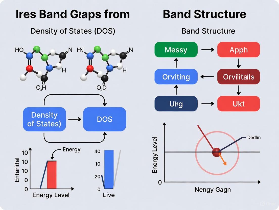
The Density of States (DOS) is a fundamental concept in condensed matter physics and materials science, providing a crucial summary of a material's electronic structure. Unlike a full band structure diagram, which plots electronic energy levels (E) against the wave vector (k), the DOS simplifies this information by focusing solely on energy. It represents the number of available electronic states within a small energy interval at each energy level, effectively acting as a "compressed" version of the band structure [8].
This compression makes DOS an invaluable tool for high-throughput computational screening and rapid property prediction, as it distills complex electronic information into a more manageable form. However, this convenience comes with an inherent trade-off: while DOS retains key information about state density and energy gaps, it necessarily loses the momentum-specific details (k-space information) contained in the full band structure [8]. This article provides a comparative analysis of the accuracy and applications of deriving electronic properties, particularly band gaps, from DOS versus full band structure calculations, examining their respective strengths and limitations within modern materials research.
Fundamental Concepts: DOS vs. Band Structure
Core Definitions and Relationship
The relationship between band structure and DOS is foundational to electronic structure analysis. Band structure diagrams display the allowed electronic energy levels as a function of their crystal momentum (wave vector k), with each point on the band structure curves representing a specific (k, E) state. In contrast, the DOS counts all available states at a given energy level, irrespective of their k-vector, and presents this distribution as a function of energy alone [8].
Key Differences in Information Content:
- Information Retained by DOS: Band gaps, Fermi level position, and density of electronic states at specific energies.
- Information Lost in DOS: k-space specifics, including exact locations of the valence band maximum (VBM) and conduction band minimum (CBM) in the Brillouin zone, band curvatures, and direct versus indirect gap characteristics [8].
This fundamental difference in information content directly impacts the accuracy and suitability of each method for specific applications, particularly in band gap determination.
Visualizing the Relationship
The diagram below illustrates the fundamental relationship between band structure and DOS, showing how the k-dependent information is integrated into an energy-dependent density.
Accuracy Comparison: Band Gaps from DOS vs. Band Structure
Methodological Foundations and Limitations
The accuracy of band gap extraction depends fundamentally on the methodological approach. Band structure analysis allows direct identification of the VBM and CBM within the Brillouin zone, enabling clear distinction between direct and indirect band gaps—a critical determination for optoelectronic applications [8]. However, this approach requires careful calculation of the full electronic band dispersion.
In contrast, DOS-based band gap determination relies on identifying energy regions with zero DOS, indicating band gaps where no electronic states exist. While conceptually simpler, this method faces significant challenges in practice. The primary limitation arises because the DOS approaches zero asymptotically near band edges, making precise identification of the exact gap boundaries difficult, especially in systems with smeared spectral features or computational broadening [9]. This fundamental limitation means DOS-derived band gaps typically exhibit lower accuracy compared to those obtained from direct band structure analysis.
Quantitative Accuracy Assessment
Table 1: Comparative Accuracy of Band Gap Determination Methods
| Method | Computational Cost | Key Strengths | Key Limitations | Typical Band Gap Accuracy |
|---|---|---|---|---|
| DOS Analysis | Low to Moderate | Rapid screening capability; Intuitive interpretation | Cannot distinguish direct/indirect gaps; Asymptotic band edges | Moderate (Highly dependent on system and computational parameters) |
| Full Band Structure | Moderate to High | Direct identification of VBM/CBM; Distinguishes direct/indirect gaps | Computationally intensive; Complex interpretation | High (When using advanced functionals) |
| Hybrid Functionals (e.g., HSE) | High | Corrects band gap underestimation; Improved accuracy | Computationally demanding (~100× GGA cost) [10] | Very High (Close to experimental values) |
| GGA/PBE Functionals | Low | High computational efficiency; Good for structures | Severe band gap underestimation [10] | Low (Systematic underestimation) |
| TB-mBJ Functionals | Moderate | Improved band gaps without Hartree-Fock exchange [11] | Limited availability in codes; Parameter sensitivity | Moderate to High |
The data reveals a clear trade-off between computational efficiency and accuracy. While DOS analysis provides a computationally efficient pathway for band gap estimation, it sacrifices precision and critical diagnostic information about the nature of the gap. Advanced functionals like hybrids or TB-mBJ can significantly improve accuracy but at substantially increased computational cost [10] [11].
Advanced Computational Approaches
Machine Learning for DOS and Band Gap Prediction
Recent advances in machine learning (ML) have created new paradigms for DOS and band gap prediction. PET-MAD-DOS represents a groundbreaking "universal" ML model that predicts DOS directly from atomic configurations using a transformer architecture trained on diverse chemical spaces [9]. This approach demonstrates semi-quantitative agreement with density functional theory (DFT) calculations while being computationally more efficient, enabling high-throughput screening of materials.
Similarly, DOSnet employs convolutional neural networks to automatically extract relevant features from DOS for predicting adsorption energies, demonstrating that ML models can identify complex patterns in DOS that correlate with materials properties [12]. These ML approaches are particularly valuable for finite-temperature molecular dynamics simulations, where they can efficiently compute ensemble-averaged electronic properties across multiple configurations [9].
High-Throughput Databases and Workflows
The emergence of large-scale electronic structure databases has revolutionized materials informatics. The SuperBand database, for instance, provides calculated band structures, DOS, and Fermi surfaces for over 1,362 superconductors, creating standardized datasets for ML training and validation [13]. Such resources enable systematic comparisons between DOS-derived and band structure-derived properties across extensive chemical spaces.
These databases facilitate high-throughput workflows where DOS calculations serve as an efficient initial screening step, followed by more detailed band structure analysis for promising candidates. This hierarchical approach balances computational efficiency with accuracy, leveraging the respective strengths of both methodologies [13].
Experimental Protocols and Methodologies
Standard DFT Workflow for DOS and Band Structure
Table 2: Key Research Reagent Solutions in Computational Materials Science
| Tool/Code | Primary Function | Application Context |
|---|---|---|
| WIEN2k | Full-potential linearized augmented plane wave (FP-LAPW) calculations | Electronic structure calculation of solids [11] |
| VASP | Plane-wave basis set DFT calculations | Surface adsorption and catalytic studies [12] |
| BoltzTraP | Boltzmann transport properties | Calculation of electrical conductivity from band structure [11] |
| OPTIC | Optical property calculations | Dielectric function and reflectivity from electronic structure [11] |
| Hybrid Functionals (HSE) | Mix Hartree-Fock exchange with DFT | Band gap correction and improved accuracy [10] |
| TB-mBJ Potential | Modified Becke-Johnson exchange potential | Improved band gaps without hybrid computational cost [11] |
The experimental workflow for electronic structure analysis typically follows a structured computational pipeline, as visualized below:
Protocol for Accurate Band Offset Calculations
For semiconductor heterojunctions, accurate band alignment requires a specific methodology that combines bulk and interface calculations:
- Bulk Electronic Structure: Perform hybrid functional (HSE) calculations for each bulk material to determine VBM and CBM positions relative to the average electrostatic potential [10].
- Superlattice Construction: Build interface superlattices with sufficient thickness to contain bulk-like regions away from the interface.
- Potential Alignment: Calculate the macroscopic average of the electrostatic potential in the bulk-like regions of each material within the superlattice using GGA, which provides potential alignments within 50 meV of HSE at substantially lower computational cost [10].
- Band Offset Calculation: Combine the potential alignment from the superlattice calculation with the hybrid functional bulk band positions to obtain the final band offsets.
This protocol leverages the accuracy of hybrid functionals for bulk band gaps while utilizing the computational efficiency of GGA for interface potential alignment, achieving an optimal balance between accuracy and computational expense [10].
Case Studies and Applications
Doping Effects in Niobate Catalysts
Research on pristine and doped Nb~3~O~7~(OH) demonstrates the practical application of DOS analysis in catalyst design. DFT calculations reveal that Ta and Sb doping reduces the band gap from 1.7 eV (pristine) to 1.266 eV and 1.203 eV respectively. Partial DOS (PDOS) analysis identifies the orbital origins of this effect: O-p orbitals dominate the valence band while Nb-d orbitals dominate the conduction band in the pristine material, with doping introducing states that reduce the gap [11].
This DOS-based analysis successfully explains the red-shift in optical absorption to the visible region, enabling enhanced photocatalytic activity. However, the distinction between direct and indirect band gaps—critical for assessing photocatalytic efficiency—required complementary band structure calculations, which confirmed direct gap behavior in both pristine and doped systems [11].
Machine Learning for Adsorption Energy Prediction
The DOSnet framework demonstrates how ML can extract features from DOS that correlate with catalytic properties. By using convolutional neural networks to automatically process DOS data, this approach achieves mean absolute errors of approximately 0.1 eV for predicting adsorption energies across diverse surfaces and adsorbates [12].
This application highlights a key advantage of DOS over full band structure for high-throughput screening: the simplified, lower-dimensional nature of DOS data enables more efficient feature extraction by ML algorithms, facilitating rapid prediction of materials properties without explicit identification of band structure characteristics [12].
The choice between DOS analysis and full band structure calculations represents a fundamental trade-off between computational efficiency and informational completeness. DOS provides a compressed, efficient representation suitable for high-throughput screening, rapid conductivity assessment, and initial band gap estimation. Its strength lies in identifying state distributions and general electronic trends without k-space complexity.
Full band structure analysis remains essential for precise band gap determination, distinguishing direct and indirect gaps, calculating carrier effective masses, and understanding detailed electronic transitions. While computationally more demanding, it provides unambiguous identification of critical band extrema and their locations in the Brillouin zone.
For modern materials research, the most effective strategies employ hierarchical approaches: using DOS for rapid screening of large materials spaces, followed by targeted band structure calculations for promising candidates. The integration of machine learning with both methodologies further enhances this paradigm, enabling increasingly accurate predictions while managing computational costs. As database resources expand and algorithms improve, this synergistic combination will continue to drive advancements in electronic structure prediction and materials design.
The electronic band structure of a material, which describes the allowed energy levels of electrons as a function of their momentum in k-space, serves as a foundational concept in condensed matter physics and materials science. It provides critical insights into a material's electronic, optical, and transport properties, enabling researchers to design novel materials for applications ranging from semiconductors to catalysis and drug development. The accurate prediction of band gaps—the energy difference between the valence band maximum (VBM) and conduction band minimum (CBM)—remains a central challenge, as this parameter fundamentally governs a material's behavior in electronic and optoelectronic devices.
Two primary computational approaches have emerged for determining electronic properties: direct band structure calculation and indirect estimation from the density of states (DOS). Direct band structure methods solve the Kohn-Sham equations along high-symmetry paths in the Brillouin zone, providing a detailed momentum-resolved energy map. In contrast, DOS-based approaches compute the distribution of electronic states across energy levels, from which band gaps can be inferred by identifying energy ranges with zero DOS. While both methods aim to characterize electronic structure, they differ significantly in computational cost, information completeness, and practical accuracy—considerations crucial for researchers selecting appropriate methodologies for material screening and property prediction.
Table: Fundamental Approaches to Electronic Structure Calculation
| Method Type | Key Output | Band Gap Determination | Momentum Resolution |
|---|---|---|---|
| Band Structure | Energy vs. k-point dispersion | Direct from VBM and CBM positions | Full k-dependent information |
| Density of States (DOS) | States per unit energy | Identified from DOS valleys | No k-resolution |
Theoretical Frameworks and Computational Methods
First-Principles Electronic Structure Methods
First-principles computational methods form the backbone of modern electronic structure prediction, with Density Functional Theory (DFT) serving as the workhorse for high-throughput screening. Standard DFT functionals, particularly those within the generalized gradient approximation (GGA), systematically underestimate band gaps due to self-interaction errors, prompting the development of more advanced corrections. The Hubbard U correction (DFT+U) addresses electron localization in strongly correlated systems like metal oxides by applying an onsite Coulomb interaction. Recent studies demonstrate that applying U corrections to both metal d/f orbitals and oxygen p orbitals significantly improves accuracy for oxides like TiO₂, ZnO, and CeO₂, with optimal (Uₚ, U_d/f) pairs yielding band gaps within 0.1-0.2 eV of experimental values [14].
Beyond DFT+U, hybrid functionals like HSE06 incorporate a portion of exact Hartree-Fock exchange, improving band gap predictions at increased computational cost. The TB-mBJ functional has emerged as a promising meta-GGA approach, providing improved band gaps without the computational expense of hybrids, as demonstrated in studies of Nb₃O₇(OH) where it accurately captured band gap reductions from 1.7 eV (pristine) to 1.266 eV (Ta-doped) and 1.203 eV (Sb-doped) systems [11].
For highest accuracy, many-body perturbation theory within the GW approximation has become the gold standard, systematically improving upon DFT by directly computing electron self-energies. Different GW flavors offer varying balances of accuracy and computational expense: (1) G₀W₀ using plasmon-pole approximation (PPA) provides marginal improvements over DFT hybrids; (2) full-frequency quasiparticle G₀W₀ dramatically improves predictions; (3) quasiparticle self-consistent GW (QSGW) removes starting-point dependence but overestimates gaps by ~15%; and (4) QSGŴ with vertex corrections achieves exceptional accuracy, reliably flagging questionable experimental measurements [6].
Table: Accuracy Comparison of Electronic Structure Methods
| Method | Theoretical Foundation | Typical Band Gap Error | Computational Cost | Key Applications |
|---|---|---|---|---|
| GGA/PBE | DFT | Severe underestimation (30-50%) | Low | High-throughput screening |
| HSE06 | Hybrid DFT | Underestimation (10-20%) | High | Moderate-scale accurate calculations |
| TB-mBJ | Meta-GGA DFT | Moderate error (5-15%) | Medium | Optoelectronic materials |
| G₀W₀@GGA | Many-body perturbation theory | Variable, depends on starting point | High | Small systems validation |
| QSGŴ | GW with vertex corrections | Highest accuracy (<5%) | Very High | Benchmark calculations |
Machine Learning Approaches
The rising computational cost of high-accuracy methods has spurred development of machine learning (ML) models that predict electronic properties directly from atomic structures. These approaches include specialized models targeting specific properties and universal models applicable across diverse chemical spaces.
DOS-based ML methods represent one prominent approach. The PET-MAD-DOS model uses a rotationally unconstrained transformer architecture trained on the Massive Atomistic Diversity dataset to predict DOS, from which band gaps can be derived by identifying the Fermi level and locating the VBM and CBM [9]. While this approach achieves semiquantitative agreement, challenges remain in precisely determining band edges from predicted DOS, particularly for systems with small or zero band gaps.
End-to-end band structure prediction represents a more direct approach. The Bandformer model employs a graph transformer architecture that treats crystal structures as input "sentences" and translates them to band energy sequences as output [15]. This method uses Fast Fourier Transform to capture oscillatory patterns in band dispersions and achieves a mean absolute error of 0.251 eV for band gap prediction on a diverse dataset of 27,772 materials from the Materials Project database.
Hybrid DFT-ML approaches combine physical simulations with data-driven modeling. For metal oxides, ML models can learn the relationship between Hubbard U parameters and resulting band gaps, enabling accurate predictions at a fraction of the computational cost of full DFT+U calculations [14]. Similarly, DOSnet uses convolutional neural networks to automatically extract relevant features from DOS for predicting adsorption energies, demonstrating the utility of learned electronic descriptors for materials properties [12].
Methodological Comparisons and Experimental Validation
Accuracy Benchmarking Across Methods
Recent systematic benchmarking provides crucial insights into the relative performance of electronic structure methods. A comprehensive assessment of GW methods against top-performing DFT functionals (mBJ and HSE06) across 472 non-magnetic materials revealed that G₀W₀ with plasmon-pole approximation offers only marginal improvements over the best DFT methods despite higher computational cost [6]. However, replacing PPA with full-frequency integration dramatically improved predictions, nearly matching the accuracy of QSGŴ with vertex corrections. The most accurate method, QSGŴ, essentially eliminated systematic errors, producing band gaps sufficiently reliable to identify questionable experimental measurements.
For specific material classes, method performance varies significantly. In metal oxides, DFT+U with carefully chosen (Uₚ, U_d/f) parameters achieves accuracy competitive with more expensive methods, with optimal pairs including (8 eV, 8 eV) for rutile TiO₂; (3 eV, 6 eV) for anatase TiO₂; and (7 eV, 12 eV) for c-CeO₂ [14]. The TB-mBJ functional has demonstrated strong performance for complex materials like Nb₃O₇(OH), correctly capturing band gap engineering through doping and providing accurate optical property predictions [11].
ML methods show promising but variable accuracy. The Bandformer model achieves approximately 0.25 eV MAE for band gaps [15], while DOS-derived band gaps from PET-MAD-DOS show larger errors, particularly for challenging systems like clusters with sharply-peaked DOS [9]. This accuracy gap between direct band structure prediction and DOS-derived approaches highlights the fundamental information loss when collapsing momentum-resolved data into energy distributions.
Experimental Validation Protocols
Rigorous experimental validation remains essential for assessing computational predictions. Multiple techniques provide complementary approaches for band structure characterization:
Direct experimental band structure mapping using angle-resolved photoemission spectroscopy (ARPES) provides the most comprehensive validation, directly measuring energy-momentum dispersion relations. For instance, studies on LiGaSe₂ compared DFT calculations using GGA and HSE06 functionals (predicting 2.02 eV and 2.75 eV gaps, respectively) against experimental absorption spectra indicating a 1.71 eV gap [16], highlighting the systematic overestimation of hybrid functionals for this material.
Indirect optical measurements including absorption spectroscopy and diffuse reflectance provide experimental band gaps by identifying the fundamental absorption edge. For CrB₂, combined aberration-corrected TEM with electron energy loss spectroscopy validated the AlB₂-type structure and chemical bonding patterns predicted by DFT [17], demonstrating how multiple experimental techniques can collectively validate computational predictions.
Transport measurements offer additional validation by probing band structure through electrical properties like effective mass and carrier mobility. For Nb₃O₇(OH), calculated transport properties including electrical conductivity provided additional validation of the predicted electronic structure [11].
The diagram below illustrates the workflow for computational band structure prediction and experimental validation:
Research Reagent Solutions: Computational Tools for Band Structure Analysis
Table: Essential Computational Tools for Band Structure Research
| Tool Name | Type | Key Functionality | Methodology |
|---|---|---|---|
| Quantum ESPRESSO [6] [16] | Plane-wave DFT Code | Electronic structure, phonons, MD | DFT, DFPT using plane-wave basis sets |
| VASP [14] [16] | Plane-wave DFT Code | Electronic structure, optimization | DFT, hybrid DFT, GW using PAW method |
| BerkeleyGW [18] | Many-Body Perturbation Code | Quasiparticle energies, screening | GW/BSE with plane-wave basis |
| WIEN2k [11] | All-Electron DFT Code | Electronic structure, optics, transport | FP-LAPW method with all-electron treatment |
| CRYSTAL [16] | LCAO Code | Electronic structure, properties | LCAO with Gaussian-type orbitals |
| Bandformer [15] | ML Model | End-to-end band structure prediction | Graph transformer architecture |
| PET-MAD-DOS [9] | ML Model | Density of states prediction | Point Edge Transformer architecture |
The comprehensive comparison of band structure methodologies reveals a complex accuracy-cost tradeoff landscape. While direct band structure calculations using advanced GW methods (particularly QSGŴ) currently provide the highest accuracy, their computational expense limits application to small systems. In contrast, DOS-based approaches offer computational efficiency but sacrifice momentum resolution and introduce uncertainties in band gap determination, particularly for systems with complex band edge character.
For high-throughput screening, machine learning models show tremendous promise, with end-to-end band structure prediction outperforming DOS-derived gaps in accuracy. However, ML models remain limited by their training data quality and diversity, struggling with extrapolation to novel material classes. The emerging paradigm of hybrid physics-ML approaches, combining the interpretability of physical models with the efficiency of data-driven methods, offers a promising path forward.
As computational resources grow and algorithms advance, the integration of multi-fidelity datasets combining low-cost calculations with high-accuracy benchmarks will enable more robust predictive models. For researchers navigating this complex landscape, method selection should be guided by target material class, desired property predictions, and available computational resources, with experimental validation remaining essential for confirming computational insights.
In the field of condensed matter physics and computational materials science, understanding the electronic structure of a material is fundamental to predicting its properties. Two of the most common tools for this analysis are the Band Structure and the Density of States (DOS). While both are derived from the same underlying quantum mechanical foundations and are intrinsically related, they provide different perspectives and retain different types of information. The choice between them can significantly impact the accuracy and efficiency of research, particularly in critical applications like semiconductor design and drug development where precise band gap information is crucial. This guide provides a detailed, objective comparison of these two methods, focusing on their respective strengths and limitations to inform researchers and scientists in their selection process.
Fundamental Concepts: Band Structure vs. Density of States
Band Structure: The Momentum-Resolved Picture
The electronic band structure is a representation of the allowed energy levels (eigenvalues) for electrons in a periodic crystal, plotted as a function of their crystal momentum vector k in the Brillouin zone. Essentially, it shows the energy E of an electron as a function of its wave vector k (which relates to its momentum). Each line on a band structure plot represents a specific electronic band, revealing how the energy of electrons changes with their direction and wavelength of propagation within the crystal. Band structure diagrams are essential for understanding direction-dependent electronic properties, such as effective mass and carrier velocity [8].
Density of States: The Energy-Resolved Picture
The Density of States (DOS) describes the number of available electron states per unit volume per unit energy interval. In simpler terms, it counts how many electronic states are "packed" at each energy level, effectively integrating over all possible momentum (k-space) values. It is defined as ( D(E) = \frac{1}{V} \frac{\mathrm{d}N(E)}{\mathrm{d}E} ), where ( N(E) ) is the number of states up to energy ( E ), and ( V ) is the volume [19] [20]. The DOS acts as a "compressed" version of the band structure, preserving information about the distribution of states in energy but discarding the momentum information [8].
Table: Core Conceptual Differences Between Band Structure and Density of States
| Feature | Band Structure | Density of States (DOS) |
|---|---|---|
| Primary Variables | Energy (E) vs. Momentum (k) | Density of States (D) vs. Energy (E) |
| Dimensionality | Multidimensional (e.g., E(kx, ky, kz)) | One-dimensional (D(E)) |
| Information Focus | Direction-dependent electronic properties | Total available states at a given energy |
| Visual Representation | Dispersive bands plotted along high-symmetry paths in the Brillouin zone | A curve, often with peaks (van Hove singularities) where bands are flat |
Information Retained and Omitted: A Detailed Comparison
Information Retained by Density of States
The DOS is exceptionally efficient at capturing and presenting several key pieces of information:
- Band Gap Presence and Size: The DOS is a direct indicator of whether a material is a metal, semiconductor, or insulator. A zero DOS at the Fermi level (EF) signifies a band gap, and the energy range where DOS is zero corresponds to the band gap size [19] [8].
- Total State Availability: It quantifies the number of electronic states available at any given energy, which is crucial for calculating properties like the specific heat and paramagnetic susceptibility of conductive solids [20].
- Orbital Contributions (via PDOS): Through Projected DOS (PDOS), the total DOS can be decomposed into contributions from specific atoms, atomic orbitals (s, p, d, f), or molecular fragments. This is invaluable for understanding bonding, the role of dopants, and catalytic activity [8].
Information Omitted by Density of States
The process of integrating over momentum space to create the DOS comes at the cost of losing specific, momentum-resolved information:
- k-Space Location: The DOS does not reveal where in the Brillouin zone a state exists. It loses all information about the electron's momentum [8].
- Direct vs. Indirect Band Gap: This is a critical omission. The DOS can confirm a band gap exists and measure its size, but it cannot determine if the gap is direct (the maximum of the valence band and the minimum of the conduction band occur at the same k-point) or indirect (they occur at different k-points). This distinction is vital for optoelectronic applications [8].
- Band Dispersion and Effective Mass: The curvature of bands in the band structure diagram determines the effective mass of electrons and holes, which governs carrier mobility. The DOS, being energy-focused, cannot provide this information [8].
Table: Information Retention in DOS vs. Band Structure
| Information Type | Retained in DOS? | Retained in Band Structure? |
|---|---|---|
| Band gap existence | Yes | Yes |
| Band gap size (energy) | Yes | Yes |
| Direct vs. indirect nature of band gap | No | Yes |
| Fermi level position | Yes | Yes |
| Orbital character (via projection) | Yes (PDOS) | Possible, but more complex |
| Carrier effective mass | No | Yes (from band curvature) |
| Momentum (k) of electronic states | No | Yes |
| Anisotropy of electronic properties | No | Yes |
Diagram: Information Flow and Retention in Band Structure vs. Density of States
Experimental and Computational Protocols
Methodologies for Band Gap Extraction
The protocols for determining band gaps from DOS and band structure differ significantly, leading to potential variations in accuracy and interpretation.
From Band Structure: The methodology involves identifying the valence band maximum (VBM) and the conduction band minimum (CBM) across the entire Brillouin zone. The fundamental band gap is calculated as Egap = ECBM - EVBM. To classify the gap as direct or indirect, the k-points of the VBM and CBM are compared. If they are identical, the gap is direct; if not, it is indirect [21]. This method is considered the ground truth for determining the nature of the band gap.
From Density of States: The band gap is identified by locating the energy region between the valence band and the conduction band where the DOS value is zero. The size of the gap is the energy width of this zero-DOS region. However, this method inherently cannot provide information on whether the VBM and CBM are co-located in k-space, thus failing to distinguish between direct and indirect gaps [8].
Quantitative Accuracy Comparison in Research
Comparative studies highlight the practical implications of choosing one method over the other. Research involving materials like InAs, GaAs, and InGaAs has shown that band structures computed with advanced models (e.g., density functional theory, tight-binding) are necessary for accurately simulating device performance, such as the drain current in nanoscale MOSFETs. Relying solely on DOS-derived parameters can lead to inaccuracies because the DOS omits the critical k-space information that affects carrier transport [22].
Furthermore, modern machine learning approaches are being developed to bridge the gap between experimental data and band structure reconstruction. These pipelines can reconstruct complex band dispersions, such as all 14 valence bands of tungsten diselenide (WSe2), uncovering momentum-space structural information that is inaccessible from DOS analysis alone [21]. This underscores the limitation of DOS for detailed electronic structure benchmarking.
Table: Experimental Data Comparison for Band Gap Accuracy
| Material | Calculation Method | Band Gap from Band Structure (eV) | Band Gap from DOS (eV) | Key Finding / Discrepancy |
|---|---|---|---|---|
| InGaAs Quantum Wells | Density Functional Theory (DFT) & Effective Mass Models | Accurately captures thickness-dependent gap variation [22] | Yields same energy gap but misses k-space location [22] | DOS-derived gaps insufficient for predicting ballistic current in MOSFETs; full band structure needed for transport simulation [22]. |
| WSe2 | Machine Learning Reconstruction of ARPES data | Reconstructs 14 valence bands with momentum resolution < 0.02 Å⁻¹ [21] | Not the primary method for detailed assessment [21] | Band structure enables global quantitative benchmarking against theory; DOS alone would lose the momentum-resolution required [21]. |
| General Semiconductors | Various | Distinguishes direct vs. indirect gaps | Cannot distinguish direct vs. indirect gaps | This fundamental omission by DOS can lead to incorrect material selection for applications like lasers (require direct gap) [8]. |
The Scientist's Toolkit: Key Reagents and Computational Solutions
For researchers embarking on electronic structure analysis, the following tools and concepts are essential.
Table: Essential Research Reagent Solutions for Electronic Structure Analysis
| Research Reagent / Tool | Function / Explanation |
|---|---|
| Density Functional Theory (DFT) | A computational quantum mechanical method used to model the electronic structure of many-body systems. It is the workhorse for calculating both band structures and DOS. |
| Angle-Resolved Photoemission Spectroscopy (ARPES) | An experimental technique that directly measures the band structure of materials by probing the energy and momentum of photoemitted electrons [21]. |
| Projected Density of States (PDOS) | A computational analysis that decomposes the total DOS into contributions from specific atomic orbitals, essential for understanding bonding and dopant effects [8]. |
| Markov Random Field (MRF) Models | A probabilistic machine learning framework used to reconstruct band structures from experimental photoemission data, improving scalability and accuracy over traditional fitting methods [21]. |
| d-band Center Analysis | A parameter derived from the PDOS of transition metals' d-orbitals; its position relative to the Fermi level is a powerful descriptor for predicting catalytic activity [8]. |
The choice between Density of States and Band Structure is not a matter of one being universally superior to the other, but rather of selecting the right tool for the specific research question.
- Use Density of States (DOS) when: Your goal is a quick assessment of whether a material is metallic or insulating, to determine the fundamental band gap size (but not its nature), to calculate total quantities like specific heat, or to analyze orbital contributions via PDOS for understanding bonding or catalytic sites. It is more concise and often easier for non-experts to interpret for these specific purposes [8].
- Use Band Structure when: The precise nature of the band gap (direct vs. indirect) is critical, as in optoelectronic device design. It is also essential for understanding direction-dependent properties (anisotropy), calculating carrier effective mass and mobility, and for any detailed comparison with momentum-resolved experimental techniques like ARPES [22] [8] [21].
For a comprehensive understanding, the most robust strategy is to use both tools in concert. The DOS provides a quick overview and analysis of state distributions, while the band structure supplies the essential, omitted details on momentum space needed for accurate predictions of material behavior in devices and complex applications.
In the field of computational materials science, researchers frequently face decisions about the most efficient computational methods for electronic structure analysis. Density of States (DOS) and full band structure calculations represent two complementary approaches with distinct trade-offs in computational cost, information content, and practical application. Within the context of a broader thesis on accuracy comparison for band gaps, this guide objectively examines scenarios where a rapid DOS analysis provides sufficient insight while conserving computational resources. DOS serves as a "compressed" version of band structure, preserving key information like band gaps and state distributions while omitting momentum-specific details [8]. Understanding when to prioritize efficiency over comprehensive analysis enables researchers to optimize their computational workflows, particularly in high-throughput materials screening and initial characterization studies.
Key Concepts: DOS vs. Band Structure
Fundamental Differences
The electronic band structure of a material plots allowed electron energy levels (E) against the wave vector (k), which relates to electron momentum in a crystalline solid [8]. This provides a complete picture of electronic dispersion relationships across different crystal momentum directions. In contrast, the Density of States (DOS) simplifies this information by counting the number of available electronic states within specific energy intervals, effectively "compressing" the band structure into an energy-dependent density plot [8].
Projected Density of States (PDOS) extends this concept by decomposing contributions from specific atoms or orbitals (s, p, d, f), revealing atomic-level contributions to electronic properties [8]. This decomposition is particularly valuable for understanding doping effects, bonding character, and catalytic mechanisms in complex materials.
Information Content Comparison
Table: Information Content in DOS vs. Band Structure Calculations
| Aspect | Band Structure | Density of States (DOS) |
|---|---|---|
| Primary Information | Energy levels vs. wave vector (k) in specific crystallographic directions | Number of electronic states per energy interval |
| Band Gap Determination | Direct and indirect gaps distinguishable via k-space analysis | Total gap measurable, but indirect/direct nature ambiguous |
| k-Space Resolution | Complete momentum-resolved electronic dispersion | Momentum-averaged, no directional information |
| Computational Demand | Higher (requires calculation along specific k-point paths) | Lower (requires calculation at representative k-points) |
| Typical Applications | Carrier effective mass analysis, optical transition studies | Quick conductivity assessment, orbital contribution analysis, doping effects |
When to Prefer DOS Analysis: Practical Scenarios
High-Throughput Material Screening
In high-throughput computational screening for materials design and discovery, DOS analysis provides a rapid method for assessing fundamental electronic properties across numerous candidate structures. The compressed nature of DOS enables quick identification of metals (non-zero DOS at Fermi level) versus insulators/semiconductors (zero DOS at Fermi level) without the computational overhead of full band structure calculations [8]. This approach is particularly valuable in initial screening stages for photovoltaic applications, where researchers must quickly eliminate candidates with inappropriate band gap characteristics from larger material databases.
Experimental Protocol: For high-throughput DOS screening, researchers typically employ density functional theory (DFT) calculations with a representative k-point mesh (e.g., Monkhorst-Pack scheme) [23]. The workflow involves: (1) structural optimization of candidate materials, (2) self-consistent field calculations with appropriate k-point sampling, (3) DOS calculation with projected components, and (4) automated analysis of results focusing on Fermi level position and band gap estimation.
Initial Assessment of Doping Effects
DOS and particularly PDOS excel in initial investigations of doping effects on electronic structure. When introducing dopants into host materials, PDOS quickly reveals the formation of new electronic states within band gaps and identifies the orbital origins of these states [8]. For example, nitrogen doping in TiO₂ creates occupied N-2p states above the O-2p valence band, effectively narrowing the band gap for enhanced visible-light absorption [8]. This information is obtainable without computationally expensive band structure calculations along high-symmetry directions.
Experimental Protocol: Analyzing doping effects via PDOS involves: (1) constructing supercell models with appropriate dopant concentrations, (2) performing geometric optimization while constraining dopant positions, (3) calculating PDOS with projections onto dopant and neighboring atoms, and (4) comparing with undoped system PDOS to identify dopant-induced states. The k-point sampling can often be sparser than required for accurate band structure calculations.
Bonding Analysis and Orbital Interactions
For understanding chemical bonding and orbital interactions in crystalline materials, PDOS provides more direct insight than full band structures. When adjacent atoms show significant PDOS overlaps at specific energies, this indicates bonding interactions between their orbitals [8]. This approach is invaluable in catalyst design, where adsorption strengths correlate with specific orbital overlaps between surface atoms and adsorbates [8]. The Crystal Orbital Overlap Population (COOP) analysis extends this concept by quantifying bonding character across energy ranges [24].
Diagram: PDOS Bonding Analysis Workflow. COOP analysis quantifies bonding/antibonding interactions between atomic orbitals.
Rapid Characterization of Conductivity Properties
DOS provides sufficient information for initial conductivity type assessment in materials research. The presence or absence of states at the Fermi level immediately distinguishes metallic from insulating/semiconducting behavior [8]. While DOS cannot determine effective masses or mobility directly, it quickly identifies potential conductors versus insulators, which is particularly valuable when sorting through novel material systems where basic transport properties are unknown.
Resource-Constrained Computational Environments
In computational resource-limited scenarios, DOS analysis offers a practical compromise between information content and calculation cost. Full band structure calculations require electronic structure evaluation along dense k-point paths through the Brillouin zone, while DOS calculations can use sparser k-point meshes while still capturing essential state distribution information [8] [23]. This efficiency difference becomes particularly significant for large supercells, complex unit cells, or when using computationally expensive methods like hybrid DFT.
Experimental Data and Accuracy Comparison
Band Gap Determination: DOS vs. Band Structure
Table: Band Gap Accuracy Comparison Between Methods
| Material System | Calculation Method | DOS-Derived Band Gap (eV) | Band Structure-Derived Band Gap (eV) | Experimental Reference (eV) | Key Observations |
|---|---|---|---|---|---|
| CsPbBr₃ Perovskite (Non-relativistic) | GGA-PBEsol [24] | Metallic (no gap) | Metallic (no gap) | ~2.3 [24] | Both methods correctly identify metallic nature without relativistic treatment |
| CsPbBr₃ Perovskite (Scalar Relativistic) | GGA-PBEsol [24] | ~1.2 eV | ~1.2 eV | ~2.3 [24] | Both methods show gap opening but underestimate experimental value |
| TiO₂ (Anatase) | DFTB [23] | ~2.1 eV (from DOS plot) | Not specified | ~3.2 eV | DOS clearly shows gap but functional-dependent underestimation |
| HgBa₂CuO₄ | First-principles [25] | Small DOS at E_F | pdσ* band crosses E_F | Metallic | Both methods correctly identify metallic behavior |
Computational Efficiency Metrics
The computational advantage of DOS analysis manifests in several quantitative metrics:
k-Point Requirements: DOS calculations typically require only a representative k-point mesh (e.g., 4×4×4 Monkhorst-Pack for anatase TiO₂ [23]), while band structure calculations need additional computations along specific high-symmetry paths with fine resolution (e.g., 20 points between Γ and X [23]).
Timing Comparisons: For the CsPbBr₃ perovskite system [24], DOS/PDOS calculations added minimal overhead to the base self-consistent field calculation, while full band structure computation along the Γ-X-M-R-Γ path required approximately 30-50% additional computational time depending on path point density.
Research Reagent Solutions: Computational Tools
Table: Essential Computational Tools for Electronic Structure Analysis
| Tool/Software | Primary Function | Key Features | Application Context |
|---|---|---|---|
| VASP [26] | DFT Calculator | DOS, band structure, PDOS capabilities | Full first-principles calculations with plane-wave basis sets |
| DFTB+ [23] | DFTB Calculator | Efficient DOS/band structure with tight-binding | Large systems, rapid screening, parameterized methods |
| AMS BAND [24] | DFT Package | DOS, PDOS, COOP analysis | Chemical bonding analysis in periodic systems |
| dp_dos [23] | Analysis Tool | DOS processing and visualization | Post-processing of DFTB+ results for plotting |
| SCM-ADF [27] | DOS Analysis | TDOS, GPDOS, OPDOS, PDOS | Mulliken population-based DOS analysis |
The choice between DOS analysis and full band structure calculations represents a fundamental trade-off between computational efficiency and information completeness. DOS analysis proves superior in practical scenarios including high-throughput material screening, initial doping effect assessment, bonding character analysis, rapid conductivity typing, and resource-constrained environments. The compressed nature of DOS information provides sufficient data for many materials design decisions while conserving computational resources.
For band gap characterization specifically, DOS provides accurate identification of insulating versus metallic behavior and reasonable band gap estimates, though it cannot distinguish between direct and indirect gaps—a significant limitation for optoelectronic applications. Researchers should consider DOS analysis as an efficient first pass in hierarchical computational workflows, reserving more expensive band structure calculations for promising candidates requiring detailed electronic dispersion analysis. This balanced approach maximizes research productivity while maintaining scientific rigor in electronic structure analysis.
From Theory to Practice: Implementing DOS and Band Structure Analysis
A Step-by-Step Workflow for Band Gap Calculation from DOS
In computational materials science, the accurate prediction of electronic band gaps is paramount for understanding and designing semiconductors, catalysts, and optoelectronic devices. While several computational methods exist for band gap determination, analysis of the Density of States (DOS) provides a particularly accessible approach. The DOS represents the number of available electronic states per unit volume per unit energy, effectively serving as a "compressed" version of the band structure that focuses solely on energy distribution rather than momentum space details [8]. This simplification makes DOS analysis invaluable for rapid assessments of electronic properties, though it comes with specific limitations regarding accuracy and information completeness.
The broader thesis context of accuracy comparison between DOS-derived and band structure-derived band gaps reveals a complex landscape where methodological choices significantly impact results. This guide provides an objective, step-by-step workflow for calculating band gaps from DOS, compares its performance against alternative methods, and presents supporting experimental data to guide researchers in selecting appropriate protocols for their specific applications, particularly in materials design and drug development research where semiconductor properties influence device performance and sensing capabilities.
Theoretical Foundation: DOS vs. Band Structure
Fundamental Concepts and Relationships
The electronic band structure of a material describes the energy levels of electrons as a function of their crystal momentum (wave vector k) in the reciprocal space. In contrast, the Density of States (DOS) simplifies this complex relationship by counting all available electronic states at each energy level, regardless of their k-vector [8]. Mathematically, the DOS is defined as the number of electronic states in the energy interval ρ(E)dE\rho(E)dE, and is obtained by integrating the band structure over the Brillouin zone [8] [28].(E,E+dE)(E,E+dE)
Key Differences Between DOS and Band Structure:
- Information Retained: Both methods preserve fundamental band gaps and Fermi level positions [8]
- Information Lost: DOS analysis omits k-space specifics, including direct vs. indirect gap distinctions and band curvature details that determine carrier effective masses [8]
- Practical Considerations: DOS provides a more concise representation for property prediction, while band structure contains complete electronic dispersion information [8]
The peaks in DOS correspond to van Hove singularities—energy regions where the electronic bands exhibit flat dispersion, resulting in a high concentration of states [28]. These features make DOS particularly useful for identifying energy regions with high state availability for electronic transitions and chemical bonding.
When DOS Analysis Is Preferred
DOS analysis provides distinct advantages in several research scenarios:
- High-Throughput Screening: Rapid characterization of conductivity (metallic vs. insulating behavior) across multiple material systems [8]
- Orbital Contribution Analysis: Projected DOS (PDOS) decomposes contributions by specific atoms or orbitals (s, p, d, f), revealing atomic-level contributions to electronic properties [8]
- Bonding Analysis: PDOS overlaps between adjacent atoms indicate chemical bonding interactions [8]
- Catalysis Research: d-band center theory utilizes PDOS of transition metals to predict catalytic activity [8]
Computational Workflows: A Step-by-Step Guide
Density Functional Theory Workflow for DOS Calculation
The following workflow outlines the standard procedure for calculating DOS using plane-wave DFT codes such as Quantum ESPRESSO:
Figure 1: DFT Workflow for DOS Calculation. This standardized protocol ensures reproducible DOS calculations across different material systems.
Step 1: Structure Preparation Begin with a fully relaxed crystal structure to ensure accurate lattice parameters. Using experimental lattice constants without relaxation may introduce artificial stress that affects electronic properties [29].
Step 2: Self-Consistent Field (SCF) Calculation Perform a fixed-ion SCF calculation to obtain the converged ground-state charge density. Key parameters include:
- ecutwfc: Plane-wave cutoff energy (increase for better precision)
- k-point grid: Moderate grid (e.g., 4×4×4) for initial convergence
- pseudopotential: Appropriate norm-conserving or ultrasoft pseudopotentials [29]
Step 3: Non-Self Consistent Field (NSCF) Calculation Using the converged charge density from SCF, perform an NSCF calculation with a denser k-point grid:
- k-point grid: Denser grid (e.g., 12×12×12) for accurate Brillouin zone integration
- occupations: Set to 'tetrahedra' for DOS calculations
- nosym: Set to .TRUE. to prevent k-point symmetry operations in low-symmetry cases
- nbnd: Include additional unoccupied bands to ensure complete DOS spectrum [29]
Step 4: DOS Calculation Execute the DOS calculation using the NSCF output:
- prefix: Must match SCF and NSCF calculations
- outdir: Consistent directory across all steps
- emin/emax: Set appropriate energy range around Fermi level
- fildos: Specify output DOS filename [29]
Step 5: Band Gap Extraction From the calculated DOS, identify the band gap as the energy region between the valence band maximum (VBM) and conduction band minimum (CBM) where DOS approaches zero. The Fermi energy typically separates occupied and unoccupied states [8].
Advanced Many-Body Perturbation Theory Workflow
For higher accuracy, particularly in systems with strong electronic correlations, many-body perturbation theory (GW approximation) provides a more rigorous framework:
Figure 2: GW Methodology Hierarchy. Increasing computational cost and accuracy from left to right, with vertex corrections providing the most physically rigorous treatment.
The GW approach corrects the systematic band gap underestimation of standard DFT by approximating the electron self-energy. Key variants include [6]:
- G₀W₀-PPA: One-shot GW using plasmon-pole approximation (PPA); marginally more accurate than best DFT functionals but at higher computational cost
- QP G₀W₀: Full-frequency quasiparticle GW without PPA; significantly improves accuracy over G₀W₀-PPA
- QSGW: Quasiparticle self-consistent GW; removes starting-point dependence but systematically overestimates experimental gaps by ~15%
- QSGŴ: QSGW with vertex corrections in screened Coulomb interaction; provides highest accuracy, reliably identifying questionable experimental measurements [6]
Accuracy Comparison: Methodological Benchmarking
Quantitative Performance Assessment
Table 1: Band Gap Accuracy Comparison Across Computational Methods
| Method | Mean Absolute Error (eV) | Systematic Bias | Computational Cost | Typical Use Case |
|---|---|---|---|---|
| LDA/PBE DFT | 1.0-2.0 [6] | Severe underestimation | Low | High-throughput screening |
| HSE06 Hybrid DFT | 0.3-0.5 [6] | Moderate underestimation | Medium | Standard accuracy studies |
| mBJ Meta-GGA | 0.3-0.6 [6] | Variable | Low-medium | Solid-state spectroscopy |
| G₀W₀-PPA | 0.2-0.4 [6] | Slight underestimation | High | Moderate accuracy correction |
| QP G₀W₀ | 0.15-0.3 [6] | Minimal systematic error | Very high | Accurate property prediction |
| QSGW | 0.2-0.3 [6] | ~15% overestimation | Very high | Fundamental studies |
| QSGŴ | 0.1-0.2 [6] | Minimal systematic error | Extreme | Benchmark-quality results |
The performance data reveals that while advanced DFT functionals like HSE06 and mBJ offer significant improvements over semilocal DFT at moderate computational cost, GW methods generally provide superior accuracy, particularly when including full-frequency integration and vertex corrections [6].
Band gaps extracted from DOS calculations face several specific challenges:
k-point Sampling: Sparse k-point grids can artificially open band gaps by missing the actual VBM/CBM locations [4]. For example, using even-numbered k-grids might exclude the Γ-point where critical band extrema often occur [29].
Smearing Effects: Gaussian or tetrahedron smearing methods can artificially fill the band gap region with non-zero DOS, leading to underestimation of the true gap [29].
Projection Errors: In PDOS analysis, the sum of orbital projections may slightly undercount the total DOS, potentially affecting gap identification [8].
Methodological Consistency: Differences between DOS and band structure gaps often stem from using different k-point sets for the two calculations [4].
Experimental Protocols and Validation
Experimental Benchmarking Procedures
Validating computational band gap predictions requires careful experimental comparison:
Optical Spectroscopy Validation
- UV-Vis Spectroscopy: Measure absorption coefficient and extract Tauc plot for direct/indirect gap determination
- Ellipsometry: Determine dielectric function and critical point energies
- Photoluminescence Excitation: Identify fundamental gap through emission thresholds
Photoemission Spectroscopy
- XPS/UPS: Directly measure occupied valence band states and work function
- Inverse Photoemission: Probe unoccupied conduction band states
- ARPES: Map band dispersion with high angular resolution
Electrical Characterization
- Temperature-Dependent Conductivity: Activate carriers across band gap
- Hall Effect Measurements: Determine carrier concentration and type
Machine Learning Approaches
Recent advances in machine learning offer alternative pathways for band gap prediction:
Graph Transformer Networks: End-to-end models predicting band structures directly from crystal structures, achieving MAE of 0.14 eV for band energies and 0.164 eV for band gaps [30]
Descriptor-Based Models: Using compositional and structural features to predict electronic properties without explicit DFT calculations [31]
Transfer Learning: Leveraging large DFT datasets refined with high-fidelity experimental or GW data [6]
Research Reagent Solutions: Computational Tools
Table 2: Essential Computational Materials Science Software
| Software Tool | Methodology | DOS Capabilities | Typical Applications |
|---|---|---|---|
| Quantum ESPRESSO | Plane-wave DFT | Integrated DOS/PDOS | General-purpose materials screening |
| VASP | Plane-wave DFT with hybrid functionals | Advanced DOS projection | Surface science, catalysis |
| WIEN2k | Full-potential LAPW | High-precision DOS | Electronic structure detail |
| Yambo | Many-body perturbation theory | GW-corrected DOS | Accurate excited states |
| Questaal | LMTO-based GW | QSGW DOS methodologies | Benchmark calculations |
| Bandformer | Machine learning | Predictive band structure | High-throughput screening |
The step-by-step workflow for band gap calculation from DOS provides researchers with a systematic approach for electronic structure analysis. However, the accuracy comparison reveals critical methodological considerations:
For high-throughput screening of new materials, DOS analysis with advanced DFT functionals (HSE06, mBJ) offers the best balance between computational efficiency and accuracy. The procedural efficiency of DOS analysis makes it particularly valuable for rapid characterization of conductivity trends across multiple material systems [8].
For benchmark studies requiring high accuracy, GW methodologies (particularly full-frequency QP G₀W₀ or QSGŴ) deliver superior performance, albeit at significantly higher computational cost [6]. The choice between DOS and band structure analysis should be guided by the specific research question: DOS for energy distribution and orbital contributions, band structure for carrier effective masses and direct/indirect gap distinctions [8].
Future directions point toward increased integration of machine learning approaches for rapid prediction [30], improved beyond-DFT methodologies for strongly correlated systems [6], and automated workflows that seamlessly combine DOS analysis with band structure calculations for comprehensive electronic structure characterization.
The band gap, defined as the energy difference between the valence band maximum (VBM) and the conduction band minimum (CBM), is a fundamental parameter in materials science that dictates a material's electronic and optical properties [32]. Accurate band gap determination is crucial for designing materials for applications ranging from photovoltaics to topological insulators. Researchers primarily employ two computational approaches for this task: direct analysis from electronic band structure plots and indirect derivation from the electronic density of states (DOS). While band structure plots provide a momentum-resolved view of electronic states across different high-symmetry points in the Brillouin zone, DOS calculations offer an energy-resolved perspective that quantifies the number of available electronic states at each energy level [33]. Understanding the relative accuracy, computational requirements, and appropriate application contexts of these methods is essential for reliable materials characterization and prediction.
The precision in identifying VBM and CBM positions directly influences predicted material properties such as electrical conductivity, optical absorption characteristics, and charge carrier dynamics. For instance, in semiconductor heterostructures, the band alignment type (I, II, or III) governs carrier confinement and separation efficiency [34]. As computational materials science increasingly relies on high-throughput screening and machine learning approaches [9], establishing standardized, accurate protocols for band gap extraction becomes paramount. This guide objectively compares band structure versus DOS methodologies, evaluates their accuracy under different material contexts, and provides detailed experimental protocols for implementation.
Theoretical Foundations: VBM, CBM, and Band Gap Fundamentals
Definitions and Electronic Structure Concepts
In electronic band theory, the valence band represents the highest range of electron energies where electrons are present at absolute zero temperature, while the conduction band contains the next available energy states where electrons can move freely [32]. The VBM marks the highest energy level in the valence band, and the CBM denotes the lowest energy level in the conduction band. The energy separation between these critical points constitutes the band gap ((Eg)), which fundamentally determines whether a material behaves as a metal ((Eg = 0)), semiconductor (typically (0 < Eg < 4) eV), or insulator ((Eg > 4) eV) [32].
Band gaps are further classified as either direct or indirect based on the momentum alignment of VBM and CBM in the Brillouin zone. In direct band gap materials like GaAs, the VBM and CBM occur at the same k-point, enabling efficient photon emission without momentum transfer. Conversely, in indirect band gap materials like silicon, the VBM and CBM occur at different k-points, making optical transitions less efficient and requiring phonon assistance [34]. This distinction critically impacts materials selection for optoelectronic applications, with direct band gap materials generally preferred for light-emitting devices.
Band Alignment Types in Heterostructures
When materials interface in heterostructures, their relative band edge positions create characteristic alignment types that govern device functionality [34]:
- Type-I (straddling) alignment: Both VBM and CBM of one material lie within the band gap of the other, confining electrons and holes to the same layer. This alignment optimizes light-emitting applications.
- Type-II (staggered) alignment: The VBM and CBM are positioned such that electrons and holes spatially separate into different layers, enhancing charge separation for photodetection and photovoltaic applications.
- Type-III (broken-gap) alignment: The VBM of one material lies above the CBM of the other, creating a metallic interface with overlapping bands.
Table 1: Band Alignment Types and Their Device Applications
| Alignment Type | VBM/CBM Relationship | Primary Applications | Example Materials |
|---|---|---|---|
| Type-I (Straddling) | VBM and CBM of narrower-gap material enclosed by wider-gap material | Light-emitting diodes, laser diodes | GaN/InGaN quantum wells |
| Type-II (Staggered) | VBM and CBM offset such that carriers separate spatially | Photovoltaics, photodetectors | GaAs/GaSb heterostructures |
| Type-III (Broken-gap) | VBM of one material above CBM of the other | Tunnel field-effect transistors | InAs/GaSb superlattices |
Methodological Comparison: Band Structure vs. DOS Approaches
Band Structure Analysis Protocol
The band structure method provides a momentum-resolved approach for direct VBM and CBM identification. The standard workflow begins with density functional theory (DFT) calculations employing hybrid functionals (e.g., HSE06) or GW approximations to overcome band gap underestimation issues common with standard exchange-correlation functionals [34]. The electronic band structure is computed along high-symmetry paths in the Brillouin zone (e.g., Γ-K-M-Γ for hexagonal systems), and the VBM and CBM are identified through systematic scanning of all k-points [34].
Key steps in band structure analysis:
- Perform structural optimization until forces converge below 0.01 eV/Å
- Select appropriate k-point mesh for Brillouin zone sampling (typically 15×15×1 for 2D materials)
- Compute electronic band structure along high-symmetry paths
- Identify the highest valence band point and lowest conduction band point across all k-points
- Calculate band gap as (Eg = E{CBM} - E_{VBM})
- Determine direct/indirect nature by checking k-point equivalence between VBM and CBM
This approach excels at characterizing anisotropic materials where effective mass and carrier transport properties vary with crystallographic direction. For materials like monolayer WS₂, which exhibits a direct band gap at the K-point [34], band structure analysis provides essential information about the dispersion relationships near band edges that directly impact charge transport properties.
Density of States Analysis Protocol
The DOS-based method offers a complementary approach that quantifies the number of available electronic states at each energy level. The standard protocol involves computing the total and projected density of states (PDOS) using the same DFT parameters as band structure calculations, with particular attention to k-point convergence to avoid spurious gaps [33]. The VBM and CBM are identified as the energies where the DOS becomes non-zero at the band edges.
Key steps in DOS analysis:
- Compute total DOS with sufficiently dense k-point mesh (typically finer than for band structure)
- Apply Gaussian or tetrahedron smearing for DOS interpolation
- Identify VBM as the energy where DOS drops to zero at the valence band top
- Identify CBM as the energy where DOS rises from zero at the conduction band bottom
- Calculate band gap from the energy difference between these points
- Use PDOS to determine orbital contributions to band edges
DOS analysis particularly shines for identifying band gap nature in complex materials with multiple band edges and orbital contributions. For materials like GaAs₁₋ₓBiₓ, where Bi alloying modifies the valence band structure [35], PDOS can directly attribute band edge shifts to specific atomic orbitals (e.g., Bi p-orbitals), providing insights beyond what band structure alone can reveal.
Accuracy Comparison and Limitations
Table 2: Methodological Comparison for Band Gap Extraction
| Parameter | Band Structure Approach | DOS Approach |
|---|---|---|
| Primary Output | Momentum-resolved dispersion E(k) | Energy-resolved state distribution |
| VBM/CBM Identification | Direct identification across Brillouin zone | Indirect via DOS thresholds |
| k-point Resolution | High along symmetry lines | Uniform across entire Brillouin zone |
| Computational Cost | Moderate to high | Lower for equivalent k-point density |
| Direct/Indirect Gap Determination | Explicit from k-point comparison | Ambiguous without additional analysis |
| Anisotropy Detection | Excellent for directional properties | Limited to energy information only |
| Orbital Contributions | Requires fat-band analysis | Direct from projected DOS |
| Band Gap Error Sources | Underestimation with standard DFT, k-point sampling | Smearing effects, DOS resolution limits |
The band structure method generally provides superior accuracy for identifying precise VBM and CBM locations, particularly for indirect band gap materials where extrema occur at different k-points. However, it requires careful Brillouin zone sampling and can be computationally demanding for large systems. The DOS approach offers computational efficiency but may miss subtle band extrema between high-symmetry points if k-point sampling is insufficient [33]. For materials with flat band dispersions or van Hove singularities, DOS analysis can provide clearer identification of band edges than band structure plots [33].
Recent advances in machine learning approaches for DOS prediction [9] offer promising avenues for rapid band gap screening, though these methods currently achieve only semi-quantitative agreement with explicit DFT calculations and require validation against traditional methods for accurate VBM/CBM placement.
Experimental Protocols and Workflows
Computational Workflow for Band Structure Analysis
The following standardized workflow ensures accurate VBM and CBM extraction from band structure calculations:
Diagram 1: Band Structure Analysis Workflow
Implementation details:
- Structural optimization: Use conjugate gradient or BFGS algorithms with force convergence threshold of 0.01 eV/Å and energy convergence of 10⁻⁵ eV [34]
- k-point sampling: Employ Γ-centered k-point grids with density of at least 20×20×1 for 2D materials and corresponding density for 3D systems
- Band structure calculation: Compute along high-symmetry paths determined by the material's crystal structure, typically using specialized tools like VASP, Quantum ESPRESSO, or ATK [34]
- VBM/CBM identification: Systematically compare all valence and conduction band eigenvalues across the entire k-point path, accounting for spin-orbit coupling effects in heavy elements
For accurate results, employ hybrid functionals (HSE06) or GW methods to overcome the band gap underestimation problem of standard DFT functionals [34]. The HSE06 functional typically achieves band gap accuracies within 0.1-0.3 eV of experimental values for most semiconductors.
Computational Workflow for DOS Analysis
Diagram 2: DOS Analysis Workflow
Implementation details:
- k-point density: Use approximately 2-3 times denser k-point meshes than for band structure calculations to ensure accurate DOS representation
- Smearing selection: Apply Gaussian smearing with widths of 0.01-0.05 eV or tetrahedron method for metals and small-gap semiconductors
- Band edge identification: Set appropriate DOS thresholds (typically 10⁻³-10⁻⁴ states/eV) to define band edges, verifying sensitivity of results to threshold selection
- Orbital projection: Compute projected DOS (PDOS) to attribute band edge states to specific atomic orbitals and elements
For complex materials with disorder or alloying, such as GaAs₁₋ₓBiₓ [35], employ special quasirandom structures (SQS) or large supercells to accurately represent the configurational averaging inherent in DOS calculations.
Case Study: GaN/WS₂ Heterostructure Band Alignment
Recent research on GaN/WS₂ heterostructures illustrates the practical application of these methodologies [34]. Using DFT calculations with the HSE06 functional, researchers demonstrated that polarization direction in buckled GaN monolayers directly controls band alignment transitions between type-I and type-II configurations.
Experimental protocol:
- Structural relaxation of GaN/WS₂ heterostructures with van der Waals corrections (DFT-D3)
- Electronic structure calculation with hybrid HSE06 functional
- Band structure computation along high-symmetry points (Γ-K-M-Γ)
- Work function calculation to determine band alignment
- Projected DOS analysis to verify orbital contributions
This approach revealed that reversing GaN polarization direction shifts the CBM by approximately 0.3 eV, enabling controllable band alignment transitions. The study highlights how combined band structure and DOS analysis provides complementary insights for complex heterostructure systems.
Table 3: Essential Computational Tools for Band Structure Analysis
| Tool/Software | Primary Function | Key Features | Typical Applications |
|---|---|---|---|
| VASP | DFT Calculator | PAW pseudopotentials, hybrid functionals | High-precision band structure, DOS |
| Quantum ESPRESSO | DFT Calculator | Plane-wave basis, pseudopotentials | Band structure, DOS, charge density |
| ATK | DFT Calculator | Linear combination of atomic orbitals | Nanostructures, interfaces, transport |
| VESTA | Visualization | Crystal structure, charge density | Structure preparation, result analysis |
| Sumo | Band Structure Analysis | Command-line tools, plotting | Band structure plotting, effective mass |
| pymatgen | Materials Analysis | Python materials toolkit | DOS integration, structure manipulation |
Critical computational parameters for accurate VBM/CBM identification include:
- Energy cutoffs: 1.3-1.5 times the default cutoff for the pseudopotential
- k-point sampling: Minimum 15×15×1 for 2D materials, scaled appropriately for 3D systems
- Convergence criteria: Energy convergence of 10⁻⁶ eV/atom, force convergence of 0.01 eV/Å
- Functional selection: PBE for structure optimization, HSE06 for electronic properties
For specialized systems, additional considerations apply:
- Spin-orbit coupling: Essential for heavy elements (Bi, W, Pt) and topological materials [35]
- van der Waals corrections: Critical for layered materials and heterostructures (DFT-D3, vdW-DF) [34]
- U parameter: For strongly correlated systems (transition metal oxides, f-electron systems)
Based on comparative analysis of methodological approaches, band structure analysis provides superior accuracy for VBM and CBM identification, particularly for materials with complex dispersion relationships or indirect band gaps. The direct momentum-resolved identification of band extrema avoids the threshold ambiguities inherent in DOS-based methods. However, DOS analysis offers valuable complementary information through orbital projections and is computationally more efficient for initial screening.
Method selection guidelines:
- Use band structure analysis for definitive band gap determination, particularly for anisotropic materials and heterostructure band alignment studies
- Employ DOS methods for initial screening, orbital decomposition, and analysis of materials with flat band dispersions
- Combine both approaches for comprehensive electronic structure characterization, using DOS to verify band structure results
- Apply hybrid functionals (HSE06) or GW methods for quantitative accuracy, with validation against experimental data where available
As computational materials science evolves toward high-throughput screening and machine learning acceleration [9], establishing standardized protocols for band gap extraction ensures consistent, reproducible results across the research community. The methodologies outlined here provide a rigorous foundation for accurate electronic structure characterization in materials design and discovery.
In the quest to accurately predict material properties, understanding the electronic structure is paramount. While the total Density of States (DOS) provides a global picture of available electron states, the Projected Density of States (PDOS) decomposes this information into atomic, orbital, and chemical contributions. This decomposition is particularly crucial for interpreting band gaps and other electronic properties derived from computational methods like Density Functional Theory (DFT). PDOS analysis enables researchers to move beyond overall band gaps to understand which specific atomic orbitals form the valence band maximum (VBM) and conduction band minimum (CBM)—a critical insight for materials design in applications ranging from photocatalysis to semiconductor devices [8].
However, the interpretation of PDOS comes with methodological challenges that can impact the accuracy of band gap analysis. Different methods for projecting electronic states can lead to substantially different molecular orbitals and PDOS, raising questions about the reliability of PDOS-based analysis for quantitative predictions [36] [37]. This guide systematically compares PDOS methodologies, their accuracy in band gap analysis, and protocols for their effective application in materials research.
Fundamental Concepts: From DOS to PDOS
Density of States (DOS) Basics
The Density of States (DOS) describes the number of available electron states per unit energy interval in a material. It serves as a "compressed" version of the band structure, focusing solely on energy distribution rather than momentum space details. Key features identifiable from DOS include:
- Band gaps: Energy regions with zero DOS indicate band gaps, distinguishing insulators and semiconductors from metals [8]
- Fermi level position: Identifies the highest occupied state at absolute zero temperature
- State density: Peak intensities reveal energy levels with high state concentrations
DOS is calculated by summing over all electronic states in the Brillouin zone, providing a comprehensive picture of electronic structure without k-space complexity [38].
Projected DOS (PDOS) Fundamentals
PDOS extends DOS by decomposing the total density of states into contributions from specific atoms, atomic orbitals (s, p, d, f), or chemical species. This projection enables:
- Orbital contribution analysis: Identifying which atomic orbitals dominate specific energy regions [8]
- Bonding characterization: Overlapping PDOS peaks between adjacent atoms indicate chemical bonding
- Defect state identification: Pinpointing electronic states introduced by dopants or vacancies
- Surface state analysis: Isolating contributions from surface atoms versus bulk atoms
The mathematical foundation of PDOS involves projecting the wavefunctions onto localized basis sets centered on atoms, though this introduces methodological considerations discussed in Section 4 [39].
Methodological Approaches for PDOS Calculation
Computational Workflows for PDOS Analysis
Calculating accurate PDOS requires careful computational protocols. The following diagram illustrates a generalized workflow for PDOS calculation and analysis:
Comparison of PDOS Projection Methods
Different methodologies exist for projecting the total wavefunction onto localized states, each with distinct advantages and limitations:
Table 1: Comparison of PDOS Projection Methods
| Method | Description | Advantages | Limitations |
|---|---|---|---|
| Mulliken Population Analysis | Projects wavefunctions onto atomic orbital basis sets [39] | - Straightforward implementation- Widely supported in codes | - Basis-set dependent- Can overestimate atomic contributions- Significant "spilling" possible |
| Projected Density of States | Diagonalization of Hamiltonian submatrix for molecular orbitals [36] | - Direct physical interpretation- Useful for molecular junctions | - Depends on chosen basis set- Sensitive to molecular definition |
| Band Structure PDOS | Projects electronic bands onto atomic orbitals across k-points [38] | - Preserves k-space resolution- Identifies orbital character of bands | - Computationally intensive- Complex interpretation |
Advanced PDOS Techniques
Recent methodological advances have enhanced PDOS capabilities:
- Spin-polarized PDOS: Enables analysis of magnetic materials and spin-dependent properties [40]
- Energy-resolved PDOS: Focuses on specific energy regions like band edges or Fermi level
- Time-dependent PDOS: Tracks electronic structure changes during reactions or excitation
- Machine learning-enhanced PDOS: Uses AI to accelerate projections or improve accuracy [41]
Accuracy Considerations: PDOS in Band Gap Research
Methodological Challenges and Limitations
While PDOS provides invaluable orbital-resolution insights, several factors can affect its accuracy in band gap analysis:
Spilling Problem: The atom-centered basis functions used for PDOS often cannot fully represent the complete wavefunction, leading to "spilling" where some electron density is not accounted for in the projection [39]. This occurs because:
- Finite radial extent of atomic orbitals limits long-range representation
- Limited spherical harmonics cannot capture all directional dependencies
- Basis sets may be incomplete for delocalized or metallic systems
Projection Dependence: PDOS results can vary significantly depending on the projection method chosen. For molecular junctions, PDOS differs substantially when using isolated molecule Hamiltonians versus junction Hamiltonian submatrices [36]. This dependence complicates direct comparison between studies using different methodologies.
Summation Discrepancies: The sum of all PDOS contributions does not always equal the total DOS due to:
- Incomplete basis set representation [39]
- Numerical approximations in projection algorithms
- Basis set superposition errors
The following diagram illustrates the spilling problem in PDOS calculations:
Quantitative Accuracy Assessment
The accuracy of PDOS-derived band gaps depends critically on the underlying electronic structure method:
Table 2: Band Gap Accuracy of Electronic Structure Methods
| Method | Band Gap Accuracy | Systematic Error | Computational Cost | PDOS Compatibility |
|---|---|---|---|---|
| DFT-LDA/GGA | Severe underestimation (30-50%) [6] | Large underestimation | Low | Excellent |
| meta-GGA (mBJ) | Moderate underestimation (10-20%) [6] | Small underestimation | Moderate | Good |
| Hybrid (HSE06) | Minor underestimation (5-15%) [6] | Variable | High | Moderate |
| G₀W₀-PPA | Moderate accuracy [6] | Small variable error | Very High | Limited |
| Full-frequency QP G₀W₀ | High accuracy [6] | Small systematic | Very High | Limited |
| QSGW^ | Highest accuracy [6] | Minimal systematic | Extreme | Limited |
PDOS vs Band Structure for Band Gap Analysis
While band structure calculations directly show the k-space relationship between valence and conduction bands, PDOS provides complementary information:
Band structure advantages:
- Direct identification of direct vs. indirect band gaps
- Effective mass determination from band curvature
- Crystal momentum resolution
PDOS advantages:
- Clear orbital contribution identification at band edges
- Simplified analysis of complex systems
- Direct bonding interaction visualization
For comprehensive analysis, both approaches should be employed together, as PDOS alone cannot distinguish between direct and indirect band gaps [8].
Experimental Protocols for PDOS Analysis
Standard PDOS Calculation Workflow
Based on recent implementations in perovskite and molecular junction studies [36] [40], a robust PDOS calculation protocol includes:
System Preparation
- Obtain optimized crystal structure (experimental or DFT-optimized)
- Define appropriate supercell for surfaces or defects
- Verify structural stability using tolerance factors [40]
Electronic Structure Calculation
PDOS Projection
- Select projection method (Mulliken, Löwdin, etc.)
- Choose appropriate atomic orbital basis set
- Project onto atoms and orbitals of interest
Validation
- Check spilling parameter (<1% ideal) [39]
- Compare summed PDOS with total DOS
- Validate with experimental spectroscopy data when available
Specialized Protocol: PDOS for Doped Systems
For analyzing dopant effects on band structure [8]:
Supercell Construction
- Build 2×2×2 or 3×3×3 supercell of host material
- Introduce dopant at appropriate lattice site
- Fully relax atomic positions
Electronic Analysis
- Calculate PDOS for dopant and neighboring atoms
- Identify dopant-induced states within band gap
- Analyze orbital hybridization with host states
Band Gap Modification Assessment
- Compare pristine and doped PDOS
- Quantify band gap narrowing/expansion
- Identify trap states or recombination centers
Protocol for Surface/Interface PDOS
For analyzing surfaces and interfaces:
Slab Model Creation
- Construct symmetric slab with sufficient vacuum
- Fix bottom layers to mimic bulk environment
- Relax surface atomic positions
Layer-Resolved PDOS
- Calculate PDOS for individual atomic layers
- Compare surface vs bulk electronic states
- Identify surface states within band gap
Research Reagent Solutions: Computational Tools for PDOS Analysis
Table 3: Essential Computational Tools for PDOS Research
| Tool/Code | Primary Function | PDOS Capabilities | Best For |
|---|---|---|---|
| CASTEP [40] | Plane-wave DFT code | Mulliken PDOS, orbital projections | Solid-state materials, perovskites |
| Quantum ESPRESSO [6] | Plane-wave DFT code | Projected DOS, band structure | Metals, inorganic crystals |
| BAND [42] | Periodic DFT code | Mulliken PDOS, spin-polarized | Molecular crystals, surfaces |
| VASP | Plane-wave DFT code | Projected DOS, layer-resolved | Surfaces, interfaces, defects |
| Questaal [6] | All-electron code | Full-potential PDOS, GW | High-accuracy electronic structure |
| Yambo [6] | Many-body perturbation theory | GW-corrected PDOS | Quasiparticle excitations |
PDOS analysis provides an essential bridge between computational electronic structure calculations and materials design by isolating atomic and orbital contributions to band gaps and other electronic properties. While methodological challenges remain—particularly regarding projection dependence and spilling errors—careful implementation of PDOS protocols enables deep insights into structure-property relationships.
Future developments in PDOS methodology will likely focus on addressing current limitations through machine learning-enhanced projections [41], more complete basis sets, and integration with advanced many-body techniques like QSGW^ [6]. As these methods mature, PDOS will continue to be an indispensable tool for rationally designing materials with tailored electronic properties for applications in energy, electronics, and quantum technologies.
In the pursuit of optimizing materials for photovoltaics, photocatalysis, and semiconductor devices, band gap narrowing via elemental doping is a fundamental strategy. While standard density of states (DOS) calculations can identify the presence of a band gap, they lack the resolution to explain the atomic-level mechanisms behind its reduction. Projected Density of States (PDOS) addresses this limitation by decomposing the total DOS into contributions from specific atoms and their orbital states (s, p, d, f) [43] [8]. This decomposition is critical for a research thesis comparing the accuracy of electronic structure information from DOS versus full band structure calculations. PDOS offers a middle ground—providing more detailed, orbital-resolved insights than total DOS without the complexity of interpreting full band dispersion. This guide objectively compares the performance of PDOS analysis against other electronic structure methods by examining experimental doping studies, detailing the protocols used, and presenting the data that validates its utility in material design.
Experimental Protocols for PDOS-Assisted Doping Analysis
The following section details the standard methodologies employed in computational and experimental studies to investigate doping-induced band gap narrowing.
Computational Workflow for PDOS Calculation
The typical workflow for performing PDOS analysis begins with Density Functional Theory (DFT) calculations, often followed by more advanced many-body perturbation theory (e.g., GW) for improved accuracy [6] [8]. The standard protocol involves:
- Structure Optimization: The crystal structure of the pristine (undoped) material is first optimized. The doped structure is then created by substituting a host atom with a dopant atom and re-optimizing the geometry.
- Self-Consistent Field (SCF) Calculation: A converged SCF calculation is performed on the optimized structure to obtain the ground-state electron density.
- DOS and PDOS Calculation: A non-SCF calculation is executed to compute the density of states. The projection of the wavefunctions onto atomic sites and their orbitals (s, p, d, f) generates the PDOS.
- Band Gap Determination: The fundamental band gap is determined from the total DOS as the energy difference between the valence band maximum (VBM) and the conduction band minimum (CBM). PDOS analysis reveals which atomic orbitals constitute these critical points.
- Validation: Computational results, particularly band gaps, are validated against experimental data from techniques such as UV-Vis spectroscopy.
Diagram 1: Computational workflow for PDOS analysis.
Experimental Synthesis and Validation Protocol
To ground computational predictions in reality, synthesized doped materials must be experimentally characterized. A common method is the sol-gel combustion synthesis [44]:
- Precursor Preparation: Stoichiometric amounts of metal nitrate precursors (e.g., Gadolinium nitrate, Cobalt nitrate, Manganese nitrate) are dissolved in a solvent.
- Chelation and Combustion: A chelating agent (e.g., Citric acid) is added to form a complex with metal ions. Ethylene glycol may be added for linkage. The solution is heated to form a gel, which is then combusted to form a powder.
- Calcination: The resulting powder is calcined at high temperatures (e.g., 700°C) to obtain the crystalline perovskite phase.
- Structural Characterization: X-ray diffraction (XRD) is used to confirm phase purity, crystal structure, and lattice parameters via Rietveld refinement.
- Optical Characterization: UV-Vis spectroscopy is employed to measure the optical band gap, typically using Tauc plot analysis.
- Electronic Structure Analysis: X-ray photoelectron spectroscopy (XPS) can validate chemical states and composition.
Comparative Performance Data: PDOS vs. DOS in Doping Studies
The following table synthesizes quantitative data from doping studies, highlighting the specific insights provided by PDOS which are unavailable from total DOS alone.
Table 1: Band gap narrowing and orbital contributions revealed by PDOS analysis.
| Material System | Dopant/Concentration | Band Gap (Experimental) | Band Gap (Computational) | Key PDOS Insight (Mechanism of Narrowing) |
|---|---|---|---|---|
| GdCoO₃ [44] | Mn (20%) | 1.82 eV (pristine) → 1.65 eV (doped) | Not Reported | Mn-3d orbitals create localized states above the O-2p valence band, shifting the VBM upward. |
| TiO₂ [8] | N | ~3.0 eV (pristine) → ~2.5 eV (doped) | ~3.0 eV (pristine) → ~2.5 eV (doped) | N-2p orbitals form occupied states above the O-2p valence band maximum, reducing the gap. |
| Co₃O₄ [45] | PdO (8.9%) | Not Reported | Fermi level alignment & upward band bending | PdO doping creates heterojunctions, aligning Fermi levels and causing band bending that narrows the effective gap. |
The data demonstrates that PDOS moves beyond merely confirming band gap reduction. It identifies the origin of new electronic states (e.g., N-2p in TiO₂, Mn-3d in GdCoO₃) and clarifies the physical mechanism, such as an upward shift of the valence band maximum, which is critical for designing visible-light-active photocatalysts [44] [8].
Accuracy Comparison: PDOS, DOS, and Band Structure
A core thesis of modern electronic structure analysis is evaluating the type of information different methods provide and their respective accuracies. The following table compares these approaches in the context of doping studies.
Table 2: Method comparison for analyzing doped materials.
| Analysis Method | Information Retained | Information Lost/Obfuscated | Accuracy in Doping Context |
|---|---|---|---|
| Total DOS | Band gap presence/size, Fermi level position, total state density [8]. | Orbital origin of states, chemical identity of dopant-induced states [8]. | Low diagnostic accuracy. Confirms gap narrowing but cannot explain the mechanism. |
| Projected DOS (PDOS) | Orbital-resolved contributions, atom-specific states, bonding analysis via overlap, mechanism of gap narrowing [43] [8]. | k-space dispersion (direct vs. indirect nature of gap) [8]. | High diagnostic accuracy. Identifies dopant orbital contributions and specific band edge shifts. |
| Full Band Structure | k-vector resolution, direct/indirect gap nature, effective mass, full orbital character (with projections) [8]. | None in principle, but interpretation is complex. | Highest formal accuracy. Provides complete electronic picture but is data-intensive. |
For band gap analysis, the "accuracy" of the predicted gap value is primarily determined by the underlying electronic structure method (e.g., DFT functional), not the choice of DOS vs. PDOS. Standard DFT functionals (LDA, GGA) systematically underestimate band gaps by 1-2 eV or more [6] [46]. Advanced methods like hybrid functionals (HSE06) and many-body perturbation theory (GW), particularly the QSGŴ variant, are required for high-fidelity gap predictions, with the latter achieving accuracy sufficient to flag questionable experimental measurements [6] [46]. PDOS is a presentation of the results generated by these methods; its value lies in interpretive accuracy, not numerical precision.
The Scientist's Toolkit: Essential Reagents and Materials
This table lists key materials and computational tools used in the synthesis and analysis of doped perovskites, as featured in the cited studies.
Table 3: Key research reagents and materials for doping studies.
| Item Name | Function/Application | Example from Research |
|---|---|---|
| Metal Nitrate Precursors | Source of metal cations in sol-gel synthesis. | Gd(NO₃)₃·6H₂O, Co(NO₃)₂·6H₂O, Mn(NO₃)₂·4H₂O for GdCo₁₋ₓMnₓO₃ [44]. |
| Chelating Agent (Citric Acid) | Complexes with metal ions in solution, ensuring atomic-level mixing during synthesis. | Used in the ethylene glycol-assisted sol-gel combustion method [44]. |
| DFT Software (VASP, Quantum ESPRESSO) | Performs first-principles calculations of electronic structure, including DOS/PDOS. | Used for PDOS analysis in conjunction with plane-wave pseudopotentials [6] [8]. |
| GW Software (Questaal, Yambo) | Provides more accurate quasiparticle band structures and band gaps beyond DFT. | Used for high-accuracy band gap benchmarks in solids [6]. |
Projected Density of States (PDOS) analysis proves to be an indispensable tool in the materials scientist's arsenal, filling a critical niche between the oversimplified total DOS and the complex full band structure. As demonstrated in the cases of Mn-doped GdCoO₃ and N-doped TiO₂, PDOS provides unambiguous, orbital-resolved evidence of the mechanism behind band gap narrowing, which is essential for rational material design [44] [8]. While the absolute accuracy of the band gap value hinges on the choice of the exchange-correlation functional or many-body method [6] [46], PDOS delivers superior interpretive accuracy. For researchers comparing analytical methods, PDOS offers the optimal balance of insight and complexity for diagnosing doping effects, guiding synthesis, and ultimately accelerating the development of next-generation semiconductors and photocatalysts.
The d-band center theory, originally proposed by Hammer and Nørskov, has established itself as a foundational model in heterogeneous catalysis, providing a powerful electronic descriptor for predicting adsorption behavior and catalytic activity on transition metal surfaces [47] [48]. This theory defines the d-band center as the weighted average energy of the d-orbital projected density of states (PDOS), typically referenced relative to the Fermi level [47]. Its profound importance lies in correlating the electronic structure of a catalyst with its reactivity: a higher d-band center (closer to the Fermi level) generally indicates stronger adsorption of reactants or intermediates, while a lower d-band center (further from the Fermi level) correlates with weaker binding [47] [48]. This principle arises from the filling of antibonding states during surface-adsorbate interactions [47]. Despite its widespread adoption, the conventional d-band center model exhibits limitations, particularly for magnetically polarized surfaces and in scenarios now termed "abnormal phenomena," prompting the development of refined models and alternative descriptors [48] [49]. This guide objectively compares the performance of the traditional d-band center approach against these emerging methodologies within the broader context of predicting catalytic properties, a field deeply connected to the accurate determination of electronic structure from either Density of States (DOS) or band structure calculations.
Theoretical Frameworks and Computational Protocols
The Traditional d-Band Center Model
The conventional d-band model simplifies the interaction between a surface and an adsorbate by approximating the entire d-band with a single energy level, εd, its center [48]. The core calculation involves an energy-weighted integration of the d-orbital projected density of states (PDOS): [ \epsilond = \frac{\int{-\infty}^{\infty} E \cdot \text{PDOS}d(E) dE}{\int{-\infty}^{\infty} \text{PDOS}d(E) dE} ] where ( \text{PDOS}d(E) ) is the projected density of states for the d-orbitals [47]. This descriptor is typically extracted from a single Density Functional Theory (DFT) calculation. Standard protocols, as employed in studies of transition metal sulfides and alloys, use codes like VASP with the Generalized Gradient Approximation (GGA-PBE) functional, a plane-wave basis set with a cutoff energy of ~500 eV, and Monkhorst-Pack k-point grids for Brillouin zone integration [47] [49] [12]. The strength of this model lies in its conceptual simplicity and its proven success in explaining trends in catalytic activity across various transition metal systems [47] [48].
Advanced and Alternative Models
Spin-Polarized d-Band Model: For magnetic transition metal surfaces (e.g., V, Cr, Mn, Fe, Co, Ni), the conventional model fails to capture significant spin-dependent effects. The generalized model introduces two distinct d-band centers, one for spin-up (εd↑) and one for spin-down (εd↓) electrons [48]. The adsorption energy is then expressed as a sum of competing attractive and repulsive interactions from both spin channels, which successfully explains the anomalous adsorption energies observed on magnetic surfaces like Mn and Fe [48].
BASED Theory: To address other "abnormal phenomena" where materials with a high d-band center exhibit weaker-than-expected adsorption, a new theory termed BASED (Bonding and Anti-bonding Orbitals Stable Electron Intensity Difference) has been proposed [49]. This theory moves beyond the d-band center to introduce a new descriptor, Q, which quantitatively predicts adsorption energy and bond length with high reported accuracy (R² = 0.95) [49]. It aims to provide a more general descriptor for surface catalysis.
DOSnet - A Machine Learning Approach: This model bypasses manual feature engineering entirely. DOSnet uses a Convolutional Neural Network (CNN) to automatically extract relevant features directly from the raw, orbital-projected DOS of surface atoms involved in chemisorption [12]. The architecture includes convolutional and pooling layers that downsample the DOS data, followed by fully connected layers to output the predicted adsorption energy [12]. This data-driven approach is designed to be applicable across a wide range of materials and adsorbates where pre-defined features like the d-band center may fail.
dBandDiff - A Generative Model: Representing a shift from predictive to generative design, dBandDiff is a conditional diffusion model that uses a target d-band center and space group as inputs to generate novel crystal structures [47]. Built upon the DiffCSP++ framework, it incorporates a periodic feature-enhanced Graph Neural Network (GNN) as a denoiser and enforces Wyckoff position constraints to ensure generated structures adhere to the required symmetry [47]. This allows for the inverse design of materials with pre-specified catalytic descriptors.
The following workflow illustrates how the d-band center theory is applied in modern computational materials science, from data acquisition to generative design.
Performance Comparison of Predictive Methodologies
Accuracy in Adsorption Energy Prediction
The primary metric for evaluating these models is their accuracy in predicting adsorption energies, a key quantity in catalysis. The following table summarizes the reported performance of different approaches.
Table 1: Comparison of Model Accuracy for Adsorption Energy Prediction
| Model / Descriptor | Principal Input | Reported Accuracy (MAE unless noted) | Key Applications / Adsorbates |
|---|---|---|---|
| Traditional d-band Center | Projected DOS (d-orbitals) | Varies; can be poor for diverse materials [12] | Transition metal surfaces; simple molecules [47] [48] |
| Spin-Polarized d-band | Spin-polarized Projected DOS | Improved fit for magnetic surfaces (e.g., NH₃ on Mn, Fe) [48] | Magnetic transition metal surfaces; non-magnetic molecules [48] |
| BASED Theory (Descriptor Q) | DFT-based bonding/anti-bonding states | R² = 0.95 vs. DFT adsorption energy [49] | Single-atom catalysts, bulk systems [49] |
| DOSnet (ML) | Raw, orbital-projected DOS | 0.138 eV (avg. MAE across adsorbates) [12] | Diverse bimetallic surfaces; H, C, N, O, S & hydrogenated species [12] |
Broader Comparative Analysis
Beyond simple adsorption energy accuracy, the choice of methodology impacts the research workflow, computational cost, and overall capabilities.
Table 2: General Comparison of Catalytic Bonding Analysis Methodologies
| Feature | Traditional d-band Center | Advanced/Alternative Models |
|---|---|---|
| Computational Cost | Moderate (requires DFT PDOS) | Moderate to High (Spin-DFT, ML training, generative inference) |
| Interpretability | High (Simple, intuitive physical descriptor) | Variable (Lower for complex ML models like DOSnet) |
| Generality | Limited to specific material/adsorbate classes [12] | High (ML and new theories aim for broad applicability) [49] [12] |
| Design Capability | Predictive only | Predictive & Generative (e.g., dBandDiff for inverse design) [47] |
| Key Limitation | Fails for magnetic surfaces & "abnormal phenomena" [48] [49] | Higher computational cost and complexity; "black box" nature of some ML models |
Successful application of these computational methods relies on a suite of software tools and data resources.
Table 3: Key Computational Tools for Catalytic Bonding Analysis
| Tool / Resource | Type | Primary Function in Research | Representative Use Case |
|---|---|---|---|
| VASP | Software Package | Performing ab initio DFT calculations to obtain DOS/PDOS and total energies. | Calculating the d-band center and adsorption energies for a surface [47] [49] [50]. |
| Materials Project | Database | Source of pre-computed crystal structures and properties for thousands of materials. | Acquiring initial structures and DFT data for training ML models or benchmarking [51] [47] [12]. |
| Quantum ESPRESSO | Software Package | An open-source alternative for DFT calculations, implementing plane-wave pseudopotential methods. | Computing elastic constants and electronic properties of materials like CdS and CdSe [50]. |
| Robocrystallographer | Software Tool | Automatically generating textual descriptions of crystal structures from CIF files. | Featurizing crystal structures for training Large Language Models (LLMs) on material properties [51]. |
| PyXtal | Software Library | A Python library for crystal structure generation and symmetry analysis. | Supporting the generation and analysis of crystal structures in generative models [47]. |
The d-band center theory remains a cornerstone of catalytic bonding analysis, valued for its direct physical interpretation and predictive power for many transition metal systems. However, a clear performance gap exists between this traditional descriptor and emerging computational approaches. While the d-band center can struggle with magnetic materials and diverse chemical spaces, advanced methods like the spin-polarized d-band model, the BASED theory, and ML frameworks like DOSnet demonstrate superior accuracy and generality, albeit often at the cost of simplicity and computational resources.
The field is now evolving beyond mere prediction toward active generative design, as exemplified by the dBandDiff model. This progression—from a single descriptor to multi-faceted electronic features and finally to end-to-end structure generation—highlights a paradigm shift in computational catalysis. These advanced tools, integrated into the scientist's toolkit, are paving the way for an accelerated, data-driven discovery cycle for next-generation catalysts.
Resolving Discrepancies: Why Your DOS and Band Structure Gaps Don't Match
In the pursuit of accurately predicting electronic properties like band gaps, k-point sampling is a fundamental convergence parameter in computational materials science. The central problem is straightforward yet critical: using too few k-points leads to inaccurate and unconverged results, while too many make calculations prohibitively expensive. This guide objectively compares the performance implications of k-point sampling on band gaps and density of states (DOS), supported by experimental data and protocols, to equip researchers with strategies for achieving reliable results.
The Sampling Problem: K-Points, Band Gaps, and DOS
In density functional theory (DFT) calculations, the Brillouin zone (the unit cell in reciprocal space) must be sampled at a finite set of points (k-points) to compute electronic properties. The density of states (DOS) quantifies the number of available electron states at each energy level, while the band structure shows the energy levels as a function of the electron's momentum (k-vector) [8].
- Information Retained by DOS: Band gaps, Fermi level position, and the density of electronic states at a given energy [8].
- Information Lost in DOS: Momentum-specific information (k-space details), which is crucial for distinguishing between direct and indirect band gaps and for understanding band curvature and carrier effective mass [8] [33].
The core issue is that the accuracy of the computed DOS, and the band gap derived from it, is highly sensitive to the k-point mesh density. This problem is particularly acute for metals and semimetals, where the Fermi level is highly sensitive to the sampling set [52]. For example, in graphene, a 4x4x1 k-grid can fail to correctly pin the Fermi level at the Dirac point, but a grid that explicitly includes the high-symmetry 'K' point (e.g., 3x3x1) can correct this, even with a coarser mesh [52].
Performance Comparison: Quantitative Impact of k-Point Sampling
The choice of k-point sampling directly influences the accuracy of calculated material properties. The following table summarizes the convergence behavior for different material types, illustrating that a one-size-fits-all approach is ineffective.
Table 1: K-Point Convergence Behavior Across Material Classes
| Material Class | Example System | Key Convergence Finding | Typical K-Grid for Reasonable Convergence | Source / Protocol |
|---|---|---|---|---|
| 2D Semimetal | Graphene | Fermi level position is extremely sensitive; must include high-symmetry 'K' point for correctness. | 6x6x1 (including K-point) | SIESTA Tutorial [52] |
| 3D Insulator | Diamond | Non-metallic, easier k-point convergence for total energy. Less sensitive than metals. | ~4x4x4 (Monkhorst-Pack) | SIESTA Tutorial [52] |
| 3D Semimetal | Graphite | Similar to graphene; sampling is required along all three spatial directions. | Varies; requires systematic testing | SIESTA Tutorial [52] |
| General Solids | fcc Metals (e.g., Al, Ir, Pt) | No universal trend; convergence must be checked on a per-element basis. Error surfaces are element-specific. | Automated determination recommended | npj Comput Mater (2024) [53] |
The relationship between band structure and DOS is direct: the DOS is essentially a histogram of the band structure, counting how many states exist at each energy level across all k-points [28]. This relationship means that features in the band structure directly cause features in the DOS.
Table 2: Relationship Between Band Structure Features and DOS
| Band Structure Feature | Observed DOS Feature | Physical Significance |
|---|---|---|
| Flat, dispersionless bands | Sharp peak (Van Hove singularity) | High effective mass, localized electrons |
| Linear, Dirac-like dispersion | Characteristic V-shape | Low effective mass, high carrier mobility (e.g., graphene) |
| Band Gap (no bands in an energy range) | Zero DOS in that energy range | Semiconductor/insulator behavior |
| High density of bands crossing an energy | Broad, high-intensity DOS peak | High density of charge carriers |
Figure 1: A standard workflow for performing a k-point convergence test. SCF stands for Self-Consistent Field.
Experimental Protocols for Convergence Testing
Achieving reliable results requires a systematic approach to convergence. Here are detailed methodologies for key experiments.
Protocol 1: Standard k-Point Convergence Test
This protocol is used to determine the k-point grid density required for a sufficiently accurate calculation [52] [54].
- Initial Setup: Begin with a reasonable, fixed crystal structure (e.g., from an experimental database or a pre-relaxed structure).
- SCF Calculation: Perform a series of static (non-relaxing) self-consistent field calculations.
- Progressive Sampling: Systematically increase the density of the k-point mesh (e.g., 2x2x2, 3x3x3, 4x4x4, etc.). For non-cubic systems, the number of points should be roughly inversely proportional to the corresponding lattice constants [55].
- Monitoring: Track the value of the property of interest (e.g., total energy, band gap, Fermi level, or stress) with each increase in k-point density.
- Convergence Criterion: The calculation is considered converged when the change in the target property between successive grid refinements falls below a predefined threshold (e.g., 1 meV/atom for energy or 0.01 eV for the band gap).
Protocol 2: Band Structure and DOS Calculation
This protocol outlines how to obtain a publication-quality band structure and DOS [52].
- Converged SCF Calculation: First, perform a fully converged SCF calculation on the material's primitive cell using a dense, uniform k-point mesh (e.g., 12x12x12). This calculates the ground-state electron density.
- DOS Calculation: In a non-SCF (static) calculation, use an even denser k-point mesh (e.g., 60x60x60) to compute the DOS. This high density is required to smooth out the DOS, especially for metals and semimetals [52].
- Band Structure Calculation: In a separate non-SCF calculation, use a 1D path of k-points connecting high-symmetry points in the Brillouin zone (e.g., Γ-X-W-Γ). The k-points along this path are explicitly defined in the input file [52] [55].
The Scientist's Toolkit: Essential Research Reagents
The table below lists key "reagents" or computational tools and parameters essential for tackling the k-point sampling problem.
Table 3: Essential Computational Tools and Parameters
| Tool / Parameter | Function / Role | Example Usage / Notes |
|---|---|---|
| Monkhorst-Pack Grid | A scheme for generating regular k-point meshes. | The standard method for SCF calculations; can be Γ-centered or shifted. [52] [55] |
| High-Symmetry Path | A pre-defined path through the Brillouin zone. | Essential for plotting and interpreting electronic band structures. [52] [55] |
| KSPACING (VASP) | An automated tag to control k-spacing. | Useful for quick first runs, but a manual mesh is preferred for production. [55] |
| Tetrahedron Method | An integration method for DOS calculations. | Superior to Gaussian smearing for accurate DOS, especially in metals. [55] |
| Automated Convergence Tools | Software to auto-determine optimal parameters. | e.g., pyiron implementation; replaces manual testing with a target error. [53] |
Fixing the Problem: From Manual Checks to Automated Optimization
Addressing k-point convergence has evolved from a manual, system-specific task to a more automated and robust process.
Manual Best Practices: For manual convergence, the general rule is to choose the number of k-points along each reciprocal lattice vector inversely proportional to the length of the corresponding real-space lattice vector [55]. It is also critical to validate that the chosen k-grid does not break the crystal's symmetry [55]. For metals and semimetals, special attention must be paid to ensure high-symmetry points relevant to the Fermi surface are included in the sampling [52].
The Automated Paradigm: A modern solution involves uncertainty quantification (UQ) and automated optimization. This approach treats convergence parameters like k-points and plane-wave cutoff as variables to be optimized to achieve a user-defined target error (e.g., 1 meV/atom in energy or 1 GPa in bulk modulus) [53]. The algorithm finds the most computationally efficient set of parameters that guarantees the result is within the desired precision, moving beyond simple rules of thumb. This is particularly valuable for high-throughput studies and generating datasets for machine learning potentials [53].
Figure 2: The workflow for an automated parameter optimization tool, where ε is the plane-wave energy cutoff and κ represents k-point sampling [53].
The k-point sampling problem is a primary cause of error in predicting electronic properties like band gaps. The performance of a chosen k-grid is not universal; it depends heavily on the material system and the property of interest. While manual convergence testing remains a valid and widely used strategy, the field is moving toward automated uncertainty quantification. These automated tools promise to reduce computational waste and increase the reliability of high-throughput data generation, ultimately accelerating materials discovery and design. For properties as sensitive as band gaps, a rigorous and systematic approach to k-point convergence is not just a recommendation—it is a necessity.
Accurately determining the band gap of semiconductors and insulators is a foundational challenge in materials science and computational physics, with direct implications for optoelectronics, catalysis, and drug development research. The band gap, a crucial property governing a material's electronic and optical behavior, can be derived from different computational methods, primarily from the electronic band structure or the Density of States (DOS). However, each approach presents distinct technical pitfalls related to parsing artifacts, Fermi level placement, and Spin-Orbit Coupling (SOC) effects that can compromise accuracy. While band structure diagrams plot electronic energy levels against the wave vector (k), revealing momentum-dependent properties, the DOS simplifies this by counting the number of available electronic states at each energy level, acting as a "compressed" version of the band structure [8]. This guide objectively compares the performance of these methods and their advanced variants, providing researchers with a clear framework for selecting and validating computational protocols based on quantitative benchmarks and detailed experimental methodologies.
Methodological Comparison: DOS vs. Band Structure
Fundamental Differences and Information Content
The choice between DOS and band structure analysis involves a direct trade-off between informational completeness and computational simplicity.
- Band Structure Analysis: Provides a complete momentum-resolved view of electronic states. It is essential for determining critical properties such as whether a band gap is direct or indirect, and for calculating carrier effective masses from band curvature [8].
- Density of States (DOS) Analysis: Offers a compressed, momentum-integrated view of the electronic spectrum. It is highly effective for quickly identifying the presence of a band gap, the Fermi level position, and the overall density of states at specific energies, making it more user-friendly for high-throughput screening [8].
Table 1: Key Differences Between Band Structure and DOS Analysis
| Aspect | Band Structure | Density of States (DOS) |
|---|---|---|
| Information Retained | Full k-space detail, direct/indirect gaps, effective mass | Band gaps, Fermi level position, state density |
| Information Lost | None (complete picture) | Momentum-specific data, band curvature |
| Primary Use Case | Detailed understanding of electronic transitions and carrier transport | Rapid assessment of conductivity, gap presence, and orbital contributions |
| Computational Cost | Higher (requires calculation along symmetry paths) | Lower (integrated over Brillouin Zone) |
Quantitative Benchmarks: DFT and Beyond
The accuracy of band gaps is heavily influenced by the chosen computational method. Density Functional Theory (DFT) is ubiquitous but known for its systematic band gap underestimation [6]. More advanced many-body perturbation theory (MBPT) methods, like the ( GW ) approximation, offer improved accuracy but at a significantly higher computational cost.
A systematic benchmark of 472 non-magnetic materials provides a clear quantitative comparison of modern methods [6].
Table 2: Performance Benchmark of Computational Methods for Band Gap Prediction
| Method | Theoretical Class | Mean Absolute Error (eV) | Key Pitfall / Characteristic |
|---|---|---|---|
| LDA/PBE DFT | DFT (LDA/GGA) | ~1.0 eV (systematic underestimate) | Severe band gap underestimation, Fermi level placement sensitive [6] |
| HSE06 | DFT (Hybrid) | Improved over LDA/PBE | Reduces underestimation via semi-empirical mixing [6] |
| mBJ | DFT (meta-GGA) | Improved over LDA/PBE | Improved for certain solids, but empirical [6] |
| ( G0W0 )-PPA | MBPT (( GW )) | Marginal gain over best DFT | High cost, starting-point dependence (sensitive to DFT input) [6] |
| QP( G0W0 ) | MBPT (( GW )) | Dramatic improvement over PPA | Full-frequency integration improves accuracy [6] |
| QS( GW ) | MBPT (self-consistent ( GW )) | ~15% systematic overestimation | Removes starting-point bias but overcorrects DFT error [6] |
| QS( G\hat{W} ) | MBPT (( GW ) with vertex corrections) | Highest accuracy | Eliminates overestimation; can flag questionable experiments [6] |
Technical Pitfalls and Coping Strategies
Parsing and Instrumental Artifacts
Parsing artifacts arise from both computational and experimental data processing and can lead to misinterpretation of electronic properties.
- Computational Artifacts in PDOS: When using Projected DOS (PDOS) to analyze orbital contributions, a common pitfall is misinterpreting peak overlaps as indicating chemical bonds. This is only valid for spatially close atoms; overlaps between distant atoms do not signify bonding [8]. Furthermore, the sum of all orbital projections in PDOS may slightly undercount the total DOS due to methodological limitations [8].
- Experimental Artifacts in Spectroscopy: Multidimensional photoemission spectroscopy (MPES), a key technique for experimental band mapping, is susceptible to artifacts from mechanical imperfections, stray electromagnetic fields, sample misalignment, and the data digitization process [56]. For instance, spherical timing aberrations in time-of-flight detectors and digitization noise can distort the recorded electron spectral function, requiring sophisticated correction algorithms to ensure data validity before interpreting band gaps or Fermi surfaces [56].
Fermi Level Placement
The accurate determination of the Fermi level ((EF)) is critical, as it serves as the energy reference point. An error in (EF) directly translates to an error in the measured band gap.
- DOS-Based Placement: In a DOS plot, the Fermi level is identified as the energy that separates occupied from unoccupied states. For metals, DOS((E_F)) is non-zero, while for insulators/semiconductors, it falls within a gap. However, DFT's band gap underestimation can lead to an incorrect Fermi level position in the gap, affecting the predicted electrical conductivity [8].
- Experimental Calibration: In techniques like MPES, axis calibration is required to convert detector measurements into physical energy and momentum values. This process uses physical knowledge, such as the known Fermi level of a reference material in electrical contact with the sample, or the size of a material's Brillouin zone, to anchor the energy scale accurately [56]. Mis-calibration here is a major source of Fermi level placement error.
Spin-Orbit Coupling (SOC) Effects
Spin-orbit coupling is a relativistic effect that is particularly strong in heavy elements and can significantly alter electronic structure.
- Impact on Band Gaps: SOC can cause band splitting and band gap narrowing. For example, in materials like tungsten diselenide (WSe₂), SOC has a pronounced effect on the valence band structure, which is clearly visible in both band structure and DOS analyses [56]. Ignoring SOC in calculations for such materials leads to qualitatively incorrect results.
- Methodological Considerations: SOC is included in calculations as a perturbation or via fully relativistic pseudopotentials. Advanced methods like QS(GW) have been shown to correctly capture band topologies in narrow-gap semiconductors like InN and PbTe, where standard LDA DFT fails, in part due to a more sophisticated treatment of these effects [6].
Coping Strategies for Robust Analysis
To mitigate these pitfalls, researchers should adopt the following strategies:
- Cross-Validation: Always combine DOS analysis with band structure plots to get a complete picture and verify features like direct/indirect gaps [8].
- Experimental Validation: Validate computational results with experimental data, such as photoemission spectroscopy (e.g., MPES) [56] or optical absorption measurements.
- Advanced Workflows: For high-fidelity data, use advanced MBPT methods like QP( G0W0 ) or QS( G\hat{W} ) for transfer learning in machine learning applications, as they provide superior accuracy compared to standard DFT [6].
- Workflow Archiving: Ensure computational and experimental data processing workflows are archived and reusable to maintain reproducibility and allow for proper instrument diagnostics and artifact correction [56].
The Scientist's Toolkit: Essential Research Reagents & Computational Solutions
This table details key computational methods, software, and experimental protocols essential for high-accuracy electronic structure analysis.
Table 3: Key Research Reagent Solutions for Electronic Structure Analysis
| Item / Solution | Function / Description | Application Context |
|---|---|---|
| HSE06 Functional | A hybrid DFT functional that mixes a portion of exact Hartree-Fock exchange to improve band gap prediction over LDA/GGA [6]. | Screening materials for optoelectronic applications where standard DFT fails. |
| ( GW ) Approximation | A many-body perturbation theory method that provides more accurate quasiparticle energies and band gaps [6]. | Generating high-fidelity datasets for critical materials validation and ML model training. |
| Projected DOS (PDOS) | Decomposes the total DOS into contributions from specific atomic orbitals[s]. | Identifying orbital origins of bands, analyzing doping effects, and investigating chemical bonding [8]. |
| MPES Workflow (hextof-processor) | An open-source software for processing billion-count single-electron events from photoemission experiments [56]. | Converting raw event-based data from facilities like free-electron lasers into calibrated band maps. |
| d-Band Center Analysis | A descriptor derived from PDOS of transition metals, correlating with catalytic activity [8]. | Screening and designing new catalysts for industrial processes or fuel cells. |
Experimental Protocols and Workflows
Protocol for Multidimensional Photoemission Spectroscopy (MPES) Band Mapping
This protocol details the workflow for processing raw MPES data into a calibrated electronic band structure, crucial for experimental validation of computed band gaps [56].
Detailed Procedure:
- Input Raw Data: Begin with streams of single photoelectron events, each characterized by detector position (X, Y), time-of-flight (TOF), and other encoder (ENC) values [56].
- Distributed Binning: Use distributed computing frameworks (e.g., Dask in Python) to efficiently bin the massive single-event data (10^7 to 10^10 events) into multidimensional histograms in the measurement coordinates [56].
- Transformation Estimation: Analyze the binned data to estimate numerical transforms for correcting instrumental artifacts (e.g., spherical aberration, digitization noise) and for axis calibration. This step relies on known physical references like the Fermi edge or Brillouin zone size [56].
- Transformation Application: Apply the calibrated transforms to each single-event record in a distributed fashion, converting raw measurements into physical coordinates (kx, ky, E, pump-probe delay tpp) [56].
- Final Bin and Export: Bin the transformed single-event data into a structured hypervolume representing the photoemission intensity in physical energy-momentum space. Export this volume in a standard format (HDF5, TIFF) with relevant metadata for storage and downstream analysis [56].
Protocol for High-Accuracy Band Gap Workflow (MBPT vs DFT)
This protocol outlines the steps for a systematic computational benchmark of band gaps using different levels of theory, as described in the recent large-scale study [6].
Detailed Procedure:
- Dataset Curation: Adopt a benchmark dataset of non-magnetic semiconductors and insulators with reliably measured experimental band gaps and crystal structures sourced from the Inorganic Crystal Structure Database (ICSD). The dataset used by Borlido et al. and in the subsequent MBPT benchmark contains 472 materials [6].
- DFT Starting Point: Perform initial DFT calculations for all materials to obtain the Kohn-Sham electronic structure. The local density approximation (LDA) or Perdew-Burke-Ernzerhof (PBE) functionals are typically used as a starting point for subsequent (GW) calculations [6].
- MBPT ((GW)) Calculations: Execute a hierarchy of (GW) calculations. This includes one-shot (G0W0) (with plasmon-pole and full-frequency integration), quasiparticle self-consistent QS(GW), and QS(GW) with vertex corrections (QS(G\hat{W})) [6].
- Performance Comparison: Calculate the mean absolute error (MAE) and systematic deviation for each method (DFT and (GW) variants) against the curated experimental data. Compare the performance of advanced (GW) methods against the best-performing DFT functionals like mBJ and HSE06 [6].
- Recommendation: Conclude on the optimal method based on the required balance between computational cost and accuracy for the specific research context (e.g., high-throughput screening vs. generating a small, high-fidelity dataset for machine learning) [6].
Density Functional Theory (DFT) serves as the workhorse of computational materials science, enabling the prediction of electronic properties from first principles. However, its widespread application has consistently revealed a fundamental limitation: the systematic underestimation of electronic band gaps in semiconductors and insulators. This discrepancy is not merely a numerical inaccuracy but stems from deep-seated theoretical limitations in the approximate exchange-correlation (xc) functionals that practical DFT calculations must employ. While DFT is formally exact for ground-state properties, the band gap represents a quasiparticle excitation property that reveals the inadequacies of common semilocal functionals. Within the context of accuracy comparison for band gaps from density of states (DOS) versus band structure research, this underestimation problem presents a consistent challenge regardless of the computational approach used to extract the gap from DFT calculations. The fundamental issue persists whether one analyzes the band structure directly or examines the DOS—the core limitation originates from the xc functional itself, affecting both methodologies equally in their prediction of the Kohn-Sham band gap.
Theoretical Origins of Band Gap Underestimation
The Derivative Discontinuity Problem
The theoretical foundation of DFT's band gap problem lies in the derivative discontinuity of the exchange-correlation functional. In exact DFT, the fundamental band gap (EG) for a system with N electrons is defined as the difference between its ionization potential (I) and electron affinity (A): EG = I - A = [E(N-1) - E(N)] - [E(N) - E(N+1)], where E(N) represents the ground-state total energy for N electrons. This fundamental gap differs from the Kohn-Sham gap (Eg^KS), which is obtained simply as the difference between the conduction band minimum and valence band maximum eigenvalues: Eg^KS = εCBM - εVBM. In exact DFT, these quantities are related by: EG = Eg^KS + Δxc, where Δxc represents the derivative discontinuity—a sudden jump in the functional derivative of the xc energy with respect to electron density at integer particle numbers [57] [58].
For common semilocal functionals like the Local Density Approximation (LDA) and Generalized Gradient Approximation (GGA), this derivative discontinuity is exactly zero (Δ_xc^LDA,GGA = 0), leading to a systematic underestimation of band gaps. The Kohn-Sham eigenvalues of these functionals do not capture the true quasiparticle excitations, resulting in a compression of the band structure. This theoretical shortcoming manifests consistently regardless of whether researchers analyze the band structure directly or examine the density of states, as both approaches ultimately rely on the same underlying Kohn-Sham eigenvalues [57] [58].
Self-Interaction Error
A complementary explanation for DFT's gap underestimation lies in the self-interaction error (SIE) inherent to approximate functionals. In the Hartree energy term, electrons inaccurately interact with themselves, a spurious effect that should be exactly canceled by the exchange term in the exact functional. However, in semilocal approximations like LDA and GGA, this cancellation is incomplete. The residual self-interaction pushes occupied states upward in energy, while unoccupied states remain less affected, consequently reducing the band gap. This unphysical energy contribution particularly affects localized states and can lead to qualitatively incorrect electronic structures in materials with strong electron correlations [57].
Benchmarking Functional Performance for Band Gaps
Quantitative Comparison of Exchange-Correlation Functionals
Large-scale benchmarking studies have systematically evaluated the performance of various xc functionals for band gap prediction. The table below summarizes key metrics for popular functionals, demonstrating the progressive improvement achievable through more sophisticated approximations:
Table 1: Performance metrics of selected DFT functionals for band gap prediction
| Functional Type | Functional Name | RMSE (eV) | MAE (eV) | Systematic Error | Computational Cost |
|---|---|---|---|---|---|
| GGA | PBE | ~0.6-1.0 | ~0.5-0.9 | Severe underestimation | Low |
| meta-GGA | mBJ (mBJLDA) | ~0.3 | ~0.2-0.3 | Slight overestimation | Moderate |
| Hybrid | HSE06 | ~0.3 | ~0.2-0.3 | Minor underestimation | High |
| Meta-GGA | TASK | ~0.3 | ~0.2-0.3 | Variable | Moderate |
| GGA | HLE16 | ~0.3 | ~0.2-0.3 | Minor underestimation | Low |
Data compiled from large-scale benchmarks of 21+ functionals across hundreds of materials [58] reveal that while standard GGA functionals like PBE underestimate band gaps by 50-100%, more advanced approximations can significantly reduce this error. The modified Becke-Johnson (mBJ) meta-GGA potential emerges as one of the most accurate functionals, closely followed by the HLE16 GGA and HSE06 hybrid functional. These improvements come with increased computational cost, particularly for hybrid functionals that incorporate a fraction of exact Hartree-Fock exchange [58].
Comparison with Many-Body Perturbation Theory
Going beyond DFT, Many-Body Perturbation Theory within the GW approximation provides a more fundamental approach to quasiparticle excitation energies. The table below compares the accuracy of various GW flavors against the best-performing DFT functionals:
Table 2: Comparison of GW methods versus best-performing DFT functionals for band gaps
| Method | Theoretical Foundation | Accuracy vs Experiment | Computational Cost | Key Limitations |
|---|---|---|---|---|
| G₀W₀-PPA (plasmon-pole) | One-shot GW with approximation | Marginal improvement over best DFT | High | Starting point dependence, approximation to frequency dependence |
| QP G₀W₀ (full-frequency) | One-shot GW with exact frequency integration | Significant improvement over G₀W₀-PPA | Very High | Starting point dependence remains |
| QSGW (self-consistent) | Self-consistent GW | Systematic overestimation by ~15% | Extremely High | Removes starting point bias but overcorrects |
| QSGŴ (with vertex corrections) | Self-consistent GW with vertex corrections | Highest accuracy, flags questionable experiments | Prohibitive for most systems | Extreme computational demand |
| DFT-mBJ | Meta-GGA with modified potential | Comparable to G₀W₀-PPA, more accurate than PBE | Moderate | Semi-empirical nature, potential overcorrection |
| DFT-HSE06 | Hybrid functional with screened exchange | Comparable to G₀W₀-PPA, more accurate than PBE | High (less than GW) | Empirical screening parameter |
Benchmark studies comparing MBPT against the best meta-GGA and hybrid DFT functionals reveal that G₀W₀ calculations using the plasmon-pole approximation (PPA) offer only marginal accuracy gains over the best DFT methods like mBJ and HSE06, despite their higher computational cost. Replacing PPA with full-frequency integration dramatically improves predictions, nearly matching the accuracy of the most sophisticated QSGŴ method. The quasiparticle self-consistent QSGW approach removes starting-point dependence but systematically overestimates experimental gaps by approximately 15%. Adding vertex corrections to the screened Coulomb interaction (QSGŴ) essentially eliminates this overestimation, producing band gaps of exceptional accuracy [6].
Experimental Protocols and Computational Methodologies
Standard DFT Workflow for Band Structure and DOS Calculations
The typical computational workflow for calculating band gaps involves multiple stages, each requiring careful methodological choices:
Table 3: Key research reagent solutions in electronic structure calculations
| Computational Tool | Function/Role | Examples/Alternatives |
|---|---|---|
| Plane-Wave Codes | Solves Kohn-Sham equations using plane-wave basis sets | VASP, Quantum ESPRESSO, ABINIT |
| Pseudopotentials | Represents core electrons and reduces computational cost | Norm-conserving, ultrasoft, PAW pseudopotentials |
| k-point Grids | Samples the Brillouin zone for convergence | Monkhorst-Pack, Gamma-centered grids |
| xc Functionals | Approximates exchange-correlation energy | LDA, PBE (GGA), mBJ (meta-GGA), HSE06 (hybrid) |
| GW Codes | Computes quasiparticle energies beyond DFT | Yambo, BerkeleyGW, Questaal |
The process begins with geometry optimization, where the atomic positions and lattice parameters are relaxed until forces are minimized (typically below 0.01 eV/Å). This ensures the electronic structure calculation proceeds from a physically realistic configuration. For DOS calculations, particularly dense k-point meshes are essential to capture the intricate features of the electronic spectrum, while band structure calculations require specialized k-point paths along high-symmetry directions in the Brillouin zone. The convergence of both k-point sampling and plane-wave energy cutoff must be rigorously verified, as insufficient parameters can artificially alter the predicted band gap [6] [59].
The subsequent electronic self-consistent field (SCF) calculation determines the ground-state charge density and Kohn-Sham eigenvalues. For band structure visualization, non-SCF calculations along high-symmetry paths generate the eigenvalue spectra. For DOS calculations, a dense k-point grid is employed, often followed by Gaussian or tetrahedron smearing to produce continuous spectra. The band gap is then extracted either as the direct difference between CBM and VBM eigenvalues in the band structure or as the energy separation between the valence and conduction band edges in the DOS [59].
Diagram 1: Band gap computational workflow
Beyond Standard DFT: Advanced Correction Methods
To address the inherent limitations of semilocal DFT, several advanced methodologies have been developed:
The DFT+U approach introduces an on-site Coulomb correction (U parameter) to better describe strongly correlated electrons, particularly in transition metal oxides and f-electron systems. While effective for specific material classes, U parameters are material-dependent and require careful determination, limiting general predictive capability [60] [58].
Hybrid functionals like HSE06 mix a fraction of exact Hartree-Fock exchange with DFT exchange, effectively incorporating some derivative discontinuity and reducing self-interaction error. The screening parameter in HSE06 limits long-range Hartree-Fock interactions, improving computational efficiency for solids. However, the empirical nature of the mixing parameters and increased computational cost (typically 10-100× over GGA) present limitations [61] [58].
The GW approximation within Many-Body Perturbation Theory directly computes quasiparticle energies by evaluating electron self-energies. Practical implementations often start from DFT eigenvalues (G₀W₀) and can be iterated to self-consistency (QSGW). While significantly more accurate, GW calculations remain computationally demanding (often 100-1000× DFT cost), limiting application to small or medium systems [6] [60].
Machine learning corrections have emerged as a promising intermediate approach, where models are trained to correct DFT-PBE band gaps to GW accuracy using a reduced set of features (e.g., PBE band gap, volume per atom, oxidation states, electronegativity). These models achieve RMSE of ~0.25 eV while maintaining DFT computational efficiency, offering a practical compromise for high-throughput screening [60].
The systematic underestimation of band gaps in conventional DFT calculations represents a fundamental limitation rooted in the theoretical framework of semilocal exchange-correlation functionals. While advanced meta-GGAs like mBJ and hybrid functionals like HSE06 significantly improve accuracy, they introduce their own empirical parameters and computational burdens. The ongoing development of non-empirical, universally accurate functionals remains an active research frontier.
For researchers requiring quantitative band gap predictions, a hierarchical approach is recommended: initial screening with efficient meta-GGAs followed by selective validation using hybrid functionals or GW methods for promising candidates. Machine learning corrections offer an emerging middle ground, providing GW-level accuracy at DFT cost for materials within their training domain. As computational power increases and methodological innovations continue, the accuracy gap between practical calculations and experimental measurements will further narrow, strengthening DFT's role as a predictive tool rather than merely a qualitative guide in materials design and discovery.
Accurately determining the band gap of a material is a critical step in the research and development of semiconductors, catalysts, and other functional materials. Band gaps, the energy difference between the valence and conduction bands, are pivotal in predicting and explaining a material's electronic and optical properties. However, researchers often face a key methodological choice: whether to extract the band gap from a band structure plot or from the Density of States (DOS). This guide provides a structured validation strategy to recompute and cross-check your band gap calculations, objectively comparing the accuracy, applications, and limitations of these two primary methods within the context of modern computational materials science.
Band Gap Fundamentals: DOS vs. Band Structure
The band gap (E𝑔) is a fundamental electronic property distinguishing insulators, semiconductors, and metals. In practical computation, it can be derived from two related but distinct representations of electronic structure.
- Band Structure: This plots the energy (E) of electronic states against their wave vector (k) along high-symmetry paths in the Brillouin zone. It provides a momentum-resolved view of electron energy levels [8].
- Density of States (DOS): This diagram plots the number of available electronic states per unit energy per unit volume. It is a momentum-integrated quantity, effectively compressing the information from the entire band structure into a function of energy alone [8].
The following table summarizes the core differences between the two methods for band gap determination.
| Feature | Band Structure Method | DOS Method |
|---|---|---|
| Fundamental Output | Energy vs. wave vector (k) diagram [8] | Number of states vs. energy diagram [8] |
| Band Gap Extraction | Direct energy difference between the highest valence band and the lowest conduction band at any k-point. | Energy difference between the valence band maximum (VBM) and conduction band minimum (CBM) as peaks fall to zero [8]. |
| Information Retained | k-space details, direct vs. indirect nature, band curvature (effective mass) [8] | Band gaps, Fermi level position, state density [8]. |
| Information Lost | — | k-space specifics (e.g., direct/indirect gap, carrier effective mass) [8]. |
| Primary Use Case | Determining direct/indirect character and carrier mobility [8]. | Quick assessment of conductivity and general gap analysis [8]. |
Comparative Analysis of Accuracy and Performance
The choice between DOS and band structure for band gap determination significantly impacts the accuracy and type of information obtained. The band structure method is unequivocally superior for identifying the fundamental band gap—the true energy needed to excite an electron from the highest valence state to the lowest conduction state. This is because it can distinguish between direct and indirect band gaps [8].
An indirect band gap occurs when the VBM and CBM are at different k-points. The DOS, which lacks k-resolution, cannot discern this. It only shows the energy range where states exist and disappear, potentially leading to an underestimation of the band gap if the lowest energy transition is not identified [8]. For a quick, qualitative assessment of whether a material is a metal, semiconductor, or insulator, the DOS is highly effective, as a zero DOS at the Fermi level clearly indicates a band gap [8].
Band Gap Validation Workflow: A flowchart illustrating the parallel paths of band structure and DOS analysis, culminating in a cross-checking step for validation.
Experimental Protocols for Band Gap Validation
A robust validation strategy requires a systematic, multi-step approach that leverages the strengths of both DOS and band structure analyses. The following protocol ensures a comprehensive and accurate determination.
Protocol 1: Direct Comparison via Band Structure Calculation
This is the most reliable method for determining the fundamental band gap.
- Compute the Electronic Band Structure: Perform a DFT calculation along a high-symmetry path in the Brillouin zone (e.g., Γ-K-M-Γ).
- Identify Critical Points: Locate the highest energy level in the valence band (VBM) and the lowest energy level in the conduction band (CBM).
- Determine the Fundamental Gap: Calculate the energy difference between the CBM and VBM.
- Classify the Gap: If the VBM and CBM occur at the same k-point, it is a direct band gap. If they occur at different k-points, it is an indirect band gap.
Protocol 2: Verification via Density of States
Use the DOS to verify the presence of a gap and provide a secondary measurement.
- Compute the Total DOS: Calculate the density of states over a wide energy range.
- Locate the Gap Region: Identify the energy range where the DOS drops to zero between the valence band peak and the conduction band peak.
- Extract the DOS Gap: The valence band maximum is the highest energy where the DOS is non-zero, and the conduction band minimum is the lowest energy where the DOS becomes non-zero again. The difference is the DOS band gap.
Protocol 3: Cross-Checking and Reconciliation
This critical step validates your results.
- Compare Values: The band gap value from the band structure is authoritative. The value from the DOS should be consistent but may be larger if the DOS peaks are used as proxies.
- Investigate Discrepancies: A significant discrepancy, especially if the DOS gap is smaller, strongly suggests an indirect band gap that the DOS cannot resolve. Re-inspect the band structure for the true VBM and CBM.
- Leverage Projected DOS (PDOS): Use PDOS to understand the atomic and orbital contributions to the VBM and CBM. This is crucial for doped materials, where PDOS can reveal dopant-induced states within the gap that narrow it [8]. For example, N-doping in TiO₂ introduces N-2p states above the O-2p valence band, narrowing the apparent gap [8].
Advanced Computational Screening and Functionals
For high-throughput screening, recent machine learning (ML) frameworks demonstrate the power of structure-informed prediction. Some models bypass full DFT calculations by using a physics-motivated flatness score derived from both band dispersion and DOS characteristics, which is then predicted directly from atomic structures [62]. This allows for efficient screening of vast material spaces for specific electronic features like flat bands [62].
The choice of exchange-correlation functional in DFT is critical for accuracy. Semi-local functionals like Perdew-Burke-Ernzerhof (PBE) are computationally efficient but notoriously underestimate band gaps. Recently, non-empirical meta-GGA functionals like LAK have emerged, offering hybrid-functional accuracy for band gaps at a much lower computational cost, making them a powerful tool for accurate, high-throughput screening [63].
Computational Strategy Selection: A diagram to help researchers choose the right balance between computational cost and accuracy for their goals.
The Scientist's Toolkit: Essential Research Reagents & Solutions
The following table details key computational tools and concepts essential for band gap analysis.
| Tool / Concept | Function & Role in Band Gap Analysis |
|---|---|
| Density Functional Theory (DFT) | The foundational computational quantum mechanical method for modeling the electronic structure of many-body systems, used to calculate both band structures and DOS. |
| VASP, Quantum ESPRESSO | Widely-used software packages for performing DFT calculations and computing electronic properties. |
| Meta-GGA Functionals (e.g., LAK) | A class of exchange-correlation functionals in DFT that offer improved accuracy for band gaps at a computational cost only slightly higher than standard GGAs [63]. |
| Projected DOS (PDOS) | A decomposition of the total DOS into contributions from specific atomic orbitals (s, p, d, f). Critical for understanding the origin of states, especially in doped materials [8]. |
| d-band Center | A descriptor derived from PDOS for transition metal catalysts; its position relative to the Fermi level correlates with catalytic activity and is informed by band structure analysis [8]. |
Best Practices for Converged Calculations and Accurate Results
Accurately determining the electronic band gap of materials is a foundational challenge in computational materials science and quantum chemistry, with significant implications for the development of semiconductors, catalysts, and electronic devices. The band gap, defined as the energy difference between the top of the valence band (TOVB) and the bottom of the conduction band (BOCB), fundamentally controls a material's electronic and optical properties [64]. However, researchers frequently encounter a perplexing discrepancy: contradictory band gap values obtained from density of states (DOS) calculations versus those derived from band structure plots, even when using the same underlying electronic structure method [4]. This inconsistency often stems from fundamental differences in how these two techniques sample the Brillouin Zone (BZ). The DOS calculation employs an interpolation method across a grid of k-points throughout the entire BZ, while band structure analysis typically calculates eigenvalues along a specific high-symmetry path with much denser k-point sampling [64]. Understanding the relative merits, computational protocols, and accuracy limits of each approach is essential for obtaining reliable, converged results that can effectively guide experimental research, particularly in demanding fields like drug development where material properties dictate functional behavior.
Methodological Comparison: DOS vs. Band Structure Analysis
Fundamental Differences and Physical Origins
The core discrepancy between DOS and band structure band gaps arises from their fundamentally different sampling methodologies and underlying assumptions about the location of critical band edges.
DOS-Based Band Gap (Interpolation Method): This approach calculates the Fermi level and electron occupations using an analytical k-space integration scheme over a grid of k-points distributed throughout the entire Brillouin Zone. The band gap is identified as the energy range where no electronic states exist in the DOS spectrum. Its key advantage is that it systematically searches the entire BZ for the true valence band maximum (VBM) and conduction band minimum (CBM). However, its accuracy is limited by the finite density of the k-point grid; if the grid is too sparse, it might miss the precise k-point where the VBM or CBM occurs [64].
Band Structure-Based Band Gap (From Band Structure Method): This technique is a post-processing calculation performed along a specific, user-defined path of high-symmetry k-points in the Brillouin Zone, using a fixed electron density and potential. Its primary advantage is the ability to use an extremely dense sampling (small
DeltaK) along this path, allowing for precise determination of band energies at specific k-points. The critical limitation is that it assumes both the VBM and CBM lie on the chosen path—an assumption that, while often true in practice, is not mathematically guaranteed. If the true band extrema occur at a k-point not on the path, the calculated band gap will be incorrect [64].
Table 1: Core Methodological Differences Between DOS and Band Structure Band Gaps
| Feature | DOS-Based Band Gap | Band Structure-Based Band Gap |
|---|---|---|
| BZ Sampling | Interpolation over a 3D grid of k-points | Calculation along a 1D high-symmetry path |
| K-point Density | Limited by computational cost (scales with Nk³) | Can be very high along the path (small DeltaK) |
| Search for Extrema | Systematic throughout the entire BZ | Restricted to the pre-defined path |
| Common Use Case | Automated calculation, integrated with SCF cycle | Detailed analysis of band dispersion and directness |
| Primary Limitation | Sparse grids can miss band edges | Path may not contain the true VBM/CBM |
Quantitative Benchmarking of Electronic Structure Methods
The choice of the underlying electronic structure theory method itself is a major determinant of band gap accuracy, independent of the DOS vs. band structure analysis choice. Traditional Density Functional Theory (DFT) with semi-local functionals like LDA or GGA is known to systematically underestimate band gaps by approximately 40% due to self-interaction errors [65]. Advanced methods have been developed to overcome this limitation, with quantifiable performance differences.
Table 2: Accuracy Benchmarking of Electronic Structure Methods for Band Gap Prediction
| Method | Theoretical Basis | Typical Error vs. Experiment | Computational Cost | Key Applications |
|---|---|---|---|---|
| DFT (GGA/PBE) | Semi-local xc functional | ~40% underestimation [65] | Low | High-throughput screening, structural properties |
| DFT+U | Hubbard correction for localized states | Significant improvement over GGA; sensitive to projectors [65] | Low to Moderate | Transition metal oxides, correlated systems |
| Hybrid (HSE06) | Mixes Hartree-Fock exchange with DFT | Good accuracy; one of best-performing DFT functionals [6] | High | Defect levels, accurate bulk gaps |
| G₀W₀@PBE (PPA) | Many-body perturbation theory from DFT | Marginal gain over best DFT [6] | Very High | Single-shot quasiparticle corrections |
| Full-frequency QP G₀W₀ | GW with exact frequency integration | Dramatic improvement over PPA [6] | Very High | Accurate quasiparticle energies |
| QSGW | Quasiparticle self-consistent GW | Systematic ~15% overestimation [6] | Extremely High | Removing starting-point dependence |
| QSGWĜ | QSGW with vertex corrections | Highest accuracy; flags questionable experiments [6] | Extremely High | Benchmark-quality results |
| Machine Learning (NextHAM) | Deep learning on DFT data | DFT-level precision, sub-meV error [66] | Very Low (after training) | Rapid screening, large-scale systems |
For systems with strong multi-determinant character, such as the excited states of color centers in diamond, wavefunction theory (WFT) methods like CASSCF/NEVPT2 provide a competing alternative, offering high accuracy for embedded defects but at a substantially higher computational cost than DFT [67].
Experimental Protocols for Converged Calculations
Workflow for Band Gap Determination
The following diagram illustrates a robust computational workflow that integrates both DOS and band structure analysis to cross-validate results and ensure accuracy.
Diagram 1: Band gap calculation and validation workflow.
Protocol for Self-Consistent Field (SCF) Convergence
Achieving a converged SCF calculation is the essential first step. Problematic systems may require conservative settings to ensure stability [64].
- Initialization: Start with a reasonable initial electron density, which can be constructed from a sum of atomic densities or obtained from a pre-converged calculation with a minimal basis set [66].
- Mixing Scheme: For standard systems, use the DIIS method. If convergence is problematic, switch to the MultiSecant method or employ a more conservative mixing parameter (e.g.,
SCF%Mixing 0.05instead of the default 0.1) [64]. - Finite Electronic Temperature: For difficult geometry optimizations, apply a finite electronic temperature (e.g.,
Convergence%ElectronicTemperature 0.01) at the beginning and gradually reduce it as the geometry converges. This can be automated within the geometry optimization block [64]. - Accuracy Checks: Ensure numerical integration grids (e.g., the Becke grid) are of sufficient quality, especially for systems with heavy elements. Inadequate precision can manifest as many iterations after the "HALFWAY" message in the output [64].
- Convergence Criterion: Tighten the convergence criterion (
Convergence%Criterion) for final production calculations, but consider relaxing it during initial geometry optimization steps to save computational time.
Protocol for DOS and Band Structure Calculations
Once the SCF ground state is converged, proceed with the spectral calculations.
DOS Calculation Protocol:
- Perform a non-self-consistent field (NSCF) calculation on a uniformly distributed k-point grid.
- Systematically converge the DOS with respect to the k-grid density. Use a
KSpace%Qualitysetting of "Good" or "High" or manually specify a mesh with a sufficient number of k-points (e.g., a 27x27x27 Monkhorst-Pack grid for a cubic semiconductor) [4] [64]. - Use a sufficiently small energy broadening (
DOS%DeltaE) to resolve sharp features in the DOS, ensuring it is smaller than the expected band gap. - Extract the band gap by identifying the energy range between the VBM and CBM where the DOS is zero.
Band Structure Calculation Protocol:
- Using the converged electron density from the SCF calculation, perform an NSCF calculation along a high-symmetry path in the Brillouin Zone.
- Select a path that connects the high-symmetry points where the VBM and CBM are most likely to occur, based on literature or preliminary tests.
- Use a very dense k-point sampling along this path (a small
DeltaKparameter) to accurately trace the band energies. - Extract the band gap by identifying the global minimum between the highest valence band and the lowest conduction band across the entire path.
Troubleshooting Common Inconsistencies
When the DOS and band structure methods yield different band gaps, the following systematic troubleshooting approach is recommended [4] [64]:
Verify K-Point Grid for DOS: The most common cause of an incorrect DOS gap is an insufficient k-point grid. If the VBM or CBM occurs at a k-point not included in or poorly interpolated by the grid, the DOS will show a falsely large gap. Solution: Progressively increase the k-grid density (e.g., from 12x12x12 to 18x18x18, 24x24x24, etc.) and monitor the band gap until it converges. Ensure the grid has an odd number of points in each dimension to include the Gamma-point if necessary [4].
Verify the Band Structure Path: The band structure method will yield an incorrect gap if the chosen path does not contain the true VBM and/or CBM. Solution: Consult literature or databases for the known band extrema of your material or similar compounds. If unknown, consider using a band structure unfolding method or software tools that can identify band extrema across the entire BZ.
Check for "Ghost States" and Numerical Accuracy: In methods involving overlap matrices (e.g., tight-binding, ML Hamiltonians), a large condition number can amplify errors, leading to unphysical "ghost states" that distort the DOS [66]. Solution: For deep learning models, use training objectives that ensure accuracy in both real and reciprocal space. In traditional DFT, increase the
NumericalQualityand check for basis set dependency warnings [64].Align the Energy Scale: Ensure the Fermi energy from the SCF calculation is correctly used to align the DOS and band structure plots. An incorrect Fermi level alignment will cause a rigid shift in all energies.
The Scientist's Toolkit: Essential Research Reagents and Computational Solutions
Table 3: Key Computational Tools and Their Functions in Electronic Structure Analysis
| Tool / "Reagent" | Function | Example/Note |
|---|---|---|
| K-Point Grid | Samples the Brillouin Zone for DOS and charge density. | A dense, well-chosen grid is crucial for DOS gap accuracy [4]. |
| High-Symmetry Path | Defines the trajectory for band structure plots. | Must be chosen to likely contain the VBM and CBM [64]. |
| Hubbard U Parameter | Corrects self-interaction error for localized d/f electrons. | Can be determined ab initio via DFPT for improved band gaps [65]. |
| Hybrid Functional | Mixes exact exchange to improve fundamental gaps. | HSE06 is a benchmark functional for accuracy [6]. |
| GW Approximation | Calculates quasiparticle energies for excited states. | QSGWĜ provides benchmark accuracy [6]. |
| Neural Network Potentials (NNPs) | Provides DFT-level accuracy at dramatically reduced cost. | Models like eSEN and UMA trained on OMol25 dataset [68]. |
| Deep Learning Hamiltonians | Predicts electronic structure directly from atomic coordinates. | NextHAM model achieves sub-meV errors on diverse materials [66]. |
| Wavefunction Theory (WFT) | Handles strong electron correlation in defect states. | CASSCF/NEVPT2 for accurate in-gap states of color centers [67]. |
The discrepancy between DOS-derived and band structure-derived band gaps is not a mere computational artifact but a direct consequence of the different Brillouin Zone sampling strategies inherent to each method. The band structure method, with its dense k-path, is generally more reliable for determining the fundamental gap provided the path contains the true band extrema. In contrast, the DOS method performs a broader but coarser search of the BZ. A robust research practice requires the cross-validation of results from both methods, with systematic convergence tests of the k-grid for DOS and careful selection of the k-path for band structure analysis.
The field is rapidly evolving beyond this traditional dichotomy. The emergence of large, high-quality datasets like OMol25 and the development of universal neural network potentials (UMA, eSEN) promise to deliver DFT-level accuracy at a fraction of the computational cost [68]. Furthermore, deep learning models like NextHAM are pioneering the direct prediction of electronic Hamiltonians, potentially bypassing many convergence issues associated with traditional SCF cycles [66]. For the most challenging correlated systems, wavefunction-based methods and advanced GW approximations with vertex corrections (QSGWĜ) are setting new benchmarks for accuracy [67] [6]. By understanding the strengths and limitations of each computational "reagent" and protocol, researchers can confidently navigate the complexities of band gap calculation, ensuring that their computational results provide a solid foundation for scientific discovery and technological innovation.
Benchmarking Accuracy: How DOS and Band Structure Methods Stack Up
The accurate prediction of band gaps is a cornerstone of computational materials science and semiconductor research. Despite its widespread use and success in predicting many material properties, Density Functional Theory (DFT) within standard semi-local approximations systematically underestimates band gaps, often severely. This fundamental shortcoming stems from the inherent limitations of approximate exchange-correlation functionals, which improperly describe electron self-interaction and lead to overly delocalized electronic states [14] [24]. For researchers investigating new materials for electronic and optoelectronic applications, this systematic error presents a significant hurdle, potentially misdirecting experimental efforts based on inaccurate computational predictions.
This guide provides a quantitative comparison of how different computational methodologies perform against this challenge, offering researchers a clear framework for selecting appropriate methods based on their accuracy requirements and computational resources. We specifically contextualize this analysis within research comparing band gaps derived from density of states (DOS) versus band structure calculations, noting that the fundamental gap should be consistent between both approaches when properly converged, though the computational path and visualization differ.
Quantitative Comparison of Methodological Accuracy
The following tables summarize the performance of various electronic structure methods for band gap prediction, based on large-scale benchmarking studies.
Table 1: Overall Accuracy of Electronic Structure Methods for Band Gap Prediction (472 Materials Benchmark)
| Method | Type | Mean Absolute Error (eV) | Systematic Error Trend | Computational Cost |
|---|---|---|---|---|
| Standard GGA (e.g., PBE) | DFT (semi-local) | ~1.0 eV (High) | Severe underestimation | Low |
| meta-GGA (mBJ) | DFT (semi-local) | ~0.3-0.4 eV | Moderate underestimation | Low-Moderate |
| Hybrid (HSE06) | DFT (non-local) | ~0.3-0.4 eV | Moderate underestimation | High |
| G₀W₀-PPA | MBPT / GW | ~0.3 eV (Marginal gain over best DFT) | Slight underestimation | Very High |
| Full-frequency QPG₀W₀ | MBPT / GW | ~0.2 eV | Improved accuracy | Very High |
| QSGW | Self-consistent MBPT | ~0.2 eV (but +15% overestimation) | Systematic overestimation | Extremely High |
| QSGŴ | MBPT with vertex corrections | ~0.1 eV (Highest Accuracy) | Minimal, flags poor experiments | Extremely High |
Table 2: Performance of DFT+U for Specific Metal Oxides [14]
| Material | Optimal (Uₚ, Ud/f) (eV) | DFT+U Band Gap (eV) | Experimental Band Gap (eV) |
|---|---|---|---|
| Rutile TiO₂ | (8, 8) | ~3.0 | ~3.0 |
| Anatase TiO₂ | (3, 6) | ~3.2 | ~3.2 |
| c-ZnO | (6, 12) | ~3.3 | ~3.3 |
| c-CeO₂ | (7, 12) | ~3.2 | ~3.2 |
The data reveals a clear accuracy-cost trade-off. While advanced many-body perturbation theory (MBPT) methods like QSGŴ can achieve remarkable accuracy, their extreme computational cost limits their use for high-throughput screening. The DFT+U approach, when carefully parametrized for both metal d/f and oxygen p orbitals (Uₚ), offers a practical compromise for correcting band gaps in strongly correlated metal oxides [14].
Experimental Protocols for Reliable Band Gap Calculation
Workflow for First-Principles Band Structure Calculation
The following diagram illustrates the standard workflow for computing band gaps, highlighting key decision points that influence the result's accuracy and computational cost.
Detailed Methodologies from Benchmark Studies
Benchmarking Many-Body Perturbation Theory vs. DFT [6] This large-scale study compared four GW variants against the best-performing DFT functionals (mBJ and HSE06) for 472 non-magnetic materials.
- Computational Workflow:
- Starting Point: Crystal structures from ICSD database. Initial DFT calculation using LDA functional.
- MBPT Methods:
- G₀W₀-PPA: One-shot GW using plasmon-pole approximation, implemented with plane-wave pseudopotentials (Quantum ESPRESSO, Yambo).
- QPG₀W₀, QSGW, QSGŴ: Full-frequency, all-electron calculations using a linear muffin-tin orbital (LMTO) basis (Questaal code). QSGŴ includes vertex corrections.
- Accuracy Assessment: Calculated band gaps were compared against experimental measurements to determine systematic errors and mean absolute deviations.
DFT+U Protocol for Metal Oxides [14] This study emphasized the importance of applying Hubbard U corrections to both metal d/f orbitals (Ud/f) and oxygen p orbitals (Uₚ).
- Computational Workflow:
- Software & Functional: Vienna Ab initio Simulation Package (VASP) with PBE and rPBE generalized gradient approximation (GGA) functionals.
- U Parameter Screening: A grid of integer (Uₚ, Ud/f) pairs was tested for each metal oxide (e.g., TiO₂, ZnO, CeO₂).
- Validation: The combination that yielded band gaps and lattice parameters closest to experimental values was selected as optimal.
- Machine Learning Integration: The resulting data was used to train supervised ML models for fast property prediction.
Ensuring Reproducibility [69] A study on 340 3D materials highlighted that standard protocols can lead to a ~20% failure rate in band gap calculations. Key considerations include:
- Pseudopotential Choice: Optimizing internal parameters for the selected pseudopotential.
- Basis Set Convergence: Rigorously testing the plane-wave cutoff energy.
- k-Point Grid: Using a new protocol that minimizes interpolation errors via the second-derivative matrix of orbital energies, rather than just maximizing grid density.
The Scientist's Toolkit: Key Computational Reagents
Table 3: Essential Software and Computational "Reagents"
| Tool / Parameter | Function / Role | Example Choices & Impact on Band Gap |
|---|---|---|
| Exchange-Correlation Functional | Approximates quantum mechanical exchange & correlation energy. | PBE (GGA): Underestimates. HSE06 (Hybrid): Improves. mBJ (meta-GGA): Improves. [6] |
| Hubbard U Parameter | Corrects on-site Coulomb interaction in correlated orbitals. | Ud/f (Metal): Shifts d/f states. Uₚ (Oxygen): Crucial for accurate oxide gaps. [14] |
| Pseudopotential / PAW Set | Represents core electrons to reduce computational cost. | Quality affects potential felt by valence electrons; choice influences converged gap. [69] |
| Basis Set | Mathematical functions to expand electron wavefunctions. | Plane-Waves (Cutoff), Local Orbitals: Completeness is key for accuracy. [70] |
| k-Point Grid | Samples the Brillouin Zone for integrations. | Density affects convergence of total energy and derived band structure. [69] |
| GW Self-Energy | Within MBPT, describes quasiparticle excitations. | G₀W₀: Depends on DFT start. QSGW: Self-consistent, removes starting-point bias. [6] |
The systematic underestimation of band gaps by standard DFT is a well-quantified problem, with errors typically around 1 eV for semi-local functionals. While advanced MBPT methods like QSGŴ now provide a path to high-accuracy predictions, their computational expense remains prohibitive for routine use. For practical materials screening, the field is moving toward a multi-tiered approach: using fast, corrected DFT methods (like HSE06 or mBJ) for initial discovery, and reserving gold-standard MBPT for final validation of top candidates. The integration of machine learning with DFT, as well as methods that correct the DFT Hamiltonian itself, present promising avenues for achieving higher accuracy at lower computational cost in the future [14] [31]. For researchers, the choice of method must be a conscious decision based on the specific material system, the desired accuracy, and the available computational resources.
The accurate prediction of electronic band gaps is fundamental to the development of semiconductors, insulators, and materials for optoelectronic applications. For decades, Density Functional Theory (DFT) within the Generalized Gradient Approximation (GGA) has served as the workhorse of computational materials science, providing reasonable structural properties at manageable computational cost. However, its well-documented systematic underestimation of band gaps limits its predictive power for electronic properties. This accuracy limitation extends to artificial intelligence (AI) models trained on DFT-generated databases, constraining their reliability for materials and properties not well-described by GGA [71] [72].
The pursuit of higher accuracy has followed two primary pathways: hybrid density functionals (such as HSE06) that mix a portion of exact Hartree-Fock exchange with DFT exchange-correlation, and many-body perturbation theory methods within the GW approximation, which explicitly account for electron-electron interactions. This guide provides an objective comparison of these advanced methods, detailing their accuracy gains, computational requirements, and practical implementation for researchers requiring precise electronic structure calculations.
Quantitative Accuracy Comparison for Band Gap Prediction
Performance Benchmarks Against Experimental Data
Extensive benchmarking studies provide quantitative measures of the accuracy improvements offered by beyond-GGA methods. The following table summarizes the performance of various methods for band gap prediction based on large-scale validation studies:
Table 1: Accuracy comparison of electronic structure methods for band gap prediction
| Method | Category | Mean Absolute Error (eV) | Error Reduction vs. GGA | Computational Cost vs. GGA |
|---|---|---|---|---|
| PBE (GGA) | Standard DFT | 1.35 eV [71] | Baseline | 1x |
| PBEsol (GGA) | Standard DFT | ~1.35 eV [71] | Comparable to PBE | ~1x |
| HSE06 (Hybrid) | Hybrid Functional | 0.62 eV [71] | >50% improvement | 10-100x |
| mBJ (meta-GGA) | Advanced DFT | Included in benchmarks [6] | Significant improvement [6] | 2-5x |
| G₀W₀@PBE (PPA) | GW Approximation | Marginal gain over best DFT [6] | Limited improvement [6] | 100-1000x |
| G₀W₀ (Full-frequency) | GW Approximation | Nearly matches QSGW^ [6] | Dramatic improvement [6] | 100-1000x |
| QSGW | Self-Consistent GW | ~15% overestimation [6] | Systematic but quantifiable | 1000-5000x |
| QSGW^ | GW with Vertex Corrections | ~0.2 eV [6] | Highest accuracy | >5000x |
Specialized Performance in Challenging Material Systems
The accuracy advantages of advanced methods become particularly pronounced for specific material classes where standard DFT fails dramatically:
Table 2: Performance across material classes and properties
| Material System | GGA Performance | Hybrid Functional Improvement | GW Method Improvement |
|---|---|---|---|
| Transition Metal Oxides | Poor for localized d-states [71] | Significant improvement [71] | Highest accuracy [6] |
| 2D Materials | Systematic gap underestimation | HSE06 provides quantitative improvement [73] | G₀W₀ corrects dielectric screening [74] |
| Magnetic Exchange Coupling | Inaccurate coupling constants | Range-separated hybrids show superior performance [75] | Not commonly applied |
| Geometric Structures | Generally accurate | Minor lattice constant improvements [71] [72] | Not typically used for structures |
Methodological Foundations and Computational Protocols
Hybrid Functional Implementation (HSE06)
The HSE06 hybrid functional has emerged as a popular compromise between accuracy and computational feasibility for high-throughput studies. The methodology employed in recent large-scale database generation provides a representative protocol:
Structural Optimization: Initial geometry optimization is performed using a GGA functional (typically PBEsol) due to its accurate lattice constant prediction [71] [72]. A force convergence criterion of 10⁻³ eV/Å is commonly applied [71] [72].
Electronic Structure Calculation: Single-point energy and electronic structure calculations are performed using HSE06 on the pre-optimized structures [71] [72]. This protocol capitalizes on the fact that HSE06 provides only slight improvements in lattice constants compared to GGA [71] [72].
Basis Set Selection: All-electron calculations with numerically atom-centered orbital (NAO) basis sets at "light" settings provide a reasonable trade-off between accuracy and efficiency [71] [72].
Magnetic Systems: Spin-polarized calculations are essential for potentially magnetic structures, particularly those containing elements like Fe, Ni, or Co [71] [72]. The implementation uses the all-electron code FHI-aims [71] [72].
GW Approximation Methodologies
The GW approximation encompasses several variants of increasing sophistication and computational demand:
G₀W₀ with Plasmon-Pole Approximation (PPA): This one-shot approach starts from DFT eigenvalues and uses an approximate analytic form for the frequency dependence of the dielectric screening. It offers only marginal accuracy gains over the best DFT functionals despite higher computational cost [6].
Full-Frequency G₀W₀: Replacing PPA with explicit frequency integration dramatically improves predictions, almost matching the accuracy of more sophisticated self-consistent schemes [6].
Quasiparticle Self-Consistent GW (QSGW): This approach removes starting-point dependence by constructing a static Hermitian potential from the self-energy Σ, replacing the DFT exchange-correlation potential [6]. It systematically overestimates experimental gaps by approximately 15% [6].
QSGW^ with Vertex Corrections: Incorporating vertex corrections in the screened Coulomb interaction eliminates the systematic overestimation of QSGW, producing the most accurate band gaps that can even flag questionable experimental measurements [6].
Figure 1: Hierarchy of GW approximation methods showing increasing sophistication and accuracy
Workflow Integration and Automation
High-Throughput Computational Workflows
The development of automated computational workflows has been essential for applying these advanced methods to large material sets:
Figure 2: High-throughput workflow for hybrid functional database generation
The workflow for generating the hybrid functional database of 7,024 materials demonstrates this automation [71] [72]:
Structure Sourcing: Initial crystal structures are queried from the Inorganic Crystal Structure Database (ICSD) [71] [72].
Structure Filtering: Duplicate entries are filtered based on association with Materials Project IDs and lowest energy/atom criteria [71] [72].
Task Automation: The Taskblaster framework automates multiple calculation tasks, enabling high-throughput processing [71] [72].
Database Construction: Results are stored in SQLite3 ASE databases and made available through repositories like NOMAD and figshare [71] [72].
Convergence and Technical Considerations
Both hybrid functional and GW calculations present unique technical challenges that must be addressed in robust workflows:
GW Convergence: GW calculations are sensitive to basis set size, requiring extrapolation to the infinite basis set limit. The 1/N extrapolation scheme demonstrates high reliability with coefficients of determination (r²) peaked close to 1 [74].
Hybrid Functional Challenges: HSE06 calculations show challenging convergence behavior for systems with localized 3d- or 4f-states, with approximately 3% of calculations failing to converge in high-throughput studies [71].
Magnetic Systems: Hybrid functionals may favor different spin configurations than GGA, requiring careful treatment of magnetic ordering [71].
The Computational Scientist's Toolkit
Table 3: Essential software tools for advanced electronic structure calculations
| Software Package | Method Implementation | Specialized Capabilities | Typical Applications |
|---|---|---|---|
| FHI-aims | All-electron hybrid DFT with NAO basis sets [71] [72] | HSE06 for large materials sets [71] [72] | High-throughput database generation [71] |
| Questaal | All-electron GW with LMTO basis [6] | QSGW and QSGW^ with vertex corrections [6] | Highest accuracy band structures [6] |
| GPAW | Plane-wave PAW GW implementation [74] | G₀W₀ with full frequency integration [74] | 2D materials screening [74] |
| Quantum ESPRESSO & Yambo | Plane-wave pseudopotential GW [6] | G₀W₀ with plasmon-pole approximation [6] | General solid-state applications |
| CASTEP | Hybrid DFT with plane-wave basis [73] | HSE06 for optical properties [73] | GeSe and layered materials [73] |
Practical Guidance for Method Selection
Decision Framework for Research Applications
Selecting the appropriate method requires balancing accuracy requirements with computational constraints:
Figure 3: Decision framework for selecting electronic structure methods based on research requirements
Emerging Methods and Future Directions
The field continues to evolve with several promising approaches on the horizon:
Machine Learning Enhancement: Methods like AIQM2 combine Δ-learning with semi-empirical quantum mechanics to approach coupled-cluster accuracy at dramatically lower computational cost, though primarily demonstrated for molecular systems [76].
Hybrid Database Training: Large hybrid functional databases enable training of AI models that can surpass the accuracy of their training data through symbolic regression approaches like SISSO [71].
Automated GW Workflows: Analysis of 60,000 self-energy evaluations is paving the way for fully automated GW band structure calculations with reliability metrics [74].
The systematic benchmark studies clearly demonstrate that both hybrid functionals and GW methods offer substantial improvements over standard DFT for electronic property prediction, particularly for band gaps. HSE06 provides a practical balance between accuracy and computational cost, reducing the band gap error of GGA by over 50% while remaining feasible for high-throughput materials screening. For the highest accuracy requirements, QSGW^ with vertex corrections delivers exceptional agreement with experiment, with mean absolute errors of approximately 0.2 eV, but at computational costs orders of magnitude higher than standard DFT.
The choice between these methods ultimately depends on the specific research context: the size of the materials set, the criticality of accuracy requirements, and available computational resources. The ongoing development of automated workflows, enhanced computational efficiency, and machine-learning accelerated methods promises to further bridge the gap between accuracy and feasibility in electronic structure calculations.
The accurate determination of the band gap in tricobalt tetraoxide (Co₃O₄) represents a significant challenge in computational materials science and solid-state chemistry. This spinel-structured material, composed of coupled high-spin tetrahedral Co(II) and low-spin octahedral Co(III) centers, exhibits complex electronic behavior due to strong electron correlation effects [77]. The scientific literature reports multiple experimental band gap energies for bulk Co₃O₄, the nature of which has remained controversial and difficult to reconcile using standard computational approaches [77]. This case study examines the intricate band gap problem of Co₃O₄ within the broader context of methodological accuracy in determining electronic properties from density of states (DOS) versus band structure calculations. We compare the performance of various theoretical frameworks in predicting Co₃O₄'s electronic properties and provide guidelines for researchers navigating these complex computational determinations.
The Co₃O₄ Band Gap Complexity: Multiple Experimental Values
The fundamental challenge in characterizing Co₃O₄'s electronic properties stems from the existence of three distinct experimental band gap energies reported in literature, each corresponding to different types of electronic transitions [77].
Table 1: Experimental Band Gap Energies of Bulk Co₃O₄
| Band Gap Type | Energy Range | Origin/Transition Type |
|---|---|---|
| Lowest Energy Gap | Not specified | Ligand-field (LF) transitions within local tetrahedral Co(II) centers [77] |
| Middle Energy Gap | Not specified | Mixture of LF transitions and metal-to-metal charge transfer (MMCT) across Co pairs [77] |
| Highest Energy Gap | 0.8 - 2.0 eV [78] | Mixture of LF transitions and ligand-to-metal charge transfer (LMCT) [77] |
The highest energy band gap, which ranges from 0.8 to 2.0 eV depending on experimental measurements and theoretical treatments, represents the actual semiconducting band gap that defines Co₃O₄'s semiconductor properties [77] [78]. The disparity in reported values highlights the material's complex electronic structure and the limitations of conventional characterization methods.
Computational Methodologies: Addressing Strong Electron Correlation
Theoretical Frameworks and Their Limitations
Standard Density Functional Theory (DFT) approaches struggle to accurately describe Co₃O₄'s electronic structure due to the strong electron correlation effects in the cobalt 3d orbitals [77] [78]. This limitation has sparked controversy regarding the correlated nature of Co d orbitals in Co₃O₄ and the extent of its band gap [78]. To address these challenges, researchers have employed increasingly sophisticated computational methods:
DFT+U: Incorporates an on-site Coulomb repulsion term (U) to deal with the unwanted delocalization error found in pure DFT calculations [79]. Typical Ueff values range from 2-5 eV, with 3.5 eV often providing good agreement with experimental data for bulk properties [79].
Hybrid Functionals (HSE06): Uses range-separated exchange-correlation functionals to improve band gap predictions [78] [80].
Wavefunction-Based Methods: Complete active space self-consistent field (CASSCF) with second-order N-electron valence perturbation theory (NEVPT2) provides accurate treatment of excited states and electron correlation [77].
Many-Body Green's Function (GW): Offers advanced treatment of electronic excitations beyond standard DFT approaches [78].
Reference Systems for Disentangling Contributions
To isolate contributions from distinct cobalt sites, researchers have designed reference systems: Al₂Co(II)O₄ isolates the tetrahedral Co(II) sites, while Co(III)₂ZnO₄ isolates the octahedral Co(III) sites [77]. These model systems enable precise attribution of electronic transitions to specific structural components in the complex spinel architecture.
DOS vs. Band Structure: Accuracy Comparison for Band Gaps
The relationship between density of states (DOS) and band structure calculations is fundamental to electronic structure analysis, yet each approach offers distinct advantages and limitations for band gap determination [81].
Table 2: DOS vs. Band Structure for Band Gap Analysis
| Analysis Aspect | Density of States (DOS) | Band Structure |
|---|---|---|
| Band Gap Determination | Identifies energy regions with zero DOS as band gaps [81] | Directly shows energy separation between valence and conduction bands [81] |
| k-space Information | Loses relative positions of VBM and CBM in k-space [81] | Preserves full momentum-resolved electronic structure [81] |
| Direct/Indirect Gap | Cannot distinguish between direct and indirect band gaps [81] | Clearly differentiates direct vs. indirect band gaps [81] |
| Computational Sampling | May miss critical k-points if mesh is insufficient [4] | Explicitly calculates band energies at specific k-points [81] |
| Interpretation Simplicity | More concise for determining conductivity and band gaps [81] | More complex but information-rich [81] |
In practice, discrepancies can arise between band gaps derived from DOS versus band structure calculations due to different k-point sampling approaches [4]. For accurate results, the k-point mesh for DOS calculations must include the specific k-points where the valence band maximum (VBM) and conduction band minimum (CBM) occur, which often requires using an odd-numbered grid that includes the gamma-point [4].
Diagram 1: DOS vs Band Structure Analysis highlights comparative analytical capabilities.
For Co₃O₄, the complex electronic structure arising from multiple transition sites makes DOS analysis particularly challenging. While DOS can identify the presence of band gaps, it cannot capture the momentum-dependent effects crucial for understanding the material's full electronic behavior, necessitating complementary band structure calculations for accurate characterization [81].
Experimental Protocols and Validation Methods
Computational Workflow for Accurate Band Gap Prediction
The accurate determination of Co₃O₄'s band structure requires a meticulous computational workflow that addresses electron correlation effects:
Initial Structure Optimization: Geometry optimization of the spinel structure with appropriate lattice parameters (approximately 8.086-8.088 Å for bulk) [79] [82].
Electronic Structure Methods Selection: Application of progressively sophisticated methods:
Comprehensive Electronic Analysis:
Experimental Validation: Comparison with:
Advanced Surface and Interface Characterization
For surface and interface studies of Co₃O₄, additional characterization techniques provide validation:
- X-ray absorption fine structure (XAFS) for local coordination environment [82]
- Electron energy loss spectroscopy (EELS) for interfacial analysis [82]
- Soft X-ray absorption spectroscopy (XAS) for oxidation state determination [82]
- Rietveld refinement of XRD patterns for structural parameters [82]
Research Reagent Solutions: Computational and Experimental Tools
Table 3: Essential Research Materials and Computational Methods
| Reagent/Method | Function/Purpose | Application Notes |
|---|---|---|
| DFT+U Framework | Addresses electron correlation in Co 3d orbitals | Ueff values of 3.5-5.9 eV typically used for Co₃O₄ [79] |
| CASSCF/NEVPT2 | Wavefunction-based treatment of excited states | Highest accuracy for complex excited state problems [77] |
| HSE06 Functional | Hybrid exchange-correlation functional | Improves band gap prediction beyond standard DFT [78] [80] |
| GW Method | Many-body perturbation theory | Advanced electronic excitation treatment [78] |
| VASP Software | First-principles DFT package | Implements PAW method with spin polarization [79] |
| Reference Systems | Isolate specific Co site contributions | Al₂Co(II)O₄ and Co(III)₂ZnO₄ model systems [77] |
| XAFS/XANES | Experimental local structure probe | Determines oxidation states and coordination symmetry [82] |
The complex band gap problem of Co₃O₄ underscores the critical importance of methodological selection in computational materials science. The existence of multiple band gaps in this material necessitates going beyond standard DFT approaches to methods that explicitly treat strong electron correlation effects. For accurate band gap determination, researchers should employ a combined approach utilizing both DOS and band structure analysis, with careful attention to k-point sampling and methodological sophistication. The insights gained from studying Co₃O₄'s electronic structure not only resolve a specific materials science controversy but also provide general guidelines for tackling similar challenges in other strongly correlated transition metal oxides. Future research directions should focus on refining multi-reference wavefunction methods, developing more accurate exchange-correlation functionals, and integrating computational predictions with advanced experimental validation techniques.
The accurate prediction of band gaps represents a fundamental challenge in computational materials science and solid-state physics, with critical implications for semiconductor technology, photovoltaics, and catalyst design. This challenge is compounded by the existence of multiple computational approaches, each with distinct trade-offs between accuracy, computational cost, and ease of interpretation. Researchers must navigate a complex landscape of methodologies ranging from standard density functional theory (DFT) to sophisticated many-body perturbation theory (MBPT) and emerging machine learning approaches.
The significance of this comparison extends beyond theoretical interest, as the band gap fundamentally governs a material's optical and electronic properties. In the context of this analysis, we specifically examine the nuanced relationship between band gaps derived from density of states (DOS) calculations versus those obtained from full band structure analysis. While DOS provides a compressed, energy-focused view of electronic states, band structure retains momentum-space information, leading to potential discrepancies in reported band gap values that can impact materials design decisions [8]. This review systematically compares the current state of computational methods for band gap prediction, providing researchers with evidence-based guidance for method selection based on their specific accuracy requirements and computational constraints.
Theoretical Foundations: DOS vs. Band Structure-Derived Band Gaps
Fundamental Differences in Information Content
The distinction between DOS and band structure analyses begins with their fundamental representation of electronic information. Band structure diagrams plot electronic energy levels against the wave vector (k) along high-symmetry paths in the Brillouin zone, preserving crucial momentum-space information that reveals direct versus indirect band gaps and carrier effective masses [8]. In contrast, the Density of States (DOS) compresses this information into an energy-dependent function, counting the number of available electronic states within each energy interval while discarding k-space specifics [8]. This compression makes DOS more accessible for quick assessments of conductivity but comes at the cost of losing critical details about band dispersion and exact band gap character.
When calculating band gaps from these two representations, inherent discrepancies can arise. The DOS-derived band gap is identified as the energy range where no electronic states exist, while the band structure-derived gap represents the minimum energy difference between the highest occupied state at the valence band maximum (VBM) and the lowest unoccupied state at the conduction band minimum (CBM). These values may differ when the VBM and CBM occur at different k-points in the Brillouin zone—a characteristic of indirect band gap materials [4]. Consequently, band structure analysis provides a more complete picture of the electronic landscape, while DOS offers a simplified, though sometimes misleading, perspective.
Practical Implications for Accuracy and Interpretation
The practical implications of these differences are significant for materials characterization. DOS analysis provides sufficient information to distinguish metals from insulators and semiconductors through the presence or absence of states at the Fermi level, making it valuable for high-throughput screening of conductive properties [8]. However, for optoelectronic applications where direct versus indirect gap character critically impacts photon absorption and emission efficiency, band structure analysis remains indispensable. Research has demonstrated that discrepancies between DOS and band structure gaps can occur when the k-point sampling for DOS calculations fails to capture the critical points where the VBM and CBM reside [4]. This typically manifests as an artificially larger DOS gap compared to the true fundamental gap identified through band structure analysis.
Table: Key Differences Between DOS and Band Structure Analysis
| Feature | Density of States (DOS) | Band Structure |
|---|---|---|
| Information Retained | Band gaps, Fermi level position, state density | k-space details, direct/indirect gap character, band dispersion |
| Information Lost | Momentum-specific details, effective masses | N/A (complete picture within sampled k-path) |
| Band Gap Identification | Energy range with zero states | Minimum energy difference between VBM and CBM across all k-points |
| Computational Cost | Generally lower (depends on k-grid density) | Generally higher (requires calculation along specific k-path) |
| Primary Applications | Quick conductivity assessment, identifying band gaps | Complete electronic characterization, carrier transport properties |
Computational Methodologies: A Comparative Analysis
Density Functional Theory and Its Approximations
Standard DFT approaches utilizing local density approximation (LDA) or generalized gradient approximation (GGA) functionals represent the computational workhorse for initial band structure calculations due to their favorable balance between computational cost and system size capabilities. However, these methods suffer from a well-documented systematic underestimation of band gaps due to the self-interaction error and inherent limitations of the approximate exchange-correlation functionals [24]. For instance, the GGA functional PBEsol provides reasonable structural parameters but significantly underestimates band gaps, as demonstrated in calculations for CsPbBr₃ perovskite, where it predicted a gap of approximately 1.2 eV compared to experimental values around 2.3 eV [24].
More advanced DFT-based approaches have been developed to bridge the accuracy gap without prohibitive computational costs. The DFT-1/2 method employs a half-electron/half-hole occupation scheme derived from Slater's transition state theory, effectively applying a self-energy correction to approximate quasiparticle effects [83]. This method has demonstrated remarkable accuracy for metal halide perovskites, achieving GW-level precision with standard DFT computational expense [83] [84]. Similarly, meta-GGA functionals like SCAN and modified Becke-Johnson (mBJ) potentials offer improved band gap predictions, with mBJ identified as one of the best-performing semilocal functionals [6].
Advanced Electronic Structure Methods
Beyond standard DFT, many-body perturbation theory within the GW approximation has emerged as the gold standard for accurate band gap prediction, systematically addressing the limitations of DFT by properly accounting for electron-electron interactions. A comprehensive benchmark study comparing GW variants against top-performing DFT functionals revealed a clear hierarchy of accuracy [6]. The one-shot G₀W₀ approach using the plasmon-pole approximation provides only marginal improvements over the best DFT functionals, while full-frequency implementations without approximations show significantly enhanced accuracy [6]. Quasiparticle self-consistent GW (QSGW) methods remove starting-point dependence but systematically overestimate experimental gaps by approximately 15%, an error that is effectively eliminated by incorporating vertex corrections into the screened Coulomb interaction (QSGŴ) [6].
Hybrid functionals, which mix a portion of exact Hartree-Fock exchange with DFT exchange, offer a pragmatic middle ground. The HSE06 functional has consistently ranked among the best-performing hybrids, providing substantial improvements over semilocal functionals while remaining computationally less demanding than GW methods [6]. However, recent machine learning approaches demonstrate promising alternatives, with Δ-machine learning models successfully predicting HSE06-level band gaps from PBE calculations using interpretable physical descriptors based on the PBE band gap, achieving a determination coefficient (R²) of 0.96 for two-dimensional semiconductors [85]. Even more advanced end-to-end models like Bandformer employ graph Transformer networks to directly predict band structures from crystal structures, achieving mean absolute errors of 0.164 eV for band gaps [30].
Quantitative Benchmarking Across Methodologies
Accuracy Comparison Across Methods
Systematic benchmarking provides crucial insights into the relative performance of different computational approaches. A comprehensive assessment evaluating MBPT against top-tier DFT functionals across 472 non-magnetic semiconductors and insulators offers the most extensive comparative data currently available [6]. The results demonstrate that method selection involves fundamental trade-offs between physical rigor, computational cost, and quantitative accuracy.
Table: Band Gap Prediction Accuracy Across Computational Methods
| Method | Computational Cost | Mean Absolute Error (eV) | Systematic Tendency | Key Applications |
|---|---|---|---|---|
| LDA/GGA | Low | ~1.0 eV (severe underestimation) | Severe underestimation | Initial structural screening, large systems |
| HSE06 | Medium-High | ~0.3-0.4 eV | Moderate underestimation | Medium-scale accurate calculations |
| mBJ | Medium | ~0.3-0.4 eV | Moderate underestimation | Solid-state properties with meta-GGA |
| G₀W₀-PPA | High | Limited improvement over best DFT | Variable | Initial GW assessment |
| Full-frequency QPG₀W₀ | Very High | Significant improvement | Small overestimation | Accurate single-shot calculations |
| QSGW | Extremely High | ~15% overestimation | Systematic overestimation | Foundation for further corrections |
| QSGŴ | Highest | Exceptional accuracy | Minimal bias | Benchmark-quality results |
The data reveals that while QSGŴ delivers exceptional accuracy, its extreme computational cost limits practical application to large systems. Full-frequency GW methods without plasmon-pole approximations provide the most favorable balance of accuracy and feasibility for many research applications [6]. Among DFT-based approaches, the HSE06 and mBJ functionals offer comparable accuracy, with HSE06 generally preferred for its broader validation across material systems [6].
Protocol for Accurate Band Gap Calculation
Based on the analyzed literature, we recommend the following experimental protocol for obtaining accurate, reproducible band gaps:
Structure Optimization: Begin with careful geometry optimization using GGA or LDA functionals, potentially including van der Waals corrections for hybrid organic-inorganic systems [83]. For systems containing heavy elements, scalar relativistic treatments are essential, with spin-orbit coupling critical for quantitative accuracy [24].
Self-Consistent Field Calculation: Perform a self-consistent field calculation with a dense k-point mesh to obtain converged charge densities and wavefunctions. For DOS-derived gaps, ensure the k-mesh includes all high-symmetry points where band extrema may occur, with odd-numbered grids recommended to include gamma-point contributions [4].
Band Structure Calculation: Conduct a non-self-consistent calculation along a high-symmetry path in the Brillouin zone. Use continuous k-paths such as the Latimer-Munro scheme to avoid artificial discontinuities [30]. The Setyawan-Curtarolo scheme is standard but may introduce unnecessary discontinuities.
Methodological Selection: For final band gaps, employ hybrid functionals (HSE06) or GW methods based on accuracy requirements and computational resources. The DFT-1/2 method offers an excellent compromise for semiconductor interfaces and large systems [84]. Always verify that DOS and band structure analyses produce consistent gaps by confirming adequate k-sampling.
Research Reagent Solutions: Computational Tools
The computational methodologies discussed require specific software implementations and theoretical frameworks. The table below summarizes key "research reagents" essential for electronic structure calculations.
Table: Essential Computational Tools for Band Structure Analysis
| Tool Category | Specific Examples | Function/Purpose |
|---|---|---|
| DFT Codes | VASP [83], Quantum ESPRESSO [6] | First-principles calculation using DFT, hybrid functionals |
| MBPT Implementations | Yambo [6], Questaal [6] | Many-body perturbation theory (GW) calculations |
| Electronic Structure Analysis | BAND [24], VASP DOSCAR | DOS, band structure, COOP analysis |
| Machine Learning Models | Bandformer [30], Δ-ML models [85] | Accelerated band structure prediction from crystal structures |
| Methodological Approaches | DFT-1/2 [83] [84], QSGŴ [6] | Specific algorithms for improved band gaps |
Visualization of Method Relationships and Accuracy
Based on our systematic comparison of accuracy, computational cost, and interpretation for band gap prediction methodologies, we provide the following research recommendations:
For high-throughput screening of new materials, standard GGA calculations supplemented with DOS analysis provide a reasonable initial assessment, though researchers should acknowledge the systematic underestimation of ~1.0 eV and verify critical candidates with more advanced methods [6]. For accurate property prediction in targeted material systems, hybrid functionals (HSE06) or the DFT-1/2 method offer the optimal balance between accuracy and computational feasibility, reliably reducing errors to ~0.3-0.4 eV [6] [84]. For benchmark studies requiring the highest possible accuracy, full-frequency GW approaches without plasmon-pole approximations deliver exceptional fidelity, with QSGŴ methods capable of flagging questionable experimental measurements [6].
Emerging machine learning approaches show remarkable potential for accelerating accurate band gap prediction, particularly through Δ-ML models that bridge between low-cost and high-accuracy calculations [85] and end-to-end models like Bandformer that predict complete band structures [30]. Regardless of methodology, researchers should consistently validate DOS-derived gaps against full band structure analysis to ensure critical points in the Brillouin zone are properly sampled [4] [8]. This multi-faceted approach ensures both computational efficiency and physical reliability in advancing materials design for electronic, optoelectronic, and energy applications.
Predicting the electronic band gap of materials is a cornerstone of computational materials science, with profound implications for the development of semiconductors, catalysts, and optical devices. Researchers commonly employ two primary computational approaches derived from first-principles calculations: direct extraction from electronic band structure diagrams and indirect inference from the Density of States (DOS). Each method carries distinct advantages, limitations, and specific susceptibilities to computational error. This guide provides an objective comparison of their performance against experimental data, offering a practical framework for assessing reliability. The pressing need for such validation is underscored by the growing reliance on computational data for high-throughput materials discovery, where functional approximations in Density Functional Theory (DFT) systematically impact results [86]. This article synthesizes current benchmarking studies to outline rigorous protocols for correlating calculation with experiment, empowering researchers to make informed decisions about when to trust their computational results.
Theoretical Foundations: DOS vs. Band Structure
Fundamental Concepts and Workflows
The electronic band structure of a material plots the energy levels of electrons (E) against their wave vector (k), representing electron momentum in a crystal lattice. It provides a direct visualization of the fundamental band gap as the energy difference between the highest occupied state (Valence Band Maximum, VBM) and the lowest unoccupied state (Conduction Band Minimum, CBM) across different momentum values [8]. In contrast, the Density of States (DOS) simplifies this information by counting the number of available electronic states within each small energy interval, effectively compressing the k-space information into a plot of state density versus energy [8]. The key difference lies in the retention of momentum information: band structure preserves it, while DOS discards it.
Figure 1: Computational workflows for determining band gaps from DOS and band structure.
The DOS serves as a compressed version of the band structure, retaining key information such as the presence of band gaps and the position of the Fermi level, but losing k-space specifics like the precise locations of VBM/CBM and band curvature, which are critical for determining carrier effective masses and distinguishing between direct and indirect gaps [8]. For property prediction focused solely on energy distributions, DOS offers a more concise and user-friendly alternative to the complex k-space diagrams of band structures.
Projected Density of States (PDOS) for Deeper Analysis
Projected Density of States (PDOS) extends the utility of total DOS by decomposing the electronic states into contributions from specific atomic species or orbitals (s, p, d, f). This decomposition is invaluable for understanding the atomic-level origins of electronic properties [8]. For example, in doping studies, PDOS can identify the specific orbital contributions of dopant atoms that create new electronic states within the band gap, leading to band gap narrowing [8]. In bonding analysis, the spatial proximity of atoms and overlap of their PDOS peaks in energy can indicate chemical bonding, which is crucial for understanding surface chemistry and catalytic behavior [8].
Quantitative Accuracy Comparison
Performance Benchmarks Against Experimental Data
The accuracy of band gap predictions varies significantly with the computational method employed. The following table summarizes the mean absolute errors (MAE) of various methods compared to experimental values for a benchmark set of 472 non-magnetic semiconductors and insulators [6].
Table 1: Accuracy comparison of band gap prediction methods against experimental data
| Computational Method | Theoretical Foundation | Mean Absolute Error (MAE) | Systematic Bias | Computational Cost |
|---|---|---|---|---|
| LDA/PBE DFT | DFT (Standard GGA) | ~1.0 eV [6] | Severe underestimation | Low |
| HSE06 | DFT (Hybrid Functional) | ~0.3 eV [6] | Moderate underestimation | High |
| mBJ | DFT (Meta-GGA) | ~0.3 eV [6] | Moderate underestimation | Medium |
| G₀W₀@PBE-PPA | Many-Body Perturbation Theory | ~0.3 eV [6] | Small underestimation | Very High |
| QP G₀W₀ | MBPT (Full-Frequency) | ~0.2 eV [6] | Small underestimation | Very High |
| QSGW | MBPT (Self-Consistent) | ~0.4 eV [6] | Systematic overestimation (~15%) | Extremely High |
| QSGŴ | MBPT (Vertex Corrected) | < 0.2 eV [6] | Minimal systematic error | Extremely High |
| ML from DOS (PET-MAD-DOS) | Machine Learning | Varies; can be comparable to DFT [9] | Dependent on training data | Very Low (after training) |
The underestimation of band gaps by standard DFT functionals like LDA and PBE is a well-known systematic error originating from the incomplete treatment of electron exchange and correlation [6] [86]. While advanced methods like GW approximation significantly improve accuracy, they require careful implementation; for instance, the commonly used one-shot G₀W₀ with plasmon-pole approximation provides only marginal gains over the best DFT functionals, while full-frequency integration methods deliver dramatically better predictions [6].
For DOS-derived band gaps, a fundamental limitation arises from the loss of k-space information. A zero region in the DOS reliably indicates a band gap, but cannot distinguish between direct and indirect gaps [8]. This is a critical shortcoming for optoelectronic applications, as direct-gap semiconductors generally exhibit much stronger light absorption and emission. Furthermore, accurately locating the band edges from DOS can be challenging when they arise from sharp, narrow peaks, potentially leading to overestimation of the gap [9].
Experimental Validation Protocols
A Framework for Computational-Experimental Correlation
Establishing confidence in computational predictions requires rigorous validation against experimental data. The following workflow outlines a systematic approach for correlating and validating calculated band gaps.
Figure 2: A systematic workflow for validating computational band gaps with experimental data.
Computational Best Practices
Method Selection Hierarchy: For quantitative accuracy, prioritize methods with known performance on similar material systems. QSGŴ currently provides gold-standard accuracy but is computationally prohibitive for high-throughput studies [6]. HSE06 hybrid functional offers a favorable balance between accuracy and cost for moderate-sized systems [6] [73]. Machine learning models trained on DOS, such as PET-MAD-DOS, enable rapid screening but require validation for new material classes [9].
Error Estimation: Implement statistical error prediction for DFT functionals where possible. Recent approaches map calculation errors to material-specific parameters like electron density and metal-oxygen bonding hybridization, providing "error bars" for specific functional-material combinations [86]. For instance, the mean absolute relative error for lattice constants with PBEsol is 0.79% compared to 1.61% for PBE, which translates to more reliable predictions of electronic properties [86].
Experimental Measurement Techniques
UV-Vis Spectroscopy: The most common method for experimental band gap determination, particularly for semiconductors. The absorption spectrum is measured, and the band gap is extracted using Tauc plot analysis, which relates absorption coefficient to photon energy. This method directly measures the optical gap, which may differ slightly from the fundamental gap in materials with strong excitonic effects.
Ellipsometry: Provides precise measurement of the complex refractive index, from which the absorption spectrum and band gap can be derived. This technique is particularly valuable for anisotropic materials and thin films, as it can resolve different crystal directions [87].
Photoluminescence (PL) Excitation Spectroscopy: Primarily measures the radiative recombination gap, making it ideal for direct-gap semiconductors. It can accurately identify the fundamental gap and any sub-gap states.
Direct Experimental Validation: For comprehensive validation, techniques like electron energy loss spectroscopy (EELS) in aberration-corrected transmission electron microscopy can directly probe electronic structure and chemical bonding, providing atomic-level confirmation of theoretical predictions [17].
Essential Research Reagents and Computational Tools
Table 2: Key research reagents, software, and computational tools for band structure research
| Category | Item/Software | Primary Function | Application Context |
|---|---|---|---|
| DFT Software | Quantum ESPRESSO [6] | Plane-wave pseudopotential DFT | Band structure, DOS calculations |
| VASP [8] | Plane-wave DFT with PAW method | Electronic structure, PDOS | |
| CASTEP [73] | DFT modeling in materials | Geometry optimization, DOS, band structure | |
| MBPT Codes | Yambo [6] | Many-body perturbation theory | GW calculations for accurate gaps |
| Questaal [6] | All-electron LMTO code | QSGW, QSGŴ calculations | |
| Machine Learning | PET-MAD-DOS [9] | Universal DOS prediction | Fast band gap estimation from DOS |
| Experimental Tools | Spectrophotometer | UV-Vis absorption measurement | Experimental Tauc plot analysis |
| Spectroscopic Ellipsometer | Complex refractive index measurement | Anisotropic optical properties [87] | |
| EELS with AC-TEM [17] | Electronic structure probing | Direct experimental validation of bonding |
The choice between trusting band gaps derived from DOS versus full band structure calculations depends on the research objective, available computational resources, and required accuracy.
Trust DOS-derived band gaps when: Conducting high-throughput screening of new materials where computational efficiency is paramount [9], performing initial characterization where only the presence and approximate size of a band gap is needed [8], or working with systems where the k-space details are less critical than overall state distributions.
Trust band structure-derived gaps when: Designing materials for optoelectronic applications where direct versus indirect gap characterization is essential [73], calculating carrier effective masses from band curvature [8], studying transition probabilities in optical processes, or when the highest possible accuracy is required for publication or device design.
Always validate with experiment when: Studying a new class of materials without established computational benchmarks, encountering borderline metallic/semiconducting behavior, or making quantitative predictions for device implementation. The most reliable approach combines computational methods with experimental validation, using high-throughput screening with DOS-based methods followed by targeted band structure calculations and experimental verification for the most promising candidates [31] [87].
The most significant advancement in trustworthiness comes from using methods with quantifiable error metrics. For DOS-based predictions, modern machine learning models like PET-MAD-DOS show promise in achieving semi-quantitative agreement across diverse materials [9]. For first-principles calculations, the development of error-prediction frameworks that provide material-specific "error bars" represents a crucial step toward knowing when to trust the calculation [86].
Conclusion
Choosing between DOS and band structure for band gap determination is not a matter of one being universally superior, but of selecting the right tool for the specific research question. DOS offers a computationally efficient and intuitive method for initial screening and understanding state distributions, while band structure is indispensable for determining the fundamental gap nature and detailed electronic topology. Success hinges on recognizing and mitigating common pitfalls like inadequate k-point sampling and the inherent limitations of DFT. The future of accurate band gap prediction lies in the growing adoption of more advanced, though computationally demanding, methods like GW and hybrid functionals. By applying the foundational knowledge, methodological rigor, and validation strategies outlined in this guide, researchers can confidently navigate these computational tools to drive innovation in material design and development.
References
- 1. Band gap [https://en.wikipedia.org/wiki/Band_gap]
- 2. Band gap [https://energyeducation.ca/encyclopedia/Band_gap]
- 3. Band Gap in Semiconductors: All You Need to Know [https://www.waferworld.com/post/band-gap-in-semiconductors-all-you-need-to-know]
- 4. Why I have difference between DOS and BAND gap? [https://mattermodeling.stackexchange.com/questions/9083/why-i-have-difference-between-dos-and-band-gap]
- 5. Enhancing predictions of experimental band gap using ... [https://www.sciencedirect.com/science/article/abs/pii/S2352492824026989]
- 6. A systematic benchmark for band gaps of solids [https://arxiv.org/html/2508.05247v1]
- 7. Band gap - (Principles of Physics III) [https://fiveable.me/key-terms/principles-physics-iii-thermal-physics-waves/band-gap]
- 8. Electronic Structure Analysis: Mastering Density of States ... [https://medium.com/universallab/electronic-structure-analysis-mastering-density-of-states-dos-and-projected-dos-why-its-0a09fa369051]
- 9. A universal machine learning model for the electronic ... [https://arxiv.org/html/2508.17418v1]
- 10. Accurate and efficient band-offset calculations from density ... [https://www.sciencedirect.com/science/article/abs/pii/S0927025618303094]
- 11. Band structure engineering, optical, transport, and ... [https://pubs.rsc.org/en/content/articlehtml/2025/ra/d4ra08019j]
- 12. Machine learned features from density of states for ... [https://www.nature.com/articles/s41467-020-20342-6]
- 13. an Electronic-band and Fermi surface structure database of ... [https://www.nature.com/articles/s41597-025-05015-7]
- 14. Integrating density functional theory with machine learning ... [https://pubs.rsc.org/en/content/articlehtml/2025/cp/d4cp03397c]
- 15. Graph Transformer Networks for Accurate Band Structure ... [https://arxiv.org/html/2411.16483v2]
- 16. Band structure and properties of a new crystal of the ... [https://www.sciencedirect.com/science/article/abs/pii/S0038109825001802]
- 17. Direct experimental validation on the crystal structure, ... [https://www.sciopen.com/article/10.26599/JAC.2025.9221145]
- 18. Efficient GW band structure calculations using Gaussian ... [https://arxiv.org/html/2507.18411v2]
- 19. Density of states [https://en.wikipedia.org/wiki/Density_of_states]
- 20. Density of States [https://eng.libretexts.org/Bookshelves/Materials_Science/Supplemental_Modules_(Materials_Science)/Electronic_Properties/Density_of_States]
- 21. A machine learning route between band mapping and ... [https://www.nature.com/articles/s43588-022-00382-2]
- 22. Comprehensive comparison and experimental validation of ... [https://www.sciencedirect.com/science/article/pii/S0038110115002580]
- 23. Band structure, DOS and PDOS - DFTB+ Recipes [https://dftbplus-recipes.readthedocs.io/en/latest/basics/bandstruct.html]
- 24. Band Structure and COOP — Tutorials 2025.1 documentation [https://www.scm.com/doc/Tutorials/Analysis/BandsAndCOOP.html]
- 25. Band Structure Calculations - an overview [https://www.sciencedirect.com/topics/chemistry/band-structure-calculations]
- 26. vasp - What is the source of this band structure and DOS ... [https://mattermodeling.stackexchange.com/questions/6603/what-is-the-source-of-this-band-structure-and-dos-inconsistency]
- 27. Dos: Density of States — ADF 2025.1 documentation - SCM [https://www.scm.com/doc/ADF/Input/DOS.html]
- 28. Band structure and Density of states (DOS) [https://physics.stackexchange.com/questions/404689/band-structure-and-density-of-states-dos]
- 29. Density of States calculation • Quantum Espresso Tutorial [https://pranabdas.github.io/espresso/hands-on/dos/]
- 30. Graph Transformer Networks for Accurate Band Structure ... [https://arxiv.org/html/2411.16483v1]
- 31. Assessing data-driven predictions of band gap and electrical ... [https://pubs.rsc.org/en/content/articlehtml/2025/dd/d5dd00010f]
- 32. Conduction Band Minimum - an overview [https://www.sciencedirect.com/topics/engineering/conduction-band-minimum]
- 33. How to analyse a density of states [https://www.sciencedirect.com/science/article/pii/S277294942200002X]
- 34. GaN/WS2 trilayer heterostructure with tunable band ... [https://www.nature.com/articles/s41598-025-19938-z]
- 35. Influence of Bi alloying on GaAs valence band structure [https://arxiv.org/html/2511.05335v1]
- 36. Can molecular projected density of states (PDOS) be ... [https://www.sciencedirect.com/science/article/pii/S2190428615001021]
- 37. Can molecular projected density-of-states (PDOS) be ... [https://arxiv.org/abs/1504.07153]
- 38. The Basics of Electronic Structure Theory for Periodic ... [https://www.frontiersin.org/journals/chemistry/articles/10.3389/fchem.2019.00106/full]
- 39. Why do we not get DOS by summing over all the PDOS? [https://mattermodeling.stackexchange.com/questions/10530/why-do-we-not-get-dos-by-summing-over-all-the-pdos]
- 40. Computational insights into spin-polarized density ... [https://www.nature.com/articles/s41598-024-81887-w]
- 41. Accurate Prediction of Experimental Band Gaps from Large ... [https://arxiv.org/abs/2311.13778]
- 42. What's new in Band 2025.1 - SCM [https://www.scm.com/doc/BAND/General/New_in_BAND.html]
- 43. What is the difference between DOS and PDOS? [https://mattermodeling.stackexchange.com/questions/4867/what-is-the-difference-between-dos-and-pdos]
- 44. Mn doping induced band gap narrowing and enhanced ... [https://www.sciencedirect.com/science/article/pii/S0042207X25007390]
- 45. PdO Doping Tunes Band-Gap Energy Levels as Well as ... [https://pmc.ncbi.nlm.nih.gov/articles/PMC4410908/]
- 46. Accurate Band Gap Predictions of Semiconductors in the ... [https://pmc.ncbi.nlm.nih.gov/articles/PMC6750750/]
- 47. d-band center-guided high-fidelity generative model for ... [https://www.sciencedirect.com/science/article/pii/S1385894725107614?dgcid=rss_sd_all]
- 48. An improved d-band model of the catalytic activity ... [https://www.nature.com/articles/srep35916]
- 49. Why the abnormal phenomena of D-band center theory ... [https://www.sciencedirect.com/science/article/abs/pii/S1872206724601002]
- 50. Density functional theory study of mechanical, thermal, and ... [https://www.nature.com/articles/s41598-025-26168-w]
- 51. Fine-Tuned Large Language Models for High-Accuracy ... [https://pmc.ncbi.nlm.nih.gov/articles/PMC12387436/]
- 52. Sampling of the BZ with k-points - The SIESTA project [https://docs.siesta-project.org/projects/siesta/en/5.2/tutorials/basic/kpoint-convergence/]
- 53. Automated optimization and uncertainty quantification of ... [https://www.nature.com/articles/s41524-024-01388-2]
- 54. k-points and ENCUT convergence tests before or after ... [https://mattermodeling.stackexchange.com/questions/1896/k-points-and-encut-convergence-tests-before-or-after-relaxation]
- 55. KPOINTS - VASP Wiki [https://www.vasp.at/wiki/KPOINTS]
- 56. An open-source, end-to-end workflow for multidimensional ... [https://www.nature.com/articles/s41597-020-00769-8]
- 57. Why does Density Functional Theory (DFT) underestimate ... [https://physics.stackexchange.com/questions/176419/why-does-density-functional-theory-dft-underestimate-bandgaps]
- 58. Exchange-correlation functionals for band gaps of solids [https://www.nature.com/articles/s41524-020-00360-0]
- 59. A DFT approach to study the band structure and optical ... [https://www.sciencedirect.com/science/article/pii/S2405844024030603]
- 60. DFT-PBE band gap correction using machine learning with ... [https://www.sciencedirect.com/science/article/abs/pii/S0927025624003744]
- 61. Is the electronic band gap the only thing that is affected ... [https://mattermodeling.stackexchange.com/questions/1202/is-the-electronic-band-gap-the-only-thing-that-is-affected-when-switching-from]
- 62. Structure-Informed Learning of Flat Band 2D Materials [https://arxiv.org/html/2506.07518]
- 63. Accurate Binding and Band Gaps at low computational cost ... [https://www.scm.com/highlights/accurate-binding-and-band-gaps-at-low-computational-costwith-a-non-empirical-meta-gga/]
- 64. Troubleshooting — BAND 2025.1 documentation - SCM [https://www.scm.com/doc/BAND/Troubleshooting/Trouble_Shooting.html]
- 65. Extensive Benchmarking of DFT+U Calculations for ... [https://www.mdpi.com/2076-3417/11/5/2395]
- 66. Advancing Universal Deep Learning for Electronic ... [https://arxiv.org/html/2509.19877v2]
- 67. Accurate and convergent energetics of color centers ... [https://www.nature.com/articles/s41524-025-01813-0]
- 68. Exploring Meta's Open Molecules 2025 (OMol25) & Universal ... [https://www.rowansci.com/blog/exploring-open-molecules-2025]
- 69. Reproducible Density Functional Theory Predictions of ... [https://www.sciencedirect.com/science/article/pii/S2352214325001224]
- 70. Accuracy and Precision in Electronic Structure Computation [https://www.mdpi.com/2079-3197/10/2/28]
- 71. Materials Database from All-electron Hybrid Functional ... [https://www.nature.com/articles/s41597-025-05867-z]
- 72. Materials Database from All-electron Hybrid Functional ... [https://arxiv.org/html/2504.20812v1]
- 73. Density functional theory studies of electronic and optical ... [https://www.sciencedirect.com/science/article/abs/pii/S0927025625004811]
- 74. Towards fully automated GW band structure calculations [https://www.nature.com/articles/s41524-020-00480-7]
- 75. The performance and efficiency of twelve range-separated ... [https://www.sciencedirect.com/science/article/pii/S2210271X2400080X]
- 76. AIQM2: organic reaction simulations beyond DFT [https://pubs.rsc.org/en/content/articlehtml/2025/sc/d5sc02802g]
- 77. Revisiting the band gap problem in bulk Co3O4 and its ... [https://pubs.rsc.org/en/content/articlelanding/2025/cp/d5cp01735a]
- 78. Putting DFT to the test: a first-principles study of electronic, ... [https://pubmed.ncbi.nlm.nih.gov/26574204/]
- 79. Electronic, magnetic and structural properties of Co3O4 ... [https://www.sciencedirect.com/science/article/abs/pii/S0169433217327344]
- 80. Electronic Structure and Bonding in Co-Based Single and ... [https://pubmed.ncbi.nlm.nih.gov/27010797/]
- 81. Electronic Structure : How to Analysis Density of... | Medium Analyze [https://medium.com/@willa_21886/electronic-structure-analysis-how-to-analyze-density-of-states-and-related-properties-62db22187456]
- 82. Modulation of Co spin state at Co3O4 crystalline ... [https://www.nature.com/articles/s41467-025-56487-5]
- 83. Accurate and efficient band gap predictions of metal halide ... [https://www.nature.com/articles/s41598-017-14435-4]
- 84. Accurate and efficient electronic structure calculations of ... [https://www.sciencedirect.com/science/article/pii/S1567173924002165]
- 85. Accurate Band Gap Prediction Based on an Interpretable Δ ... [https://papers.ssrn.com/sol3/papers.cfm?abstract_id=4215149]
- 86. Putting error bars on density functional theory [https://www.nature.com/articles/s41598-024-69194-w]
- 87. Computational discovery and experimental validation of high ... [https://pmc.ncbi.nlm.nih.gov/articles/PMC12588280/]