Valence and Conduction Bands in Photocatalysis: Fundamentals, Engineering Strategies, and Biomedical Applications
This article provides a comprehensive analysis of the critical role valence and conduction bands play in governing photocatalytic reactions.
Valence and Conduction Bands in Photocatalysis: Fundamentals, Engineering Strategies, and Biomedical Applications
Abstract
This article provides a comprehensive analysis of the critical role valence and conduction bands play in governing photocatalytic reactions. Tailored for researchers and drug development professionals, it explores the fundamental principles of band theory, advanced band engineering methodologies, and solutions to common challenges like charge recombination. By synthesizing foundational concepts with the latest material innovations and validation techniques, this review serves as a strategic guide for optimizing photocatalytic systems, with a specific outlook on their potential implications in biomedical research and clinical applications.
Band Theory Fundamentals: How Energy Levels Govern Photocatalytic Activity
Band theory is the fundamental framework that describes the electronic structure of solids and their resulting electrical conductivity. It provides the foundational principles for understanding how materials behave as metals, semiconductors, or insulators. In the context of photocatalytic reactions, which are crucial for addressing global energy and environmental challenges such as water splitting for hydrogen production and pollutant degradation, band theory offers the critical parameters for designing efficient photocatalysts [1] [2]. The global energy demand is projected to be 35-60% higher in 2030 compared to 2010 levels, driving urgent need for sustainable technologies [1]. Semiconductor photocatalysis represents a promising green technology that directly converts solar energy into chemical energy, with the seminal work of Fujishima and Honda in 1972 demonstrating water splitting using titanium dioxide (TiOâ‚‚) electrodes under UV light [1] [2].
The central premise of band theory in photocatalysis research is that the electronic band structure of a semiconductor determines its capability to absorb light and drive chemical reactions. When light of appropriate energy strikes a semiconductor photocatalyst, it can promote electrons from the valence band to the conduction band, creating electron-hole pairs that subsequently migrate to the surface and participate in redox reactions [1] [2]. The efficiency of this process depends critically on the relationship between three fundamental concepts: the valence band, conduction band, and the band gap separating them. This relationship governs not only light absorption characteristics but also charge carrier generation, separation, transport, and eventual surface reactivity—all determining factors in photocatalytic efficiency [2].
Core Principles of Band Theory
Valence Band, Conduction Band, and Band Gap
In solid-state physics, the valence band represents the highest range of electron energies where electrons are normally present at absolute zero temperature. These electrons are bound to atoms and participate in chemical bonding but are not free to move through the material. Located above the valence band is the conduction band, which represents the lowest range of vacant electronic states where electrons can move freely and conduct electricity [3].
The crucial parameter separating these bands is the band gap (E_g)—an energy range in a solid where no electron states can exist due to the quantization of energy [3]. The size of this band gap fundamentally determines a material's electrical classification:
- Conductors (Metals): The valence and conduction bands overlap, allowing free electron flow even without external energy input [3].
- Semiconductors: A relatively small band gap (typically 0.1-3.0 eV) separates the valence and conduction bands. At absolute zero, semiconductors behave as insulators, but at room temperature, thermal energy can excite some electrons across the gap, enabling moderate conductivity [3].
- Insulators: A large band gap (typically >3.0 eV) prevents significant electron excitation at ordinary temperatures, resulting in minimal electrical conductivity [3].
For photocatalytic applications, semiconductors are particularly important because their band gap can be engineered to match the energy of visible light photons, making them ideal for solar-driven processes [4] [1].
Band Theory in Photocatalytic Mechanisms
In heterogeneous photocatalysis, the process begins when a semiconductor absorbs light with energy equal to or greater than its band gap, promoting an electron (eâ») from the valence band to the conduction band. This transition leaves behind a positively charged hole (hâº) in the valence band, creating an electron-hole pair [1] [2].
The photogenerated charge carriers then undergo several competitive processes:
- Charge separation: Electrons and holes move independently through the material
- Recombination: Electrons fall back into holes, dissipating energy as heat
- Surface reactions: Carriers reach the surface and drive redox reactions [2]
The holes in the valence band are powerful oxidants that can react with water to produce hydroxyl radicals (•OH), which are strong oxidizers capable of degrading organic pollutants. Meanwhile, the electrons in the conduction band are reductants that can react with oxygen to form superoxide ions (Oâ‚‚â») or reduce water to produce hydrogen gas [1].
The following diagram illustrates this fundamental photocatalytic process and the central role of band structure:
Diagram 1: Fundamental photocatalytic process driven by band theory principles
Band Engineering for Enhanced Photocatalysis
Strategies for Band Structure Modification
A significant challenge in semiconductor photocatalysis is that many materials with appropriate band positions for redox reactions have band gaps that are too wide for efficient solar light absorption. For instance, TiO₂—one of the most studied photocatalysts—has a band gap of approximately 3.2 eV for the anatase phase, which restricts its light absorption to the UV region (only about 4% of the solar spectrum) [4] [2]. To address this limitation, researchers have developed several band engineering strategies:
Doping: Introducing specific impurity atoms into a semiconductor lattice can create intermediate energy states within the band gap, effectively reducing the energy required for electron excitation [4]. For TiOâ‚‚, nonmetal-metal co-doping has been predicted to narrow the band gap to about 2.72 eV, shifting the absorption edge to 457.6 nm in the visible range [4]. The (N, Ta) donor-acceptor combination is particularly promising, with a calculated band gap of 2.71 eV [4].
Nanostructuring: Quantum confinement effects in semiconductor nanoparticles can tune band gap properties. As particle size decreases below the effective Bohr radius of the exciton, the conduction and/or valence band edges shift to higher energy levels, increasing the band gap [3]. This size-dependent edge shifting provides a mechanism to control band structures for specific applications [3].
Composite Materials: Creating heterostructures between different semiconductors can facilitate charge separation across material interfaces, reducing recombination losses and enhancing photocatalytic efficiency [2].
Quantitative Analysis of Band Engineering
The effectiveness of band engineering strategies is evident in computational and experimental studies across various material systems. The table below summarizes band gap modifications achieved through different approaches:
Table 1: Band gap engineering in photocatalytic materials
| Material | Modification Strategy | Original Band Gap (eV) | Modified Band Gap (eV) | Absorption Shift | Key Findings | Reference |
|---|---|---|---|---|---|---|
| Anatase TiO₂ | (N, Ta) co-doping | 3.20 | 2.71 | UV → 457.6 nm (visible) | Raises VB edge significantly, increases CB edge by 0.24 eV | [4] |
| Nb₃O₇(OH) | Ta doping | 1.70 | 1.266 | UV/visible → enhanced visible | Relocates Fermi level, increases charge carrier mobility | [5] |
| Nb₃O₇(OH) | Sb doping | 1.70 | 1.203 | UV/visible → enhanced visible | Direct band behavior maintained, optical threshold shifts to visible region | [5] |
| Semiconductor Nanocrystals | Size reduction to quantum scale | Material-dependent | Size-dependent increase | Blue shift | Discrete optical transitions when restricted by exciton confinement | [3] |
Band engineering must balance multiple factors: while reducing the band gap extends light absorption into the visible region, it must not compromise the redox potential of the photogenerated charge carriers. The conduction band minimum must remain sufficiently negative to drive reduction reactions (such as hydrogen evolution), while the valence band maximum must remain sufficiently positive to drive oxidation reactions (such as water oxidation or pollutant degradation) [4] [2].
Computational and Experimental Methodologies
Theoretical Framework and Computational Approaches
Computational methods play a crucial role in band structure design and prediction of photocatalytic properties. Density Functional Theory (DFT) has emerged as the predominant approach for calculating electronic band structures of photocatalytic materials [2] [5]. The standard methodology involves:
Structural Optimization: The generalized gradient approximation (GGA) is commonly used for geometric optimization of crystal structures [5]. For instance, in studies of Nb₃O₇(OH), GGA provides precise functional for determining lattice parameters and internal coordinates [5].
Band Structure Calculations: The standard approach involves evaluating material band eigenstates across k-space, examining band dispersion along high-symmetry paths in the Brillouin zone [2]. Alternative methods include density of states (DOS) calculations, which integrate across k-space to determine valence and conduction band limits [2].
Band Gap Accuracy: Traditional DFT with GGA functionals notoriously underestimates band gaps due to electronic self-interaction error [2]. More advanced approaches include:
- Hybrid functionals (mixing Hartree-Fock exchange with DFT)
- Trans-Blaha modified Becke-Johnson approximation (TB-mBJ)
- Many-body perturbation theory (GW methods) [2] [5]
For example, in studying Ta/Sb-doped Nb₃O₇(OH), TB-mBJ with spin-orbit coupling provides more accurate electronic structure and optical properties compared to standard GGA [5].
Optical Properties Calculation: Programs like the OPTIC code implemented in WIEN2k can compute dielectric functions, reflectivity, and electron energy loss functions from the electronic band structure [5].
Experimental Characterization Techniques
Experimental validation of band structures employs several complementary techniques:
UV-Vis Diffuse Reflectance Spectroscopy: Measures the absorption edge of powdered semiconductors, allowing determination of the band gap energy through Tauc plot analysis [4] [5].
Photoelectron Spectroscopy: X-ray photoelectron spectroscopy (XPS) and ultraviolet photoelectron spectroscopy (UPS) directly measure valence band positions and work functions [4].
Electrochemical Methods: Mott-Schottky analysis determines flat band potentials and semiconductor type (n-type or p-type), providing information about band edge positions relative to solution redox potentials [2].
Photoluminescence Spectroscopy: Probes charge carrier recombination processes, providing indirect information about band gap states and defect levels [1].
The following workflow diagram illustrates the integrated computational and experimental approach to band structure design for photocatalysis:
Diagram 2: Integrated workflow for photocatalytic material development
Table 2: Essential research tools for band structure and photocatalytic studies
| Category | Specific Tool/Resource | Function in Research | Example Applications |
|---|---|---|---|
| Computational Codes | WIEN2k | Full-potential linearized augmented plane wave (FP-LAPW) method for electronic structure calculations | Band structure, density of states, and optical properties calculation [5] |
| BoltzTraP | Calculates transport properties based on Boltzmann semi-classical theory | Electrical conductivity, Seebeck coefficient, carrier mobility [5] | |
| OPTIC Program | Computes optical properties from electronic structure | Dielectric function, reflectivity, electron energy loss [5] | |
| Experimental Materials | Niobium oxide hydroxide (Nb₃O₇(OH)) | Photocatalyst substrate with favorable band positions | Base material for doping studies; pristine band gap ~1.7 eV [5] |
| Tantalum (Ta) / Antimony (Sb) | Dopant elements for band structure modification | Reduces band gap to ~1.27 eV (Ta) or ~1.20 eV (Sb) [5] | |
| TiOâ‚‚ (Anatase) | Benchmark photocatalyst | Reference material; band gap engineering via co-doping [4] | |
| Characterization Techniques | UV-Vis Spectrophotometry | Band gap determination via Tauc plot | Measuring absorption edge shifts after doping [5] |
| X-ray Diffraction (XRD) | Structural characterization and phase identification | Verifying crystal structure and dopant incorporation [5] |
Current Challenges and Future Perspectives
Despite significant advances in band theory applications for photocatalysis, several challenges remain. A primary issue is the charge carrier recombination that competes with surface redox reactions. As illustrated in recent perspectives, the time scales for various processes in heterogeneous photocatalysis create fundamental limitations: electronic relaxation occurs in attosecond-femtosecond scales, while charge diffusion to surfaces occurs in picosecond scales, and photocatalytic reactions proceed on even longer time scales [2]. This asymmetry leads to substantial recombination losses before charges can participate in useful chemistry [2].
Future research directions focus on dynamic excited-state properties rather than static ground-state band structures. Nonadiabatic molecular dynamics simulations are emerging as powerful tools to describe the time evolution of photogenerated species and their propagation through crystalline structures, providing crucial information about charge carrier lifetimes [2]. Additionally, there is growing recognition that understanding photocatalytic mechanisms requires analysis of excited-state potential energy surfaces rather than conventional ground-state analysis [2].
The development of standardized computational frameworks for heterogeneous photocatalysis would accelerate progress. Such frameworks would integrate static and dynamic properties of relevant excited states with the chemistry of interest reactions, explicitly exploring the nature of charge carriers, excited-state potential energy surfaces, and their temporal evolution [2].
As computational power increases and methods refine, the ultimate goal remains the ab initio design of photocatalysts with tailored band structures that maximize solar energy conversion efficiency while maintaining sufficient redox power for target reactions. This approach promises to transform photocatalysis from largely empirical materials screening to rational design based on fundamental band theory principles.
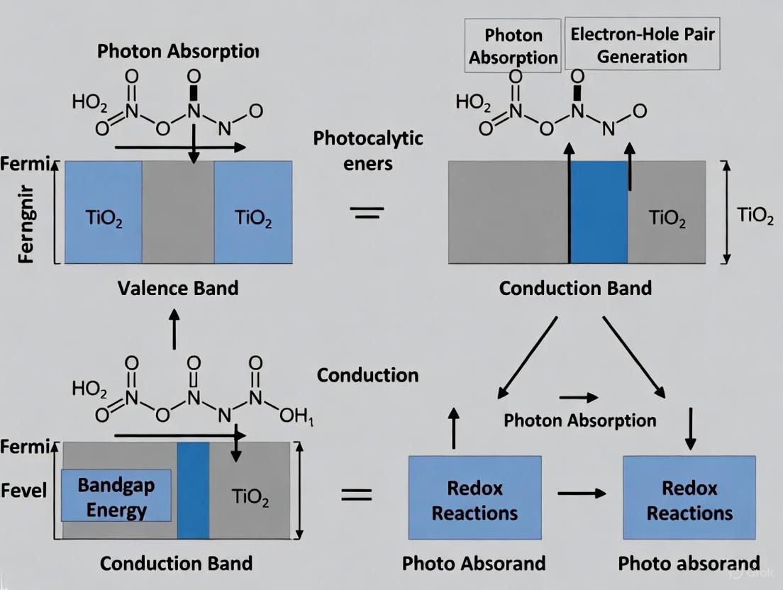
Photocatalysis represents a promising pathway for addressing global energy shortages and environmental pollution by converting solar energy into chemical energy [6] [7]. This process, pioneered by Fujishima and Honda's groundbreaking work on TiOâ‚‚ electrodes, leverages semiconductor materials to drive chemical reactions using light energy [8] [9]. At the heart of this technology lies a sophisticated sequence of events beginning with photon absorption and culminating in surface redox reactions, with charge carrier generation serving as the critical initial step that enables all subsequent processes [8] [7].
The efficiency of photocatalytic systems depends fundamentally on the properties of the semiconductor materials employed, particularly their band structure, which governs both light absorption capability and the thermodynamic potential of generated charge carriers [9]. This technical guide examines the foundational principles of the photocatalytic process, with specific focus on the mechanisms of photon absorption and charge carrier generation, framed within contemporary research on valence and conduction band engineering.
Fundamental Principles of Semiconductor Photocatalysis
Band Structure and Energy Requirements
Semiconductor photocatalysts possess a characteristic electronic structure featuring a valence band (VB) filled with electrons, a conduction band (CB) that is largely empty, and a forbidden energy region between them known as the band gap (Eð‘”) [8] [9]. When a semiconductor absorbs photons with energy equal to or greater than its band gap energy, electrons are excited from the valence band to the conduction band, creating electron-hole pairs (eâ»cb and hâºvb) [8].
For photocatalytic water splitting, the semiconductor band structure must satisfy specific thermodynamic requirements. The conduction band minimum must be more negative than the redox potential of Hâº/Hâ‚‚ (0 V vs. NHE), while the valence band maximum must be more positive than the redox potential of Oâ‚‚/Hâ‚‚O (1.23 V vs. NHE) [9]. Considering kinetic overpotentials for oxygen and hydrogen evolution reactions, the actual band gap required for unassisted photocatalytic water splitting typically exceeds 1.5 eV [9].
Table 1: Band Gap Energies and Theoretical Efficiency Limits for Selected Photocatalysts
| Photocatalyst | Band Gap (eV) | Light Absorption Edge (nm) | Theoretical STH Efficiency Limit | Primary Applications |
|---|---|---|---|---|
| Anatase TiOâ‚‚ | 3.2 [8] [9] | 388 [9] | ~1% [9] | UV-driven pollutant degradation [8] |
| Monoclinic WO₃ | 2.6 [9] | 477 [9] | ~6% [9] | Photoelectrochemical water oxidation [9] |
| α-Fe₂O₃ (Hematite) | 2.1 [9] | 590 [9] | ~15% [9] | Photoelectrochemical water splitting [9] |
| CaTiO₃ (Pristine) | 2.77 [10] | 448 [10] | - | Model perovskite photocatalyst [10] |
| S/Zr co-doped CaTiO₃ | 1.85-2.22 [10] | 560-670 [10] | Enhanced vs. pristine [10] | Visible-light water splitting [10] |
The Photocatalytic Process: A Stepwise Workflow
The fundamental photocatalytic process encompasses three primary stages: photon absorption and charge carrier generation, charge separation and migration, and surface redox reactions. The following diagram illustrates this complete workflow, with emphasis on the initial charge generation step that forms the foundation for all subsequent processes.
Diagram 1: Photocatalytic process workflow from photon absorption to surface reactions.
Photon Absorption and Charge Carrier Generation
The photocatalytic process initiates when a semiconductor absorbs photons with energy (hν) equal to or greater than its bandgap energy (Eð‘”), promoting electrons from the valence band to the conduction band [8]. This process can be represented by the fundamental equation:
TiOâ‚‚ + hν → TiOâ‚‚ (eâ»cb + hâºvb) [8]
The photogenerated charge carriers possess reductive and oxidative capacities determined by the conduction band and valence band potential of the semiconductor, respectively [8]. For TiOâ‚‚, the photogenerated holes demonstrate very high oxidative activity, enabling degradation of most organic contaminants present in water and air [8].
The timescales involved in charge carrier generation are exceptionally rapid. Interband transitions occur in the femtosecond (fs) timescale when photon energy exceeds the band gap energy [8]. Both electrons and holes then move randomly to the surface of the photocatalyst where they become trapped in the sub-picosecond time domain [8].
Band Engineering for Enhanced Light Absorption
A significant challenge in photocatalysis is that wide bandgap semiconductors like TiOâ‚‚ (3.2 eV) primarily absorb ultraviolet light, utilizing only approximately 4% of the solar spectrum [11] [6]. This limitation has stimulated extensive research into band engineering strategies to enhance visible light absorption.
Doping and heterojunction construction represent two prominent approaches for modifying band structures. For instance, doping Nb₃O₂(OH) with tantalum (Ta) or antimony (Sb) decreases the band gap from 1.7 eV (pristine) to 1.266 eV (Ta-doped) or 1.203 eV (Sb-doped), significantly enhancing visible light absorption [11]. Similarly, S/Zr co-doping in CaTiO₃ perovskite reduces the band gap from 2.77 eV to 1.85-2.22 eV while transforming the band structure from indirect to direct, further improving light absorption efficiency [10].
Quantum confinement effects provide another powerful strategy for band engineering. As demonstrated with WO₃ quantum dots, strict size control below 1.8 nm enables tuning of the conduction band edge from +0.18 VSHE to -0.10 VSHE, remarkably enhancing photoreduction of proton and molecular oxygen [12].
Table 2: Band Engineering Strategies and Their Effects on Photocatalytic Materials
| Strategy | Material System | Band Gap Modification | Effect on Photocatalytic Performance |
|---|---|---|---|
| Elemental Doping | Ta/Sb-doped Nb₃O₇(OH) | Reduction from 1.7 eV to 1.203-1.266 eV [11] | Red-shift of optical threshold to visible region [11] |
| Co-doping | S/Zr-doped CaTiO₃ | Reduction from 2.77 eV to 1.85-2.22 eV [10] | Enhanced visible light absorption for hydrogen production [10] |
| Heterojunction Construction | Cuâ‚‚O/TiOâ‚‚/Cu | Band alignment favoring charge separation [6] | Hydrogen production rate of 279.53 μmol·gâ»Â¹Â·hâ»Â¹ (25× enhancement) [6] |
| Quantum Size Effect | WO₃ quantum dots (0.66-1.79 nm) | Band gap expansion from 2.87 eV to 3.45 eV with decreasing size [12] | Upshift of CBE enables photoreduction impossible with bulk WO₃ [12] |
| Valence State Control | Cuâ‚‚O/TiOâ‚‚ vs. Cuâ‚‚O/TiOâ‚‚/Cu | Variation of Cu valence states influences band positions [6] | Different product selectivity: Hâ‚‚ production vs. CO production [6] |
Experimental Protocols for Charge Generation Studies
Synthesis of Band-Engineered Quantum Dots
Objective: Precise size control of WO₃ quantum dots to engineer conduction band position through quantum confinement effects [12].
Materials:
- Template: Supermicroporous silicas (SMPSs) with controlled pore sizes
- Precursor: Tungsten-based precursor solution
- Solvents: Appropriate solvents for precursor preparation
Methodology:
- Pore Size Selection: Choose SMPSs with specific pore sizes to determine ultimate QD dimensions
- Precursor Impregnation: Control the amount of WO₃ precursor solution impregnated into SMPSs
- In-Situ Synthesis: Form WO₃ quantum dots within the confined spaces of SMPS pores
- Characterization: Verify successful synthesis and size distribution using:
- Field Emission Transmission Electron Microscopy (FE-TEM)
- Energy Dispersive X-ray Spectroscopy (EDX)
- X-ray Photoelectron Spectroscopy (XPS) to confirm tungsten(VI) species and exclude significant Wâµâº defects [12]
Key Parameters:
- Precise control of QD size between 0.66-1.79 nm through manipulation of SMPS pore size and precursor concentration [12]
- Confirmation of narrow size distribution through FE-TEM imaging [12]
- Absence of defect absorption in UV-Vis spectra indicating minimal surface defects [12]
Conduction Band Edge Determination
Objective: Experimental evaluation of conduction band edge (CBE) potential for quantum-confined structures [12].
Materials:
- Synthesized WO₃ quantum dots
- Phenol or derivatives for surface complexation
- Spectrophotometer with UV-Vis capability
- Photoemission yield spectroscopy in air (PYSA) equipment
Methodology:
- Surface Complexation: Form complexes between WO₃-QDs and phenol
- Optical Characterization: Record absorption spectra of Cn×m/phenol complexes
- Charge-Transfer Excitation Energy: Determine ECT from Tauc plots of the complexes
- HOMO Level Reference: Establish phenol HOMO level at 1.73 VSHE using PYSA [12]
- CBE Calculation: Apply the equation: ECBE = EHOMO(phenol) - ECT [12]
Validation:
- Correlation of estimated CBE values with theoretical predictions based on effective mass approximation [12]
- Calculation of electron and hole effective masses (me = 2.39m₀, mh = 3.83m₀ for WO₃) [12]
- Confirmation that CBE upshift exceeds valence band downshift in quantum-confined systems [12]
Advanced Characterization Techniques
Understanding charge carrier dynamics requires sophisticated characterization methods that probe processes across multiple timescales. The following diagram illustrates the relationship between various characterization techniques and the specific charge transfer processes they analyze.
Diagram 2: Characterization techniques for analyzing charge carrier dynamics.
Key Characterization Methods
Transient Absorption Spectroscopy (TAS): Probes charge carrier generation and early recombination dynamics on femtosecond to nanosecond timescales, providing critical information about initial charge separation efficiency [7].
Time-Resolved Photoluminescence (TRPL): Measures charge carrier recombination rates through luminescence decay profiles, with longer lifetimes indicating reduced recombination losses [7].
Intensity-Modulated Photocurrent/Voltage Spectroscopy (IMPS/IMVS): Analyzes charge transfer and recombination kinetics in the microsecond to second range, particularly useful for photoelectrochemical systems [7].
Kelvin Probe Force Microscopy (KPFM) and Spatially Resolved Surface Photovoltage (SRSPV): Enable visualization of charge separation processes with spatial resolution, revealing localized charge trapping and transport phenomena [7].
The Scientist's Toolkit: Essential Research Reagents and Materials
Table 3: Key Research Reagents and Materials for Photocatalytic Charge Generation Studies
| Reagent/Material | Function | Application Example | Key Characteristics |
|---|---|---|---|
| Supermicroporous Silicas (SMPSs) | Template for quantum dot synthesis with controlled pore sizes [12] | Size-controlled synthesis of WO₃ quantum dots [12] | Tunable pore size, high surface area, thermal stability |
| Phenol and Derivatives | Surface complexation agents for band edge determination [12] | Experimental evaluation of conduction band edge position [12] | Charge-transfer excitation, known HOMO level (1.73 VSHE) [12] |
| DMPO (5,5-dimethyl-1-pyrroline-N-oxide) | Spin trap for radical detection in ESR spectroscopy [12] | Monitoring photoreduction of molecular oxygen via Oâ‚‚â» detection [12] | Forms stable spin adducts with superoxide radicals |
| Titanium Butoxide (Ti(OBu)â‚„) | Precursor for TiOâ‚‚ synthesis in heterojunction systems [6] | Preparation of Cuâ‚‚O/TiOâ‚‚ heterojunction photocatalysts [6] | Hydrolyzes to form TiOâ‚‚, compatible with various synthesis methods |
| Copper Acetate | Source of Cu ions for copper-based heterojunctions [6] | Synthesis of CT, CTC, and TC catalysts with different Cu valence states [6] | Transformable between Cu(I) and Cu(0) via redox processes |
| Fructose | Reducing agent in alkaline synthesis environments [6] | Mediating keto-enol tautomerism for Cu valence state control [6] | Undergoes tautomerism to glucose, which reduces copper species |
| 2,2,7-Trimethylnonane | 2,2,7-Trimethylnonane, CAS:62184-53-6, MF:C12H26, MW:170.33 g/mol | Chemical Reagent | Bench Chemicals |
| 5-Undecynoic acid, 4-oxo- | 5-Undecynoic acid, 4-oxo-, CAS:61307-46-8, MF:C11H16O3, MW:196.24 g/mol | Chemical Reagent | Bench Chemicals |
The process of photon absorption and charge carrier generation represents the fundamental initiating event in semiconductor photocatalysis, establishing the foundation upon which all subsequent efficiency depends. Through strategic band engineering approaches—including elemental doping, heterojunction construction, quantum confinement, and valence state control—researchers can precisely tune both the light absorption characteristics and the redox potential of photogenerated charge carriers. Contemporary research continues to refine our understanding of charge carrier dynamics through advanced characterization techniques capable of probing processes across femtosecond to second timescales. As band engineering strategies become increasingly sophisticated and characterization methods more precise, the rational design of high-efficiency photocatalytic systems for solar energy conversion and environmental remediation continues to advance toward practical implementation.
Semiconductor photocatalysis has emerged as a promising technology for addressing global energy and environmental challenges, including solar water splitting and pollutant degradation [1] [13]. The effectiveness of these processes fundamentally depends on the electronic band structure of the semiconductor materials employed. The band structure dictates how a material interacts with light, generates charge carriers, and facilitates redox reactions at its surface [12]. For photocatalytic reactions to occur efficiently, photoexcited electrons in the conduction band and holes in the valence band must possess sufficient energy to drive reduction and oxidation reactions, respectively [12]. This technical guide examines the key band structure parameters—specifically band edge positions and band gap widths—and their thermodynamic significance in photocatalytic systems, providing researchers with a comprehensive framework for material selection and design.
Core Band Structure Parameters
Band Gap Width and Photon Absorption
The band gap width represents the energy difference between the valence band maximum (VBM) and conduction band minimum (CBM). This parameter determines the minimum photon energy required for electron excitation and thus the portion of the solar spectrum a photocatalyst can utilize [13]. Table 1 summarizes experimental band gap values for selected photocatalytic materials.
Table 1: Band Gap Values of Selected Photocatalytic Materials
| Material | Band Gap (eV) | Light Absorption Range | Reference |
|---|---|---|---|
| NiSnO₃ sintered at 250°C | 3.38 | UV | [14] |
| NiSnO₃ sintered at 400°C | 2.90 | UV-Vis edge | [14] |
| Pristine Nb₃O₇(OH) | 1.7 | Visible | [5] |
| Ta-doped Nb₃O₇(OH) | 1.266 | Visible | [5] |
| Sb-doped Nb₃O₇(OH) | 1.203 | Visible | [5] |
| WO₃ Quantum Dots | 2.87-3.45 | UV-Vis | [12] |
| TiOâ‚‚ | ~3.0-3.2 | UV | [15] [16] |
Band gap engineering represents a crucial strategy for enhancing light absorption. Quantum confinement effects enable significant band gap tuning in nanoscale materials. For instance, WO₃ quantum dots smaller than 2 nm exhibit band gap expansion from 2.87 to 3.45 eV as particle size decreases [12]. Conversely, doping can reduce band gaps, as demonstrated by Ta and Sb doping in Nb₃O₇(OH), which decreases the band gap from 1.7 eV to 1.266 eV and 1.203 eV, respectively, red-shifting absorption into the visible region [5].
Band Edge Positions and Thermodynamic Requirements
The band edge positions relative to redox potentials determine the thermodynamic feasibility of photocatalytic reactions. The conduction band edge (CBE) must be more negative than the reduction potential of target species, while the valence band edge (VBE) must be more positive than the oxidation potential [12].
For overall water splitting, the thermodynamic minimum band gap requirement is 1.23 eV, corresponding to the water decomposition energy under standard conditions [13]. However, practical photocatalysts require additional overpotential to overcome activation energy barriers for the hydrogen evolution reaction (HER) and oxygen evolution reaction (OER) [13]. Figure 1 illustrates these thermodynamic relationships.
Figure 1. Thermodynamic requirements for photocatalytic water splitting. The conduction band must be more negative than the Hâº/Hâ‚‚ redox potential (0 V vs NHE), and the valence band must be more positive than the Hâ‚‚O/Oâ‚‚ potential (+1.23 V vs NHE). The band gap must be ≥1.23 eV.
Experimental studies have demonstrated precise band edge engineering through size control. For WO₃ quantum dots, the CBE was tuned from +0.18 V to -0.10 V vs. SHE (Standard Hydrogen Electrode) by controlling particle size below 1.8 nm, enabling photocatalytic reduction reactions previously impossible with bulk WO₃ [12]. Table 2 provides band edge positions for selected materials.
Table 2: Band Edge Positions of Photocatalytic Materials
| Material | CBE (V vs. NHE) | VBE (V vs. NHE) | Band Gap (eV) | Reference |
|---|---|---|---|---|
| WO₃ QDs (0.66-1.79 nm) | +0.18 to -0.10 | Calculated from CBE + Eg | 2.87-3.45 | [12] |
| Wâ‚‚Oâ‚„-Zn₈Wâ‚â‚€O₃₆ termination | Meets HER requirement | Meets OER requirement | Not specified | [17] |
| Theoretical minimum | ≤ 0 | ≥ +1.23 | ≥ 1.23 | [13] |
Surface termination significantly influences band edge positions. For ZnWOâ‚„(100), the Wâ‚‚Oâ‚„-Zn₈Wâ‚â‚€O₃₆ termination exhibits band edges that simultaneously fulfill HER and OER requirements, unlike other surface terminations [17]. This highlights the critical importance of surface engineering alongside bulk band structure design.
Experimental Methods for Band Structure Analysis
Theoretical Calculation Methods
Computational approaches, particularly density functional theory (DFT), provide powerful tools for predicting band structures. The Trans-Blaha modified Becke-Johnson approximation (TB-mBJ) has proven effective for calculating accurate electronic structures, outperforming standard generalized gradient approximation (GGA) methods which typically underestimate band gaps [5].
DFT Calculation Protocol:
- Structure Optimization: Perform geometric optimization using GGA functionals until residual forces on each atom are less than 0.05 eV/Ã… [15]
- Electronic Calculations: Apply TB-mBJ potential for band structure and density of states calculations [5]
- Band Alignment: Calculate work functions and band edge positions relative to vacuum level [17]
- Optical Properties: Compute frequency-dependent dielectric function to derive absorption coefficients [5]
For doped systems, spin-orbit coupling should be included to properly handle d and f orbitals of dopant atoms. Supercell approaches with appropriate dopant concentrations (e.g., 4.16% for Ta/Sb-doped Nb₃O₇(OH)) effectively model doping effects [5].
Experimental Characterization Techniques
UV-Visible Spectroscopy:
- Purpose: Determine band gap energy via Tauc plot analysis [14]
- Protocol: Measure diffuse reflectance spectra, convert to absorption data, and plot (αhν)⿠versus photon energy (hν)
- For direct band gaps: n = 1/2 [14]
- Application: Used to determine band gap reduction from 3.38 to 2.90 eV in NiSnO₃ with increased sintering temperature [14]
Photoelectron Spectroscopy:
- Purpose: Experimentally determine band edge positions [12]
- Protocol: Form surface complexes with phenol derivatives, measure charge-transfer excitation energy (ECT)
- Calculation: ECBE = EHOMO(phenol) - ECT, where EHOMO(phenol) = 1.73 VSHE [12]
- Advantage: Provides direct experimental measurement of CBE, complementary to theoretical calculations
Photocatalytic Activity Testing:
- Purpose: Validate thermodynamic feasibility of band positions [12]
- Protocol: Evaluate proton reduction and molecular oxygen reduction under UV irradiation using sacrificial reagents
- Monitoring: Employ ESR spin trapping with DMPO to detect superoxide radicals [12]
- Correlation: Relate photocatalytic efficiency to engineered CBE positions
The Scientist's Toolkit: Essential Research Reagents and Materials
Table 3: Key Research Reagents and Materials for Band Structure Studies
| Reagent/Material | Function/Application | Examples from Literature |
|---|---|---|
| Phenol/Catechol Derivatives | Form charge-transfer complexes for experimental CBE determination | WO₃-QDs/phenol complexes for CBE measurement [12] |
| Sacrificial Reagents | Consume photogenerated carriers to isolate specific redox reactions | Ethanol used as hole scavenger in WO₃ QD studies [12] |
| Spin Trapping Agents | Detect reactive oxygen species generated in reduction reactions | DMPO (5,5-dimethyl-1-pyrroline-N-oxide) for O₂•⻠detection [12] |
| Template Materials | Control nanocrystal size and quantum confinement effects | Supermicroporous silicas (SMPSs) for WO₃ QD synthesis [12] |
| Dopant Precursors | Modify band gaps and band edge positions through composition engineering | Ta and Sb precursors for Nb₃O₇(OH) doping [5] |
| 7-Methyloct-2-YN-1-OL | 7-Methyloct-2-yn-1-ol | |
| 3-(Bromomethyl)selenophene | 3-(Bromomethyl)selenophene|Research Chemical | 3-(Bromomethyl)selenophene is a key synthetic intermediate for research applications in organic electronics and materials science. For Research Use Only. Not for human or veterinary use. |
Band structure parameters—particularly band gap width and band edge positions—serve as fundamental determinants of photocatalytic activity. The precise engineering of these parameters through size control, doping, and surface termination enables the optimization of materials for specific photocatalytic applications. Experimental validation of band positions remains crucial, as theoretical predictions require correlation with measured photocatalytic performance. The continued development of sophisticated characterization techniques and computational methods will further enhance our ability to design photocatalysts with optimally tuned band structures for efficient solar energy conversion.
The escalating global energy demand and environmental degradation have driven intensive research into photocatalytic processes that convert solar energy into chemical fuels. Two of the most promising applications are photocatalytic water splitting for hydrogen production and carbon dioxide (CO2) reduction to valuable hydrocarbons. These processes rely on semiconductor materials that can absorb light and generate electron-hole pairs to drive redox reactions. The effectiveness of any semiconductor photocatalyst is fundamentally governed by its band alignment—the energy position of its valence band (VB) and conduction band (CB) relative to the redox potentials of the target reactions.
Photocatalysis operates on the principle that when a semiconductor absorbs photons with energy greater than its band gap, electrons are excited from the VB to the CB, leaving holes in the VB. These photogenerated charge carriers then migrate to the surface and participate in reduction and oxidation reactions. For a photocatalytic reaction to proceed spontaneously, the CB minimum must be more negative than the reduction potential of the target species, while the VB maximum must be more positive than the oxidation potential. This thermodynamic requirement forms the cornerstone of band alignment engineering in photocatalyst design [18] [19].
This technical guide examines the fundamental band alignment requirements for water splitting and CO2 reduction, explores strategies for engineering optimal band structures, and details experimental methodologies for characterizing and validating photocatalyst performance.
Fundamental Band Alignment Requirements
Thermodynamic Potentials for Key Reactions
The table below summarizes the essential redox potentials relative to the normal hydrogen electrode (NHE) at pH 0. These potentials define the minimum energy requirements for the conduction and valence bands of a photocatalyst.
Table 1: Standard Redox Potentials for Photocatalytic Reactions
| Reaction | Equation | Potential vs. NHE (V) | Band Requirement |
|---|---|---|---|
| Water Splitting (HER) | 2H⺠+ 2e⻠→ H₂ | 0 | CB more negative than 0 |
| Water Splitting (OER) | 2H₂O + 4h⺠→ O₂ + 4H⺠| +1.23 | VB more positive than +1.23 |
| CO₂ to CO | CO₂ + 2H⺠+ 2e⻠→ CO + H₂O | -0.53 | CB more negative than -0.53 |
| CO₂ to CH₄ | CO₂ + 8H⺠+ 8e⻠→ CH₄ + 2H₂O | -0.24 | CB more negative than -0.24 |
| CO₂ to HCOOH | CO₂ + 2H⺠+ 2e⻠→ HCOOH | -0.61 | CB more negative than -0.61 |
To drive the complete water splitting reaction without an external bias, a photocatalyst must possess a minimum band gap of 1.23 eV, in addition to satisfying the band edge positions outlined above. However, in practice, due to overpotentials and kinetic barriers, efficient photocatalysts typically require a band gap greater than 2.0 eV [19]. The band alignment for COâ‚‚ reduction is more complex due to the variety of possible products, each with distinct reduction potentials. The desired product dictates the precise CB energy level required [19].
Visualizing Band Alignment Requirements
The following diagram illustrates the fundamental band alignment requirements for a semiconductor material to be thermodynamically capable of driving both water splitting and CO2 reduction reactions.
Strategies for Engineering Band Alignment
Doping for Band Gap Tuning and Band Edge Shifting
Introducing foreign elements into a semiconductor lattice is a primary method for modifying its electronic structure. Doping can reduce the band gap to enhance visible light absorption and/or shift the band edge positions to achieve better alignment with redox potentials.
Table 2: Doping Strategies for Band Engineering
| Material | Dopant | Effect on Band Structure | Result on Photocatalytic Performance |
|---|---|---|---|
| 2D Mg(OH)â‚‚ | S, N, P | Band gap reduction from 4.82 eV to 3.86 eV (S), 3.79 eV (N), and 2.69 eV (P) [20]. | Extends light absorption into the visible range. |
| 2D Mg(OH)â‚‚ | F, Cl, SOâ‚„, POâ‚„ | Shifts valence band lower than Oâ‚‚/Hâ‚‚O oxidation potential [20]. | Renders band structure appropriate for water splitting. |
| Nb₃O₇(OH) | Ta, Sb | Band gap reduction from 1.7 eV to 1.266 eV (Ta) and 1.203 eV (Sb), with CB and VB relocation [21]. | Enhances visible-light activity and charge carrier mobility. |
The effectiveness of doping stems from the introduction of new energy levels within the band gap or the modification of the density of states of the constituent elements. For instance, in Mg(OH)â‚‚, anion doping is particularly effective because the VB maximum is primarily composed of O 2p orbitals. Replacing oxygen with elements like nitrogen creates higher-energy N 2p states above the O 2p VB maximum, thereby reducing the band gap [20].
Heterojunction Construction for Charge Separation
Combining two or more semiconductors to form a heterojunction is a powerful strategy to not only engineer band alignment but also to significantly enhance the separation of photogenerated electrons and holes, which is critical for high quantum efficiency [22].
The two most relevant heterojunction types for photocatalysis are:
- Type-II Heterojunction: The band edges are "staggered." The CB of Semiconductor B is higher (more negative) than that of Semiconductor A, while the VB of Semiconductor A is lower (more positive) than that of Semiconductor B. This alignment creates a built-in electric field that drives electrons to Semiconductor B and holes to Semiconductor A, resulting in spatial charge separation [22].
- S-Scheme Heterojunction: This is a more recent and advanced concept. It typically combines an oxidation photocatalyst (OP) with a reduction photocatalyst (RP). The internal electric field at the interface promotes the recombination of less useful electrons in the RP's CB with holes in the OP's VB. This leaves the most powerful photogenerated electrons (in the OP's CB) and holes (in the RP's VB) to participate in surface redox reactions. This mechanism preserves stronger redox potentials than a Type-II system [23].
The following diagram illustrates the charge transfer mechanisms in these two key heterojunction types.
Experimental Protocols for Characterization and Validation
Band Gap and Band Edge Determination
Accurately determining the band gap and absolute band edge positions is crucial for validating a material's potential for a specific photocatalytic reaction.
- UV-Vis-NIR Diffuse Reflectance Spectroscopy (DRS): This is the standard technique for determining the optical band gap of a powdered semiconductor. The data is typically converted to Kubelka-Munk units, and the band gap (Eg) is estimated using the Tauc plot method by plotting (F(R) * hν)^n vs. hν, where n depends on the nature of the optical transition (n=1/2 for direct and n=2 for indirect band gaps) [16].
- Mott-Schottky Analysis: This electrochemical impedance technique is performed on a working electrode made from the photocatalyst material. It is the primary method for determining the flat-band potential (Efb) of a semiconductor. For n-type semiconductors, the conduction band minimum (ECB) is typically very close (about -0.1 to -0.2 V) to Efb. For p-type semiconductors, the valence band maximum (EVB) is similarly close to Efb. The band edges can be calculated using the relationship: EVB = ECB + Eg [19].
- X-Ray Photoelectron Spectroscopy (XPS): A combined XPS and UV-Vis method can be used to determine the absolute band edge positions. The valence band spectrum from XPS provides the energy difference between the VB maximum and the Fermi level (EVB - EF). The Fermi level can be referenced using a known standard (like Au 4f). The conduction band minimum can then be calculated as ECB = EVB + E_g [20].
Photocatalytic Performance Testing
Standardized testing protocols are essential for reliably comparing the performance of different photocatalysts.
Water Splitting Test (Hâ‚‚ Evolution):
- Setup: A top-irradiation or inner-irradiation reaction vessel connected to a closed-gas circulation system.
- Procedure: Disperse 50-100 mg of photocatalyst powder in an aqueous solution (100 mL) containing a sacrificial electron donor (e.g., 10 vol% methanol or 0.1 M Na₂S/0.1 M Na₂SO₃). Evacuate the system to remove dissolved air.
- Irradiation: Use a Xe lamp (typically 300-500 W) with appropriate cut-off filters to control the wavelength (e.g., λ > 420 nm for visible light). Circulate cooling water to maintain ambient temperature.
- Analysis: The evolved gases (Hâ‚‚ and Oâ‚‚ for overall water splitting, or only Hâ‚‚ with sacrificial agents) are analyzed periodically by online gas chromatography (GC) equipped with a thermal conductivity detector (TCD) [18] [16].
COâ‚‚ Reduction Test:
- Setup: Similar to the water splitting setup, but with provisions for introducing COâ‚‚.
- Procedure: Disperse the photocatalyst in ultra-pure water in the reactor. Purity the water and reactor by repeated evacuation and purging with high-purity COâ‚‚. Finally, introduce COâ‚‚ gas to a set pressure (typically 1 atm).
- Irradiation: Use a Xe lamp with desired cut-off filters.
- Analysis: Analyze the gas phase (for products like CO, CH₄, C₂H₄) using GC-TCD/GC-FID. Analyze the liquid phase (for products like HCOOH, CH₃OH) using high-performance liquid chromatography (HPLC) or nuclear magnetic resonance (NMR) spectroscopy [19] [23].
- Control: Conduct an isotopic experiment using ¹³CO₂ to confirm the carbon source of the products is CO₂ and not residual carbon on the catalyst.
The Scientist's Toolkit: Key Research Reagent Solutions
Table 3: Essential Materials and Reagents for Photocatalysis Research
| Reagent/Material | Function/Application | Key Characteristics |
|---|---|---|
| Covalent Organic Frameworks (COFs) | Crystalline, porous organic polymer semiconductors for H₂ evolution, CO₂ reduction, and H₂O₂ production [18]. | Pre-designable structure, high surface area, π-conjugated system, functional modulability. |
| Earth-Abundant Light Absorbers (e.g., BiVO₄, Cu₂O, α-Fe₂O₃, g-C₃N₄) | Low-cost, scalable alternatives to rare/toxic semiconductors (e.g., III-V groups) for photoelectrodes [19]. | Suitable band gaps for visible light, composed of abundant elements, variable stability. |
| Sacrificial Agents (e.g., Triethanolamine (TEOA), Methanol, Na₂S/Na₂SO₃) | Electron donors (hole scavengers) used in half-reaction tests to evaluate the reduction capability of a photocatalyst [18]. | Consumes photogenerated holes, thereby suppressing charge recombination and backward reactions. |
| Co-catalysts (e.g., Pt, Ni, CoOâ‚“, NiOOH) | Nanoparticles loaded onto the photocatalyst surface to act as active sites for surface redox reactions [19]. | Lowers activation energy, enhances reaction kinetics, and in some cases aids charge separation. |
| Non-Noble Metal Cocatalysts | Sustainable and cost-effective alternative to Pt for hydrogen evolution reaction (HER) [19]. | Based on Fe, Co, Ni, Mo, W, and their compounds (sulfides, phosphides). |
| 10-Hydroxydec-6-en-2-one | 10-Hydroxydec-6-en-2-one, CAS:61448-23-5, MF:C10H18O2, MW:170.25 g/mol | Chemical Reagent |
| 5,5-Dichloro-1,3-dioxane | 5,5-Dichloro-1,3-dioxane | 5,5-Dichloro-1,3-dioxane is a chemical building block for antimicrobial and synthetic chemistry research. For Research Use Only. Not for human or veterinary use. |
The precise engineering of band alignment is a fundamental and non-negotiable aspect of developing efficient photocatalysts for water splitting and COâ‚‚ reduction. While the thermodynamic principles are well-established, the challenge lies in designing materials that simultaneously satisfy band edge requirements, possess a suitable narrow band gap for visible light absorption, and exhibit high charge separation efficiency and long-term stability. Strategies such as doping and heterojunction construction, particularly advanced concepts like S-scheme heterojunctions, provide a robust pathway to tailor the electronic structure of semiconductors. Continued advancement in precise synthetic control, coupled with sophisticated characterization techniques and theoretical modeling, is essential to bridge the gap between laboratory proof-of-concept and the large-scale, practical application of solar-driven fuel production.
Comparative Analysis of Band Structures in Common Photocatalysts (e.g., TiO2, g-C3N4)
The efficacy of semiconductor-based photocatalysis is fundamentally governed by the electronic band structure of the catalytic material. The energy difference between the valence band (VB) and the conduction band (CB), known as the band gap, along with the absolute positions of these bands, determines a photocatalyst's capacity to harvest light and drive redox reactions. This analysis provides a detailed comparison of the band structures of two predominant photocatalysts—titanium dioxide (TiO₂) and graphitic carbon nitride (g-C₃N₄)—framed within the critical context of how valence and conduction band energetics dictate photocatalytic activity and mechanisms.
Fundamental Band Structure Properties
The photocatalytic process initiates when a photon with energy greater than or equal to the semiconductor's band gap is absorbed, promoting an electron from the VB to the CB. This creates a positively charged hole in the VB. The subsequent separation and migration of these charge carriers to the surface facilitate reduction and oxidation reactions, respectively [1]. The band edge positions relative to the redox potentials of target reactions are therefore paramount.
Table 1: Fundamental Band Structure Properties of Common Photocatalysts
| Photocatalyst | Crystal Structure | Band Gap (eV) | Valence Band Position (eV vs. NHE) | Conduction Band Position (eV vs. NHE) | Primary Optical Transition |
|---|---|---|---|---|---|
| TiO₂ (Anatase) | Tetragonal | ~3.20 [24] | ~3.00 [25] | ~-0.20 [25] | O 2p → Ti 3d |
| g-C₃N₄ | Hexagonal (Graphitic) | ~2.70 [26] [27] | +1.60 [26] | -1.10 [26] | π → π* (and n → π*) |
The inherent wide band gap of anatase TiO₂ (~3.2 eV) restricts its light absorption to the ultraviolet (UV) region, which constitutes only about 5% of the solar spectrum [24]. In contrast, g-C₃N₄, with a band gap of approximately 2.7 eV, possesses a inherent visible light response [26] [27]. The VB and CB positions of g-C₃N₄ are suitably straddled for water splitting and the generation of reactive oxygen species, making it a compelling visible-light-driven photocatalyst.
Band Gap Engineering and Modulation Strategies
A primary focus of contemporary research is the engineering of photocatalyst band structures to enhance visible light absorption and improve charge separation efficiency.
Doping and Defect Engineering in TiOâ‚‚
Elemental Doping: Introducing foreign elements into the TiOâ‚‚ lattice is a prevalent method for band gap modulation.
- Cationic Doping (Metals): Doping with metals like Al³⺠can induce oxygen vacancies and alter phase stability. For instance, Al³âº/Sâ¶âº co-doping in TiOâ‚‚ has been shown to reduce the band gap from 3.23 eV to as low as 1.98 eV, significantly enhancing visible light absorption. This co-doping facilitates a phase transition from anatase to rutile, further influencing the electronic structure [28].
- Anionic Doping (Non-Metals): Nitrogen (N) is one of the most studied anionic dopants for TiOâ‚‚. N-doping can occur via substitutional or interstitial modes, leading to the formation of localized N 2p states above the O 2p VB maximum. This effectively narrows the band gap and extends absorption into the visible region up to 550 nm [25]. Other non-metals like sulfur (S) have also been employed, with their larger ionic radii creating distinct lattice distortions and band gap modifications [28].
Table 2: Band Gap Modulation in TiOâ‚‚ via Doping
| Doping Strategy | Example | Resulting Band Gap (eV) | Key Structural/Optical Changes |
|---|---|---|---|
| Metal Co-doping | Al³âº/Sâ¶âº co-doped TiOâ‚‚ | 1.98 - 3.23 (tunable) [28] | Increased rutile phase content; redshift in absorption; introduction of oxygen vacancies. |
| Non-Metal Doping | N-doped TiOâ‚‚ (N-TiOâ‚‚) | ~2.50 - 3.00 (tunable) [25] | Absorption edge extended to ~500-550 nm; formation of N 2p states above O 2p VB. |
| Single Metal Doping | Cu-doped TiOâ‚‚ | 2.28 - 3.09 (tunable) [24] | Lattice deformation; formation of oxygen vacancies and impurity states. |
Morphological and Quantum Effects: Controlling the nanoscale dimensions of photocatalysts can also tune the band structure via quantum confinement effects. For example, the conduction band edge of WO₃ quantum dots was experimentally shown to upshift as the particle size decreased below 2 nm, enabling photocatalytic reductions that are not feasible with bulk WO₃ [12]. Similar principles apply to TiO₂, where a high surface area promotes quantum confinement and enhances surface reaction kinetics [24].
Structural and Electronic Tuning of g-C₃N₄
Pore Structure Engineering: Modifying the porosity of g-C₃N₄ is an effective strategy to increase its specific surface area, providing more active sites and facilitating charge/mass transport. Synthesis methods include:
- Hard-Template Method: Yields uniform, tunable pores but requires additional steps for template removal [27].
- Soft-Template Method: Templates decompose during thermal condensation, simplifying the process but offering less control over pore regularity [27].
- Template-Free Method: The simplest approach, involving direct thermal condensation of nitrogen-rich precursors or exfoliation of bulk g-C₃N₄, though with limited improvement in specific surface area [27].
Elemental Doping and Functionalization: Doping with elements like potassium (Kâº) can redshift the Ï€-Ï€* electronic transitions in g-C₃Nâ‚„ by enhancing the planar delocalization of Ï€ electrons. Furthermore, creating a gradient band energy structure through controlled K⺠doping can significantly improve the separation efficiency of photogenerated charge carriers and their mobility to the surface [29]. Activating the inactive n-Ï€* electronic transitions by breaking the symmetrical planar structure of the heptazine units also contributes to enhanced visible light response [29].
Experimental Protocols for Band Structure Analysis
The following section outlines standard methodologies for synthesizing and characterizing the band structure of modified photocatalysts.
Objective: To prepare Al and S co-doped TiOâ‚‚ nanoparticles with enhanced visible-light photocatalytic activity.
Protocol:
- Precursor Preparation: Dissolve 2 g of titanium(III) chloride hexahydrate (TiCl₃·6H₂O) in 50 mL of deionized water and stir for 30 minutes. In a separate beaker, dissolve 0.5 g of sodium hydroxide (NaOH) in 20 mL of deionized water.
- Mixing: Add the NaOH solution dropwise to the TiCl₃ solution under magnetic stirring. Allow the mixture to stand for 10 minutes before resuming vigorous stirring for 50 minutes to ensure homogeneity.
- Hydrothermal Reaction: Transfer the resulting solution into a 100 mL Teflon-lined stainless steel autoclave. Heat the autoclave in an oven at 150°C for 24 hours.
- Washing and Drying: After reaction, cool the autoclave to room temperature. Centrifuge the resultant solution and wash the precipitate repeatedly with deionized water until the supernatant reaches pH 7. Dry the obtained pure TiO₂ nanoparticles at 60°C for 24 hours.
- Doping Introduction: For Al/S co-doping, mix Aluminum nitrate nonahydrate (Al(NO₃)₃·9H₂O) and sodium sulfate (Na₂SO₄) with TiCl₃·6H₂O in deionized water. Adjust the pH to ~9 using ammonium hydroxide to facilitate uniform precipitation.
- Calcination: Dry the gel at 100°C for 12 hours, then calcine it at 500°C for 3 hours in air to achieve crystallinity and dopant incorporation. Use a controlled heating rate of 5°C/min.
Objective: To incorporate nitrogen into the TiOâ‚‚ lattice to create a visible-light-responsive photocatalyst.
Protocol:
- Dry Methods (Sputtering): Utilize a high-vacuum chamber for sputtering a titanium target in an atmosphere of N₂/Ar or NH₃. Alternatively, oxidize pre-formed TiN at elevated temperatures.
- Wet Methods: Employ sol-gel, hydrothermal, or solvothermal processes using nitrogen-containing precursors such as urea or thiourea.
- Post-Treatment: Anneal the as-prepared materials in an ammonia or nitrogen atmosphere at temperatures typically ranging from 400°C to 600°C to facilitate nitrogen incorporation.
Determination of Band Gap and Band Edge Positions
Band Gap via UV-Vis Diffuse Reflectance Spectroscopy (DRS):
- Measure the diffuse reflectance spectrum of the powdered photocatalyst.
- Convert the reflectance data to the Kubelka-Munk function, F(R).
- Plot (F(R)*hν)⿠vs. hν (photon energy), where n = 1/2 for direct band gaps and n = 2 for indirect band gaps.
- Extrapolate the linear region of the plot to (F(R)*hν)⿠= 0 to determine the band gap energy [24].
Conduction Band Edge (CBE) Estimation via Surface Complexation:
- Form a surface complex between the semiconductor (e.g., WO₃ quantum dots) and an organic molecule with a known HOMO level, such as phenol.
- Measure the charge-transfer excitation energy (E_CT) from the absorption spectrum of the complex.
- Calculate the CBE using the equation:
E_CBE = E_HOMO(phenol) - E_CT[12]. The HOMO of phenol can be determined experimentally by techniques like photoemission yield spectroscopy in air (PYSA).
Charge Transfer Mechanisms and Heterojunction Design
Engineering heterojunctions between different semiconductors is a powerful strategy to spatially separate photogenerated electron-hole pairs, thereby inhibiting their recombination.
This diagram illustrates the charge transfer pathway in a Type-II heterojunction, a common and effective design. In such a system, the conduction and valence bands of the two semiconductors are staggered. Under light irradiation, photogenerated electrons migrate to the semiconductor with the more positive CB, while holes migrate to the semiconductor with the more negative VB. This spatial separation significantly reduces the probability of charge carrier recombination [26]. g-C₃N₄ is frequently integrated into such heterostructures with other semiconductors, including TiO₂, to enhance its photocatalytic performance.
The Scientist's Toolkit: Essential Research Reagents and Materials
Table 3: Key Reagents and Materials for Photocatalyst Research
| Reagent/Material | Function in Research | Example Application |
|---|---|---|
| Titanium Precursors (e.g., TiCl₃, Ti alkoxides) | Source of Ti for constructing the TiO₂ lattice. | Sol-gel or hydrothermal synthesis of TiO₂ nanoparticles [28] [25]. |
| Nitrogen-Rich Precursors (e.g., Urea, Melamine, Thiourea) | Source of C and N for thermal condensation into g-C₃N₄. | Thermal synthesis of bulk g-C₃N₄ [26] [27]. |
| Dopant Precursors (e.g., Al(NO₃)₃, NH₄OH, Thiourea) | Introduce foreign elements (Al, N, S) into host lattice to modify band structure. | Metal/non-metal doping of TiO₂ or g-C₃N₄ for band gap narrowing [28] [25]. |
| Structural Templates (e.g., SiO₂ nanoparticles, surfactants) | Create controlled porosity and high surface area during synthesis. | Hard- or soft-template synthesis of mesoporous g-C₃N₄ [27]. |
| Sacrificial Reagents (e.g., Methanol, Triethanolamine) | Electron donors that consume photogenerated holes, thereby enhancing reduction efficiency. | Photocatalytic hydrogen evolution experiments [29]. |
| Spin Trapping Agents (e.g., DMPO - 5,5-dimethyl-1-pyrroline-N-oxide) | Trap short-lived radical intermediates (e.g., •OOH) for detection by Electron Spin Resonance (ESR). | Mechanistic studies to confirm reactive oxygen species generation [12]. |
| 3-Butyl-1,3-oxazinan-2-one | 3-Butyl-1,3-oxazinan-2-one | 3-Butyl-1,3-oxazinan-2-one (C8H15NO2) is a versatile oxazinanone scaffold for antimicrobial and anticancer research. This product is For Research Use Only. Not for human or veterinary diagnostic or therapeutic use. |
| 3-Methoxy-2,4-dimethylfuran | 3-Methoxy-2,4-dimethylfuran|High-Purity Reference Standard | 3-Methoxy-2,4-dimethylfuran: A high-purity chemical for research use only (RUO). Explore its applications in organic synthesis and fragrance development. Not for human or veterinary use. |
The strategic engineering of band structures in TiO₂ and g-C₃N₄ is pivotal for advancing photocatalytic technology. While TiO₂ requires significant modification through doping and nanostructuring to function under visible light, g-C₃N₄ offers an inherently visible-light-active platform that can be further optimized. The choice between these materials, or their combination in heterostructures, depends on the specific redox potentials required for the target application. Future research will continue to leverage detailed band structure analysis and advanced material design to develop next-generation photocatalysts with optimized light absorption and charge separation capabilities.
Band Engineering in Action: Strategies to Tailor Materials for Enhanced Performance
Band gap engineering represents a cornerstone of modern materials science, pivotal for enhancing the efficiency of photocatalytic reactions. The strategic narrowing of a semiconductor's band gap allows for greater utilization of the solar spectrum, particularly visible light, which is a key determinant in the efficacy of photoelectrochemical cells and environmental remediation applications. This technical guide delves into the deliberate manipulation of valence and conduction band positions through elemental doping, examining two prominent material systems: Ta/Sb-doped Nb3O7(OH) and Cu-modified TiO2. By synthesizing insights from recent computational and experimental studies, this review provides a structured framework for researchers aiming to design advanced photocatalytic materials with tailored electronic structures for specific applications in energy and drug development contexts.
Theoretical Foundations: Band Structure and Photocatalysis
The Role of Valence and Conduction Bands in Photocatalysis
In semiconductor photocatalysis, the energy difference between the valence band (VB) and conduction band (CB) - the band gap - dictates the minimum photon energy required to excite an electron, creating reactive electron-hole pairs. The positions of these bands relative to redox potentials further determines the thermodynamic feasibility of catalytic reactions. For water splitting, the CB must be more negative than the Hâº/Hâ‚‚ reduction potential (0 V vs. NHE), while the VB must be more positive than the Hâ‚‚O/Oâ‚‚ oxidation potential (1.23 V vs. NHE). Doping modulates these band positions through introduced states, lattice strain, and altered orbital hybridization, enabling both improved light absorption and maintained redox power [21] [30].
Ta/Sb-Doped Nb3O7(OH): A Computational Perspective
Material System and Doping Strategy
Niobium oxide hydroxide (Nb3O7(OH)) has emerged as an attractive photocatalytic substrate due to its inherent chemical stability, suitable band positions, and abundant active sites. Recent computational studies have systematically investigated the band structure engineering of this material through doping with tantalum (Ta) and antimony (Sb), which serve as strategic isovalent and aliovalent substitutes, respectively, for niobium atoms [21].
Computational Methodology and Protocols
First-Principles Calculations: The generalized gradient approximation (GGA) was employed for structural optimization of all systems. Electronic and optical properties were calculated using the Trans-Blaha modified Becke-Johnson approximation (TB-mBJ), recognized for providing accurate band gap predictions. For the doped systems containing Ta and Sb, spin-orbit coupling was incorporated to properly account for the f and d orbitals, respectively [21].
Band Structure Analysis: The band structures, density of states, and orbital contributions were calculated using the WIEN2k code. Optical properties including the dielectric function, reflectivity, and electron energy loss function were determined with the OPTIC program [21].
Band Gap Narrowing and Electronic Structure Modifications
Doping induces significant relocation of both valence band maximum and conduction band minimum positions, effectively reducing the band gap from 1.7 eV in pristine Nb3O7(OH) to 1.266 eV with Ta doping and 1.203 eV with Sb doping. This substantial narrowing represents a reduction of approximately 25-30%, shifting the optical absorption threshold into the visible light region [21].
Table 1: Band Gap Modification in Doped Nb3O7(OH)
| Material System | Band Gap (eV) | Reduction vs. Pristine | Band Behavior |
|---|---|---|---|
| Pristine Nb3O7(OH) | 1.700 | Baseline | Direct |
| Ta-doped Nb3O7(OH) | 1.266 | 25.5% | Direct |
| Sb-doped Nb3O7(OH) | 1.203 | 29.2% | Direct |
Partial density of states analysis reveals that O p orbitals dominate the valence band, while Nb d orbitals primarily constitute the conduction band in the pristine material. Upon doping, Ta d and Sb d orbitals contribute significantly to the conduction band, modifying the electronic density and enabling lower energy transitions [21].
Transport and Optical Properties
The calculated effective mass and electrical conductivity indicate enhanced charge carrier mobility in doped systems. This improvement facilitates better separation and transport of photogenerated carriers, crucial for photocatalytic efficiency. Optical characterization demonstrates a clear red-shift in absorption edges for doped systems, confirming their enhanced visible-light responsiveness [21].
Cu-Doped TiO2: Experimental Approaches and Modifications
Material System and Synthesis Protocols
Titanium dioxide (TiOâ‚‚), particularly in the anatase phase, has been extensively studied for photocatalytic applications despite its inherent wide band gap (~3.2 eV) that limits visible light absorption. Copper doping has emerged as a prominent strategy to address this limitation through various synthesis approaches [31].
Sol-Gel Dip-Coating Synthesis: A representative experimental protocol involves dissolving tetraethyl-orthotitanate in a solution of ethanol, water, and nitric acid, followed by stirring for 1 hour and aging for 24 hours. Cu-doping is achieved by adding copper salts (e.g., Cu(NO₃)₂) to the precursor solution with concentrations typically ranging from 2-10 mol%. Film deposition is performed on glass substrates using a dip-coater at controlled withdrawal speeds (e.g., 1 mm/s), with subsequent thermal treatment to achieve crystallinity [31].
Hydrothermal Synthesis: For nanoparticle synthesis, Ti precursors such as TiCl₃·6H₂O are mixed with deionized water, followed by addition of NaOH solution under stirring. The resulting solution is transferred to a Teflon-lined autoclave and reacted at 150°C for 24 hours. Copper doping is introduced by including copper salts in the initial mixture [28].
Structural and Optical Characterization
X-ray diffraction patterns of Cu-doped TiOâ‚‚ films confirm maintenance of the anatase phase at lower Cu concentrations (<8 mol%), with no separate Cu oxide phases detected, suggesting incorporation into the TiOâ‚‚ lattice or formation of clusters below XRD detection limits. Rietveld refinements reveal lattice parameter changes indicating successful doping [31].
Optical analysis through UV-Vis spectroscopy shows significant modulation of the absorption edge. The band gap reduction follows a quantifiable relationship with Cu concentration, though the exact values depend on synthesis parameters and dopant distribution.
Table 2: Band Gap Engineering in Doped TiOâ‚‚ Systems
| Material System | Band Gap (eV) | Synthesis Method | Key Findings |
|---|---|---|---|
| Pure TiOâ‚‚ | 3.122 | Sol-gel dip-coating | Baseline [24] |
| 5 mol% Cu-doped TiO₂ (600°C) | 2.510 | Sol-gel | 19.6% reduction [24] |
| 5 mol% Cu-doped TiO₂ (700°C) | 2.430 | Sol-gel | 22.2% reduction [24] |
| Al/S co-doped TiOâ‚‚ (X4) | 1.980 | Hydrothermal | 38.7% reduction [28] |
| B-doped A-TiOâ‚‚/R-TiOâ‚‚ | Tunable | Calcination | Z-scheme heterojunction [32] |
Photocatalytic Performance Assessment
The photocatalytic activity of Cu-doped TiOâ‚‚ thin films is typically evaluated through degradation of organic dyes such as methylene blue (MB) under UV or visible light irradiation. Studies indicate that Cu-doping does not universally enhance photocatalytic activity; excessive Cu can form recombination centers (CuO, Cuâ‚‚O phases) that promote electron-hole recombination, thereby reducing quantum efficiency. The optimal dopant concentration balances band gap narrowing with minimized recombination [31].
Comparative Analysis of Doping Strategies
Mechanisms of Band Gap Narrowing
The two material systems exemplify distinct mechanisms of band gap engineering:
In Ta/Sb-doped Nb3O7(OH), doping primarily shifts both valence and conduction band positions, maintaining direct band behavior while reducing the transition energy. The Fermi level relocation facilitates electron excitation at lower energies [21].
In Cu-doped TiOâ‚‚, the band gap reduction occurs through introduction of intra-band gap states and lattice deformation, creating impurity levels within the forbidden gap that enable visible light absorption. The formation of oxygen vacancies further contributes to enhanced visible light responsiveness [31] [28].
Charge Carrier Dynamics
Both strategies aim to improve charge separation and mobility. Ta/Sb doping in Nb3O7(OH) demonstrates enhanced electrical conductivity and reduced effective mass, promoting carrier transport [21]. For Cu-doped TiOâ‚‚, the metal centers can act as both electron traps and recombination sites, depending on concentration and distribution, highlighting the importance of optimized doping parameters [31].
Advanced Engineering Strategies
Heterostructure Design
Beyond single-element doping, heterostructure engineering offers enhanced band gap control. The construction of type-II heterojunctions, such as Câ‚‚N/MSeâ‚‚ (M = Mo, W) interfaces, creates built-in electric fields that efficiently separate photogenerated carriers while maintaining strong redox potentials [33]. Similarly, boron-doped anatase/rutile TiOâ‚‚ phase junctions form direct Z-scheme heterostructures that synergistically optimize charge separation and visible light absorption [32].
Machine Learning Approaches
Recent advances incorporate machine learning for band gap prediction in doped TiO₂ systems. Gaussian process regression models utilizing lattice parameters and surface area as descriptors achieve exceptional accuracy (R² = 99.99%) in predicting band gaps, enabling high-throughput screening of doping strategies without resource-intensive computations [24].
The Scientist's Toolkit: Essential Research Reagents and Materials
Table 3: Key Research Reagents for Band Gap Engineering Studies
| Reagent/Material | Function | Application Examples |
|---|---|---|
| Tetraethyl-orthotitanate | TiOâ‚‚ precursor | Sol-gel synthesis of TiOâ‚‚ thin films [31] |
| Niobium oxide hydroxide | Photocatalyst substrate | Ta/Sb doping studies [21] |
| Tantalum pentachloride | Dopant source | Ta doping of Nb3O7(OH) [21] |
| Antimony trichloride | Dopant source | Sb doping of Nb3O7(OH) [21] |
| Copper nitrate | Dopant source | Cu doping of TiOâ‚‚ [31] |
| Boric acid | Dopant source | B doping of TiOâ‚‚ for phase junction control [32] |
| Aluminum chloride | Dopant source | Al doping of TiOâ‚‚ for co-doping studies [28] |
| Thiourea | Sulfur source | S doping of TiOâ‚‚ for co-doping studies [28] |
| Methylene blue | Photocatalytic activity probe | Degradation studies [31] |
| Rhodamine B | Photocatalytic activity probe | Degradation studies [34] |
| GTP gamma-4-azidoanilide | GTP gamma-4-azidoanilide, CAS:60869-76-3, MF:C16H20N9O13P3, MW:639.3 g/mol | Chemical Reagent |
| Oxetane;heptadecahydrate | Oxetane;heptadecahydrate, CAS:60734-82-9, MF:C3H40O18, MW:364.34 g/mol | Chemical Reagent |
The strategic doping of semiconductor materials represents a powerful approach for band gap engineering and enhanced photocatalytic performance. Ta/Sb-doped Nb3O7(OH) demonstrates precise band structure control through computational design, achieving significant band gap reductions to approximately 1.2-1.3 eV while maintaining favorable charge transport properties. Cu-doped TiOâ‚‚ illustrates the complexities of experimental implementation, where optimal doping concentrations balance visible light absorption against potential recombination losses. Emerging strategies including heterostructure design and machine learning prediction offer accelerated development pathways for next-generation photocatalytic materials. These approaches enable researchers to systematically tailor valence and conduction band positions for specific applications in environmental remediation, energy conversion, and pharmaceutical development contexts.
The imperative to address global energy shortages and environmental pollution has propelled photocatalysis to the forefront of sustainable technology research. This technology harnesses solar energy to drive chemical reactions for hydrogen production, CO2 reduction, and pollutant degradation [35]. The efficacy of any photocatalytic system fundamentally depends on the semiconductor's ability to absorb light and generate charge carriers—electrons and holes—that migrate to the surface to initiate redox reactions. A paramount challenge, however, lies in the innate tendency of these photogenerated electrons and holes to recombine, dissipating their energy as heat and drastically reducing photocatalytic efficiency [35] [36].
Single semiconductor materials, such as titanium dioxide (TiO2) and zinc oxide (ZnO), often possess inappropriate bandgap energies or rapid charge recombination rates, limiting their practical application [37] [35]. Heterojunction construction represents a powerful strategy to overcome these limitations. By forming a controlled interface between two semiconductors with distinct electronic structures, it is possible to engineer a built-in electric field that directs the spatial separation of electrons and holes, thereby inhibiting recombination [22]. This interface engineering is fundamentally governed by the alignment of valence and conduction bands at the junction, which dictates the pathway and efficiency of charge transfer. This guide provides an in-depth technical examination of two exemplary heterojunction systems—Cu2O/TiO2 and ZnS-ZnO—detailing their construction, charge transfer mechanisms, and performance in key photocatalytic applications.
Theoretical Foundations of Heterojunctions
Band Alignment Types and Charge Transfer Mechanisms
The photocatalytic performance of a heterojunction is predominantly determined by the type of band alignment at the interface, which governs the direction of charge carrier migration.
Type-II Heterojunction (Staggered Alignment): In this classic configuration, the conduction band (CB) and valence band (VB) of one semiconductor are both staggered at higher energies than those of the other. Upon light irradiation, photogenerated electrons tend to migrate to the lower-lying CB, while holes transfer to the higher-lying VB. This results in the spatial separation of charge carriers across the two materials [35] [38]. While this effectively suppresses recombination, a significant trade-off exists: the electrons and holes accumulate in energy states with reduced redox potentials, which can thermodynamically weaken their driving force for surface reactions [22] [36].
S-Scheme Heterojunction (Step-Scheme Alignment): This more advanced concept involves a reduction photocatalyst (RP) with higher Fermi level and a more negative CB, and an oxidation photocatalyst (OP) with lower Fermi level and a more positive VB [39] [40] [36]. The difference in Fermi levels causes electron transfer from RP to OP upon contact, creating an Internal Electric Field (IEF) and band bending at the interface. Under illumination, this IEF, coupled with Coulomb attraction, promotes the recombination of the useless electrons (in the OP's CB) and holes (in the RP's VB). Crucially, this process leaves the most powerful charge carriers—the electrons in the RP's CB and the holes in the OP's VB—to participate in reactions, thereby achieving efficient charge separation while preserving strong redox ability [40] [36].
Quantifying Charge Separation and Energy Losses
The efficiency of a photocatalytic process can be understood as a two-step energy conversion: first from photons to electrical energy (electron-hole pairs), and then from electrical energy to chemical energy (fuel or product) [36]. Losses occur at every stage:
- Internal Losses: These include charge carrier recombination (a major loss pathway), vibrational relaxation (thermal loss), and scattering within the semiconductor lattice [36].
- External Losses: These involve light reflection and scattering by the reactor and solution, as well as incomplete light absorption by the photocatalyst itself [36].
- Backward Reactions: The recombination of reaction products, such as H2 and O2 recombining to form water, competes with the desired forward reaction, reducing net output [36].
Heterojunctions are primarily designed to minimize internal losses by mitigating charge carrier recombination through the mechanisms described above.
Case Study I: The Cu2O/TiO2 Heterojunction System
Material Properties and Synergistic Benefits
The combination of p-type Cu2O and n-type TiO2 creates a synergistic system that addresses the weaknesses of each individual material.
Table 1: Fundamental Properties of TiO2 and Cu2O
| Property | TiO2 | Cu2O |
|---|---|---|
| Crystal Structure | Anatase (common) | Cubic |
| Band Gap (eV) | ~3.2 (UV-active) [35] | ~2.0-2.2 (Visible-light-active) [40] [35] |
| Conduction Band (CB) | More positive | More negative |
| Valence Band (VB) | More positive | More negative |
| Key Limitations | Rapid charge recombination, poor visible light absorption [35] | Photocorrosion, rapid charge recombination [39] [40] |
| Key Advantages | Strong redox ability, high stability, low cost [35] | Excellent visible light absorption, non-toxic, low cost [39] [35] |
The formation of a Cu2O/TiO2 heterojunction extends light absorption into the visible range and facilitates the separation of photogenerated electron-hole pairs, enhancing overall photocatalytic activity and stability [35].
Experimental Protocol: Constructing a Core-Shell S-Scheme Cu2O@TiO2
The following protocol details the synthesis of a Cu2O@TiO2 core-shell heterojunction for photocatalytic CO2 reduction to CH4 [39].
Primary Reagents:
- Copper(II) sulfate pentahydrate (CuSO4·5H2O): Source of Cu2+ ions.
- Sodium Hydroxide (NaOH): Provides an alkaline environment for Cu2O precipitation.
- L-Ascorbic Acid (AA): Serves as a reducing agent to convert Cu(OH)2 to Cu2O.
- Tetrabutyl Orthotitanate (TBT): Titanium precursor for TiO2 shell formation.
- Isopropyl Alcohol (IPA) & N, N'-Dimethylformamide (DMF): Solvents for the synthesis.
Synthesis Procedure:
- Synthesis of TiO2 Nanoparticles: Pre-synthesize spherical TiO2 nanoparticles.
- Dispersion of TiO2: Ultrasonically disperse the prepared TiO2 nanoparticles into a solution containing Cu2+ ions (from CuSO4·5H2O).
- Formation of Cu2O Core: Under stirring, add NaOH solution to the mixture to form Cu(OH)2. Subsequently, introduce an AA solution to reduce Cu(OH)2 and form Cu2O nanocubes. The pre-dispersed TiO2 nanoparticles assemble on the surface of the growing Cu2O, initiating the core-shell structure.
- Washing and Drying: Collect the resulting precipitate, wash it thoroughly with deionized water and ethanol, and dry it to obtain the final Cu2O@TiO2 core-shell heterojunction photocatalyst.
Charge Transfer Mechanism and Photocatalytic Performance
In the constructed S-scheme heterojunction, Cu2O acts as the RP and TiO2 as the OP [39]. The internal electric field drives the recombination of electrons in TiO2's CB with holes in Cu2O's VB. This leaves the highly reductive electrons in Cu2O's CB and the highly oxidative holes in TiO2's VB available for reactions [39] [40].
This efficient charge separation leads to remarkable performance. The optimal catalyst (Cu2O@TiO2–2) achieved production rates of 7.51 μmol hâ»Â¹ gâ»Â¹ for CH4 and 10.62 μmol hâ»Â¹ gâ»Â¹ for CO, with a high electron selectivity for CH4 of 73.9% [39]. Furthermore, introducing an interfacial nitrogen-doped carbon (NC) layer between TiO2 and Cu2O can further optimize the charge transfer pathway, switching it from a p-n to a more efficient S-scheme and enabling an exceptional H2 evolution rate of 13,521.9 μmol gâ»Â¹ hâ»Â¹ [40].
Figure 1: S-Scheme charge transfer mechanism in a Cu2O/TiO2 heterojunction. The internal electric field (IEF) promotes recombination of weaker charge carriers, leaving the most powerful electrons and holes for surface redox reactions.
The Influence of Copper Valence States
The valence state of copper in TiO2-based heterojunctions is a critical factor governing the conduction band position and product selectivity. Studies show that different copper valence states can be engineered through synthesis conditions [6].
Table 2: Effect of Copper Valence States on Photocatalytic Selectivity
| Heterojunction Type | Key Feature | Optimal Production Rate | Preferred Application |
|---|---|---|---|
| Cuâ‚‚O/TiOâ‚‚ | Dominant Cu(I) state | Hâ‚‚: 279.53 μmol gâ»Â¹ hâ»Â¹ [6] | Hydrogen Evolution Reaction (HER) |
| Cuâ‚‚O/TiOâ‚‚/Cu | Mixed Cu(I) and Cu(0) states | CO: 10.58 μmol gâ»Â¹ hâ»Â¹ [6] | COâ‚‚ Reduction to CO |
Density Functional Theory (DFT) calculations reveal that the Cu2O/TiO2 interface favors H⺠adsorption for H2 evolution, while the incorporation of metallic Cu (Cu(0)) promotes CO2 adsorption, steering the reaction pathway toward CO production [6].
Case Study II: The ZnS-ZnO Heterojunction System
Material Properties and Composite Rationale
The ZnS-ZnO heterojunction is designed to leverage the complementary properties of its constituents for applications like H2 evolution and pollutant degradation.
Table 3: Fundamental Properties of ZnS and ZnO
| Property | ZnS | ZnO |
|---|---|---|
| Crystal Structure | Cubic (Zinc Blende) | Hexagonal (Zincite) |
| Band Gap (eV) | ~3.3 - 3.8 [41] | ~3.2 - 3.44 [37] [41] |
| Key Limitations | High charge recombination, instability under light [41] | Fast charge recombination, photocorrosion, poor visible light response [37] |
| Key Advantages | Excellent transport properties, high electronic mobility [37] | Low production cost, strong redox ability [37] |
Combining ZnS and ZnO effectively separates photogenerated charge carriers, prolonging their lifetime and enhancing photocatalytic activity [37].
Experimental Protocol: Solvothermal Synthesis of ZnS-ZnO for H2 Generation
This protocol outlines the synthesis of a ZnS-ZnO heterojunction via a solvothermal method for photocatalytic H2 production [37].
Primary Reagents:
- Zinc Nitrate Hexahydrate (Zn(NO3)2·6H2O): Zinc precursor.
- Urea (NH2CONH2): Used in the preliminary synthesis of the ZnO precursor.
- Thiourea (CH4N2S): Sulfur source for ZnS formation and partial sulfidation of ZnO.
- Monoethylene Glycol (C2H6O2): Solvent for the solvothermal reaction.
Synthesis Procedure:
- Preparation of ZnO Precursor: First, synthesize a ZnO base material through the calcination of hydrozincite (Zn5(CO3)2(OH)6), which is precipitated from a zinc nitrate and urea solution.
- Solvothermal Reaction: Disperse the synthesized ZnO powder in monoethylene glycol. Add thiourea to this suspension and stir thoroughly.
- Heat Treatment: Transfer the mixture to a Teflon-lined autoclave and conduct the solvothermal reaction at a controlled temperature (e.g., 150°C, 200°C, or 250°C). The temperature is a critical parameter that determines the phase composition and crystallite size of the final heterojunction.
- Washing and Drying: After the reaction, allow the autoclave to cool naturally. Collect the resulting solid product, wash it with deionized water and ethanol, and dry it to obtain the final ZnS-ZnO heterojunction.
Charge Transfer Mechanism and Photocatalytic Performance
The heterojunction typically forms a Type-II staggered alignment. Under light irradiation, photogenerated electrons in the CB of ZnS transfer to the CB of ZnO, while holes in the VB of ZnO migrate to the VB of ZnS. This leads to the spatial separation of charge carriers, reducing recombination [37] [35]. The electrons accumulated on ZnO's surface are then available for reduction reactions, such as H⺠reduction to H2.
The photocatalytic performance is highly dependent on synthesis conditions. The ZnS-ZnO composite synthesized at 200°C demonstrated the highest hydrogen production rate of 580 μmol hâ»Â¹ gâ»Â¹ using methanol as a sacrificial agent, which was significantly higher than the performance of samples synthesized at 150°C or 250°C [37]. This was attributed to an optimal balance between ZnS and ZnO phases and an appropriate crystallite size achieved at this temperature.
The Critical Role of Surface Area and Morphology
While charge separation is crucial, surface area can be a decisive factor. A recent study on mesoporous ZnS-ZnO composites for dye degradation revealed a counter-intuitive finding: a porous ZnS sample with a high surface area (165 m² gâ»Â¹) exhibited a degradation efficiency of 88%, outperforming a ZnS-ZnO composite (55% efficiency, 35 m² gâ»Â¹) and pure ZnO (43% efficiency, 10 m² gâ»Â¹) [41]. This highlights that a high surface area provides more active sites for reactant adsorption and reaction, which can sometimes dominate over the benefits of heterojunction formation, especially in reactions where mass transport is limiting. Therefore, an ideal photocatalyst must optimize both charge separation efficiency and specific surface area.
Figure 2: Type-II charge transfer mechanism in a ZnS-ZnO heterojunction. Electrons and holes migrate in opposite directions, leading to spatial charge separation and accumulation on different semiconductors.
The Scientist's Toolkit: Essential Research Reagents
Table 4: Key Reagents for Heterojunction Synthesis and Their Functions
| Reagent | Function in Synthesis | Application Context |
|---|---|---|
| Tetrabutyl Orthotitanate (TBT) | Titanium precursor for TiOâ‚‚ synthesis | Cuâ‚‚O/TiOâ‚‚ [39] [40] |
| Copper(II) Sulfate Pentahydrate | Source of Cu²⺠ions for Cu₂O formation | Cu₂O/TiO₂ [39] [6] |
| L-Ascorbic Acid | Reducing agent for converting Cu(OH)â‚‚ to Cuâ‚‚O | Cuâ‚‚O/TiOâ‚‚ [39] [40] |
| Zinc Nitrate Hexahydrate | Zinc precursor for ZnO and ZnS formation | ZnS-ZnO [37] [41] |
| Thiourea | Sulfur source for the formation of ZnS | ZnS-ZnO [37] |
| Monoethylene Glycol | Solvent for solvothermal synthesis | ZnS-ZnO [37] |
| 2-(But-2-en-1-yl)aniline | 2-(But-2-en-1-yl)aniline, CAS:60173-58-2, MF:C10H13N, MW:147.22 g/mol | Chemical Reagent |
| 1,2,4,5-Tetrahydropentalene | 1,2,4,5-Tetrahydropentalene|C8H10| | 1,2,4,5-Tetrahydropentalene is a versatile synthetic building block and ligand scaffold for organometallic chemistry and medicinal chemistry research. For Research Use Only. Not for human or veterinary diagnostic or therapeutic use. |
The strategic construction of heterojunctions like Cu2O/TiO2 and ZnS-ZnO represents a cornerstone of modern photocatalysis research. The case studies presented herein demonstrate that interfacial engineering, which controls charge transfer pathways (e.g., S-scheme vs. Type-II), is paramount to achieving high performance. Furthermore, factors such as the valence state of metal cations and the specific surface area of the material are critically important and can dictate product selectivity and overall efficiency.
Future developments in this field are likely to focus on the precise atomic-level control of heterojunction interfaces to minimize energy losses [36]. The exploration of hybrid charge-separation strategies, which integrate the internal electric fields of AE (Asymmetric Energetics) with the fast charge-transfer kinetics of AK (Asymmetric Kinetics), also presents a promising avenue for creating next-generation photocatalysts with near-unity quantum yields [22]. As our understanding of band alignment and charge dynamics deepens, the rational design of heterojunctions will continue to be a vital tool for advancing solar energy conversion.
The rational design of valence band (VB) and conduction band (CB) structures represents a fundamental frontier in advancing photocatalytic technologies for solar fuel production and environmental remediation. In semiconductor photocatalysis, the energy levels and electronic characteristics of these bands dictate critical thermodynamic and kinetic parameters, including light absorption range, charge carrier generation, recombination rates, and ultimately, the efficiency of redox reactions at the catalyst surface [42] [43]. Organic semiconductors, particularly graphitic carbon nitride (g-C3N4) and linear conjugated polymers (CPs), have emerged as promising platforms for photocatalytic applications due to their tunable electronic structures, metal-free composition, and molecular-level design flexibility [44] [45]. Unlike their inorganic counterparts with relatively fixed band parameters, these organic semiconductors enable precise manipulation of VB and CB positions through strategic molecular engineering, creating tailored materials for specific photocatalytic reactions including COâ‚‚ reduction, hydrogen evolution, and pollutant degradation [43] [46].
The fundamental workings of organic semiconductor photocatalysis mirror processes in organic photovoltaics: light absorption leads to exciton generation, followed by exciton dissociation, charge carrier transport, and finally, charge transfer to reactant molecules [43]. The energy gap between the highest occupied molecular orbital (HOMO) and lowest unoccupied molecular orbital (LUMO)—functionally analogous to the VB and CB in inorganic semiconductors—determines the thermodynamic driving force for photocatalytic reactions [44]. This review comprehensively examines the band structure tuning strategies for two prominent organic semiconductor classes—g-C3N4 and donor-acceptor conjugated polymers—and establishes correlations between their synthetic modification, resulting electronic properties, and photocatalytic performance.
Band Structure Engineering in Graphitic Carbon Nitride (g-C3N4)
Fundamental Properties and Intrinsic Band Structure
Graphitic carbon nitride (g-C3N4) is a metal-free polymer semiconductor featuring a two-dimensional layered structure composed of tri-s-triazine or heptazine ring units connected by tertiary amines, forming an extensive in-plane π-conjugated system [45]. The material typically exhibits an optical bandgap of approximately 2.7 eV, corresponding to an absorption edge around 460 nm, with VB and CB positions at approximately +1.56 V and -1.09 V versus the normal hydrogen electrode (NHE), respectively [45]. This intrinsic band structure positions g-C3N4 favorably for various photocatalytic applications, as its CB potential provides sufficient overpotential for hydrogen evolution reaction, while its VB potential enables water oxidation and generation of reactive oxygen species [43] [45]. However, the pristine material suffers from limitations including rapid charge carrier recombination, limited visible light absorption, and relatively low surface area, which necessitate strategic band engineering to enhance its photocatalytic performance [42] [45].
Nitrogen Vacancy Engineering for Band Structure Modulation
The intentional creation of nitrogen vacancies represents a powerful strategy for tuning the electronic structure and surface properties of g-C3N4. Introducing nitrogen vacancies creates unsaturated coordination sites, adjusts the local electron density distribution, and serves as electron traps to promote the dissociation of photogenerated electron-hole pairs [42]. These modifications significantly enhance photocatalytic performance for both COâ‚‚ reduction and hydrogen evolution reactions.
A particularly effective methodology involves treating g-C3N4 with sodium hypophosphite (NHPO) as a reducing agent to generate tunable nitrogen vacancies [42]. This approach offers substantial advantages over traditional chemical redox treatments using strong oxidizing or reducing acids, as it minimizes environmental and safety concerns while effectively modifying the material's electronic properties.
Experimental Protocol: Creation of Nitrogen Vacancies via NHPO Treatment [42]
Synthesis of Pristine g-C3N4: Typically synthesized via thermal polycondensation of nitrogen-rich precursors such as melamine, dicyandiamide, or urea at 500-600°C for 2-4 hours in air.
Nitrogen Vacancy Introduction:
- Dissolve varying amounts of sodium hypophosphite (NHPO) in deionized water to create concentration gradients (e.g., 5%, 8%, 11% NHPO solutions).
- Disperse g-C3N4 powder in the NHPO solutions under continuous stirring.
- Heat the mixture at 60-80°C for several hours to facilitate the reduction process.
- Collect the modified g-C3N4 by centrifugation, wash thoroughly with deionized water, and dry at 60°C overnight.
Material Characterization:
- XRD Analysis: Confirm retention of primary crystal structure with characteristic peaks at 13.1° (100) and 27.3° (002).
- FTIR Spectroscopy: Identify chemical bond components and confirm structural integrity after modification.
- ESR Spectroscopy: Directly detect and quantify nitrogen vacancies via characteristic signals.
- UV-Vis DRS: Measure enhanced light absorption and bandgap narrowing.
- XPS Analysis: Determine elemental composition and chemical states, confirming nitrogen deficiency.
Photocatalytic Testing:
- COâ‚‚ Reduction: Suspend catalyst in COâ‚‚-saturated aqueous solution under 300 W Xe lamp irradiation; quantify products (CO, CHâ‚„) via gas chromatography.
- Hâ‚‚ Evolution: Disperse catalyst in aqueous solution containing sacrificial electron donors (e.g., triethanolamine); measure evolved Hâ‚‚ using gas chromatography.
The incorporation of nitrogen vacancies through this methodology significantly enhances photocatalytic performance. Optimal NHPO-treated g-C3N4 (11NHPO-CN) exhibits CO and CHâ‚„ production rates of 9.12 μmol·gâ»Â¹Â·hâ»Â¹ and 0.84 μmol·gâ»Â¹Â·hâ»Â¹, respectively, representing a four-fold increase compared to unmodified g-C3N4 [42]. Similarly, photocatalytic hydrogen evolution rates show substantial improvement. These enhancements originate from multiple factors: nitrogen vacancies create mid-gap states that narrow the effective bandgap and extend visible light absorption; they function as electron traps to suppress charge carrier recombination; and they provide additional active sites for reactant adsorption and surface reactions [42].
Heterojunction Construction and Elemental Doping
Beyond vacancy engineering, g-C3N4's band structure can be effectively modulated through heterojunction formation with other semiconductors and elemental doping. Constructing heterostructures with materials such as TiOâ‚‚, CuO, BiOX, or metal-organic frameworks (MOFs) enables improved charge separation through built-in electric fields at interfaces [42] [45]. Similarly, doping with main group elements (B, S, P) or transition metals (Fe, Co, Ni) introduces discrete energy states within the bandgap, modifying both light absorption characteristics and charge carrier dynamics [45]. These approaches collectively contribute to enhanced photocatalytic performance by facilitating the critical processes of light harvesting, charge separation, and surface reactions.
Band Structure Tuning in Donor-Acceptor Conjugated Polymers
Molecular Design Principles for Band Structure Control
Conjugated polymers (CPs) represent a versatile class of organic semiconductors whose band structures can be precisely engineered at the molecular level through strategic selection of electron-donating (D) and electron-accepting (A) building blocks [44] [43]. The fundamental design principle involves creating alternating D-A configurations along the polymer backbone, where the HOMO energy level is primarily governed by the electron-donating unit, while the LUMO energy level is dominated by the electron-accepting unit [44]. This molecular-level control enables fine-tuning of the HOMO-LUMO gap (equivalent to VB-CB gap), light absorption characteristics, and redox potentials for targeted photocatalytic applications.
Recent advances have demonstrated that cyanostyrylthiophene (CST)-based D-A conjugated polymers serve as excellent platforms for photocatalytic hydrogen evolution [44]. Systematic variation of the electron-accepting units—including pyridine, thiophene, benzene, naphthalene, and methylbenzene derivatives—enables precise modulation of the polymers' optoelectronic properties and photocatalytic performance [44]. The planarity and steric hindrance of these building blocks further influence the overall conjugation, molecular packing, and charge transport properties, creating additional parameters for performance optimization.
Synthetic Methodology and Structural Characterization
The synthesis of high-performance D-A conjugated polymers employs sophisticated polymerization techniques that ensure controlled structure and optimal electronic properties.
Experimental Protocol: Direct C-H Arylation Polymerization (DArP) of CST-Based Conjugated Polymers [44]
Monomer Synthesis (Knoevenagel Condensation):
- React equimolar amounts of bromo-substituted aromatic aldehydes with 2-(thiophen-2-yl)acetonitrile (Th-ACN) in ethanol or methanol.
- Catalyze the reaction with a base such as piperidine or sodium ethoxide.
- Heat under reflux for 6-12 hours with continuous stirring.
- Collect the precipitated CST-based monomers (CST-BPD, CST-BT, CST-BP, CST-BN, CST-BMP) via filtration and purify through recrystallization.
Polymerization via Direct C-H Arylation:
- Dissolve CST monomers and catalytic system in dry, degassed solvent (e.g., DMF, toluene).
- Employ palladium catalysts (e.g., Pd(OAc)₂, Pd₂(dba)₃) with appropriate ligands (e.g., P(o-MeOPh)₃, PCy₃·HBF₄).
- Add silver or cesium carbonate as base to facilitate deprotonation.
- Heat reaction mixture at 80-120°C for 24-48 hours under inert atmosphere.
- Terminate polymerization by cooling and pouring into methanol.
- Collect precipitated polymers (CP1-CP5) via filtration and purify through sequential Soxhlet extraction with methanol, acetone, and chloroform.
Structural and Electronic Characterization:
- FTIR Spectroscopy: Confirm preservation of key functional groups (C=C at ~1640 cmâ»Â¹, -CN at ~2232 cmâ»Â¹).
- X-ray Crystallography: Determine molecular geometry and dihedral angles of monomer units.
- DFT Calculations: Predict optimal geometries, dihedral angles, and frontier molecular orbital distributions.
- UV-Vis Spectroscopy: Measure absorption spectra and estimate HOMO-LUMO gaps.
- Photoluminescence Spectroscopy: Assess charge recombination behavior.
- Transient Photocurrent Response: Evaluate charge separation efficiency.
- Cyclic Voltammetry: Determine HOMO/LUMO energy levels relative to vacuum.
Photocatalytic Hydrogen Evolution Testing:
- Disperse conjugated polymer photocatalyst (5-20 mg) in aqueous solution containing ascorbic acid as sacrificial electron donor.
- Illuminate with visible light source (λ > 420 nm) with continuous stirring.
- Quantify evolved hydrogen gas using gas chromatography at regular intervals.
- Calculate hydrogen evolution rate (HER) as mmol H₂·hâ»Â¹Â·gâ»Â¹.
The photocatalytic performance of these systematically designed conjugated polymers reveals strong structure-property-activity relationships. Among the CST-based polymers, CP3 (incorporating phenyl-cyanostyrylthiophene) demonstrates superior hydrogen evolution rate of 7.60 mmol·hâ»Â¹Â·gâ»Â¹, significantly outperforming other structural variants [44]. This enhanced performance correlates with optimal dihedral angles between donor and acceptor units, favorable molecular planarity for efficient charge transport, and balanced HOMO-LUMO positions that provide sufficient thermodynamic driving force while maintaining visible light absorption [44].
Table 1: Photocatalytic Performance of Modified g-C3N4 and Conjugated Polymers
| Material Class | Specific Modification | Photocatalytic Reaction | Performance Metrics | Reference |
|---|---|---|---|---|
| g-C3N4 | Nitrogen vacancies (11NHPO-CN) | COâ‚‚ Reduction | CO: 9.12 μmol·gâ»Â¹Â·hâ»Â¹, CHâ‚„: 0.84 μmol·gâ»Â¹Â·hâ»Â¹ | [42] |
| g-C3N4 | Nitrogen vacancies (11NHPO-CN) | Hâ‚‚ Evolution | Significant rate increase vs. pristine g-C3N4 | [42] |
| Conjugated Polymer CP3 | Phenyl-cyanostyrylthiophene backbone | Hâ‚‚ Evolution | 7.60 mmol·hâ»Â¹Â·gâ»Â¹ | [44] |
Comparative Analysis: Band Structure Tuning Strategies and Performance
The strategic manipulation of band structures in g-C3N4 and conjugated polymers, while sharing the common goal of enhancing photocatalytic efficiency, employs distinct approaches rooted in their respective material architectures. g-C3N4 modification primarily occurs through post-synthetic treatments that alter the existing framework—creating nitrogen vacancies, introducing dopant atoms, or forming composite interfaces [42] [45]. In contrast, conjugated polymer band structures are typically pre-designed through molecular engineering prior to synthesis, selecting specific donor and acceptor units to achieve target HOMO-LUMO positions [44] [43]. Both approaches demonstrate remarkable effectiveness in optimizing the critical processes in photocatalysis: light harvesting, charge separation, and surface reactions.
Table 2: Band Structure Tuning Mechanisms in Organic Semiconductors
| Material System | Primary Tuning Strategies | Effects on Band Structure | Impact on Photocatalytic Processes |
|---|---|---|---|
| g-C3N4 | Nitrogen vacancy engineering | Creates mid-gap states, narrows effective bandgap, enhances visible light absorption | Improves charge separation, creates active sites, enhances COâ‚‚ adsorption and reduction |
| g-C3N4 | Heterojunction construction | Forms interfacial electric fields, alters band bending | Facilitates spatial charge separation, reduces recombination losses |
| g-C3N4 | Elemental doping | Introduces discrete energy levels within bandgap | Extends light absorption range, modifies charge carrier dynamics |
| Conjugated Polymers | Donor-acceptor architecture | Precisely controls HOMO/LUMO positions through molecular design | Optimizes redox potentials for specific reactions, enhances light absorption |
| Conjugated Polymers | Side chain functionalization | Modifies surface properties without significantly altering backbone electronics | Improves dispersibility, enhances interfacial contact with reactants |
| Conjugated Polymers | Conjugation length modulation | Affects delocalization of π-electrons | Influences charge carrier mobility and light absorption characteristics |
Functional group modifications represent another powerful strategy for fine-tuning the electronic properties of organic semiconductors. Specific functional groups impart distinct effects on photocatalytic performance: electron-regulating groups (cyano, halogen) induce molecular dipoles that facilitate photogenerated electron migration; π-conjugated extension groups (anthraquinone, thiophene) expand conjugation and improve visible light capture; hydroxyl groups enhance surface hydrophilicity and promote water activation; while multi-active site functional groups (sulfonic acid, amide) accelerate reaction kinetics and inhibit product decomposition [47]. These molecular-level modifications demonstrate the exquisite control possible over organic semiconductor properties through rational chemical design.
The Scientist's Toolkit: Essential Research Reagents and Materials
Table 3: Key Research Reagents for Organic Semiconductor Synthesis and Modification
| Reagent/Material | Function in Research Context | Application Examples |
|---|---|---|
| Sodium Hypophosphite (NHPO) | Reducing agent for creating nitrogen vacancies | Nitrogen vacancy engineering in g-C3N4 [42] |
| 2-(Thiophen-2-yl)acetonitrile | Electron-accepting monomer for conjugated polymer synthesis | Building block for CST-based conjugated polymers [44] |
| Palladium Catalysts (e.g., Pd(OAc)â‚‚) | Catalyst for direct C-H arylation polymerization | Facilitating C-C bond formation in conjugated polymer synthesis [44] |
| Bromo-substituted Aromatic Aldehydes | Electron-donating monomers with reactive sites for polymerization | Varied building blocks for D-A conjugated polymers (pyridine, thiophene, benzene derivatives) [44] |
| Melamine, Dicyandiamide, Urea | Nitrogen-rich precursors for g-C3N4 synthesis | Thermal polycondensation to form graphitic carbon nitride [45] |
| Ascorbic Acid | Sacrificial electron donor in photocatalytic testing | Consuming photogenerated holes to facilitate hydrogen evolution reaction [44] |
| 8-Methylnonane-2,5-dione | 8-Methylnonane-2,5-dione|C10H18O2|RUO | 8-Methylnonane-2,5-dione (C10H18O2) is a high-purity reagent for flavor and fragrance research. This product is for research use only (RUO). Not for personal use. |
| 2-Hydroxypent-2-enoic acid | 2-Hydroxypent-2-enoic acid, CAS:60976-08-1, MF:C5H8O3, MW:116.11 g/mol | Chemical Reagent |
The strategic engineering of band structures in g-C3N4 and conjugated polymers represents a cornerstone in advancing organic semiconductor photocatalysis. Through nitrogen vacancy creation, heterojunction formation, molecular-level donor-acceptor design, and functional group modifications, researchers can precisely tailor the electronic properties of these materials to optimize their performance for specific photocatalytic applications including COâ‚‚ reduction, hydrogen evolution, and environmental remediation [42] [44] [45]. The continued development of these tunable organic semiconductors promises to play a pivotal role in addressing global energy and environmental challenges through solar-driven chemical transformations.
Future research directions will likely focus on enhancing the stability of organic semiconductors under operational conditions, developing more sustainable synthesis pathways, and integrating computational approaches such as machine learning to identify optimal material combinations and modification strategies [43] [47]. As fundamental understanding of structure-property-activity relationships deepens, the exquisite control over valence and conduction band characteristics in organic semiconductors will unlock new frontiers in photocatalytic technology for sustainable energy conversion and environmental protection.
The efficiency of photocatalytic reactions, pivotal for energy generation and environmental remediation, is fundamentally governed by the interplay between a semiconductor's electronic structure and its physical architecture. The energy positions of the valence band (VB) and conduction band (CB) determine the thermodynamic feasibility of redox reactions, such as water splitting and pollutant degradation [48]. However, the practical realization of this potential is critically dependent on two intertwined material properties: the accessible surface area for reactant adsorption and the efficiency of charge carrier pathways from the bulk to the reactive interface. Nanostructuring and surface engineering have emerged as powerful strategies to simultaneously optimize both aspects. By manipulating material dimensions at the nanoscale and rationally designing surface states, researchers can dramatically increase the density of active sites while managing the complex dynamics of photogenerated electrons and holes. This guide examines the profound impact of these strategies on photocatalytic efficiency, providing a technical framework for researchers and scientists to design advanced photocatalytic systems, with a consistent focus on the role of band structure in directing surface reactions.
Fundamental Principles of Photocatalysis and Band Structure
At its core, heterogeneous photocatalysis is initiated by the absorption of a photon with energy equal to or greater than the semiconductor's band gap ((E_g)), promoting an electron ((e^-)) from the valence band to the conduction band and creating a hole ((h^+)) in the valence band [49]. This generates an electron-hole pair, as described by:
[ \text{SC} + h\nu \rightarrow e^-{\text{CB}} + h^+{\text{VB}} ]
The subsequent processes—separation, migration, and surface reaction of these charge carriers—are what ultimately determine photocatalytic efficiency. The energy difference between the band edges and the redox potentials of target molecules (e.g., H₂O/H₂, O₂/H₂O, or organic pollutants) dictates the thermodynamic driving force for the reaction [48]. For instance, a semiconductor's conduction band minimum (CBM) must be higher (more negative) than the hydrogen reduction potential (H₂/H₂O) for hydrogen evolution, while its valence band maximum (VBM) must be lower (more positive) than the water oxidation potential (O₂/H₂O) for oxygen evolution.
The primary challenge lies in the transient nature of photogenerated carriers. They can undergo radiative or non-radiative recombination, dissipating their energy as heat or light, which severely diminishes catalytic activity. The probability of recombination increases with the distance carriers must travel to reach the surface. In bulk materials, this distance is significant, and most carriers recombine before participating in surface chemistry. Nanostructuring directly addresses this by shortening the migration pathway, thereby enhancing the probability that charges will reach the surface.
Table 1: Key Electronic Properties Governing Photocatalytic Activity
| Property | Description | Influence on Photocatalysis |
|---|---|---|
| Band Gap ((E_g)) | Energy difference between VB and CB. | Determines the range of utilizable solar spectrum; a smaller (E_g) absorbs more visible light. |
| Band Edge Positions | Absolute energy levels of CBM and VBM. | Must straddle the redox potentials of the target reaction for thermodynamic feasibility. |
| Charge Carrier Density | Concentration of photogenerated (e^-)/(h^+) pairs. | A higher density increases the probability of surface reactions but can also accelerate recombination. |
| Charge Carrier Lifetime | The average time (e^-) and (h^+) remain separated. | A longer lifetime provides a greater opportunity for charges to migrate to the surface and initiate reactions. |
Impact of Nanostructuring on Surface Area and Charge Pathways
Enhancement of Specific Surface Area
Nanostructuring inherently increases the specific surface area of a photocatalytic material. A higher surface area provides a greater number of active sites for the adsorption of reactant molecules and the subsequent catalytic turnover [41]. The synthesis of porous architectures is a particularly effective nanostructuring strategy, as it creates intricate networks of channels and pores that further enhance light harvesting through internal reflection and scattering, while facilitating molecular transport [41].
The decisive role of surface area was starkly demonstrated in a 2025 study comparing porous ZnS, ZnO, and a ZnS-ZnO heterostructure [41]. Despite ZnS having a wider band gap and lower intrinsic charge carrier density than the composite, its significantly higher surface area resulted in superior photocatalytic performance for methylene blue degradation.
Table 2: Quantitative Comparison of Porous ZnS-based Photocatalysts
| Photocatalyst | Specific Surface Area (m²/g) | Band Gap (eV) | Charge Carrier Density (cmâ»Â³) | Dye Removal Efficiency (%) |
|---|---|---|---|---|
| Porous ZnS | 165 | 3.3 | (9.21 \times 10^{15}) | 88 |
| ZnS-ZnO Composite | 35 | Not Specified | Not Specified | 55 |
| Porous ZnO | 10 | Not Specified | Not Specified | 43 |
This data underscores that while electronic properties are crucial, a high specific surface area can be a dominating factor for performance, as it ensures that a greater proportion of the generated charges can interact with adsorbates.
Shortening of Charge Carrier Pathways
The primary electronic benefit of nanostructuring is the reduction in the distance that photogenerated charge carriers must travel to reach the surface. In bulk materials, this distance can be on the order of micrometers, and the probability of recombination is high. In nanoparticles or mesoporous structures, this pathway is shortened to nanometers, significantly increasing the likelihood of charges reaching the interface before recombining [50]. This effect is often coupled with the quantum confinement observed in very small nanoparticles (<10 nm), which can cause a blue shift in the absorption edge and enhance the redox potential of charge carriers [49].
A critical debate in the field has centered on whether the high surface area of nanostructures introduces additional surface recombination sites, thereby counteracting the benefits of short migration pathways. However, ultrafast transient absorption spectroscopy studies on TiOâ‚‚ films have revealed that nanostructuring does not enhance recombination rates on ultrafast timescales [50]. The recombination kinetics in mesoporous and dense films were found to be qualitatively similar for both anatase and rutile polymorphs, indicating that surface state-mediated recombination is not a dominant loss pathway and that bulk recombination remains the primary determinant of charge carrier lifetime [50]. This finding validates the strategy of nanostructuring for improved charge utilization.
Surface Engineering for Enhanced Charge Separation and Transport
While nanostructuring provides physical access to the surface, surface engineering chemically and electronically modifies the interface to further improve charge separation and direct surface reactions. Key strategies include heterojunction formation, defect engineering, and molecular functionalization.
Heterojunction Formation and Band Alignment
Creating interfaces between different semiconductors (heterojunctions) is a powerful method to manipulate charge flow. In a type-II heterojunction, the band alignment is staggered such that the CB and VB of one semiconductor are both higher than those of the other. This creates a built-in potential that drives electrons to one side and holes to the other, effectively spatially separating the charge carriers and drastically reducing recombination [41]. The ZnS-ZnO composite studied is an example of such a system, where the heterostructure is designed to reduce electron-hole pair recombination by transferring charge carriers to surface defects [41].
Defect Engineering and Surface States
The role of surface states is complex and dual-edged. On one hand, they can act as recombination centers, trapping both electrons and holes and facilitating their annihilation. On the other hand, they can serve as beneficial trapping sites that temporarily localize a single type of carrier (electron or hole), preventing its recombination and facilitating its transfer to an adsorbate [50]. The beneficial role of defects was evident in the porous ZnS study, where visible-range emissions and Mott-Schottky analysis confirmed that defect states enhanced charge separation under LED illumination [41]. Therefore, careful surface engineering to introduce a controlled density of beneficial defects, while passivating detrimental ones, is a key aspect of photocatalyst design.
Aqueous Environment and Band Edge Shifts
For photocatalysis in aqueous environments, such as water splitting or water purification, the interaction between the catalyst surface and water molecules cannot be ignored. Traditional calculations often assume a rigid shift of the band edges due to water. However, advanced DFT simulations involving thousands of atoms reveal that the CBM and VBM of two-dimensional photocatalysts like MoSâ‚‚, GaS, and InSe can shift by different values in the presence of water [48]. These non-rigid shifts are critical for accurately determining the thermodynamic driving force for reactions and are governed by several factors:
- Geometric Deformation: Water adsorption can induce structural changes in the catalyst.
- Water Dipole Potential: The ordered structure of water molecules at the interface creates an electrostatic potential.
- Charge Redistribution: Electron density shifts at the solid-liquid interface.
- Interfacial Chemical Contact: Hybridization between catalyst atoms and water molecules, which particularly affects the VBM in materials with out-of-plane orbitals [48].
This understanding is essential for the rational selection and design of photocatalysts for aqueous applications, as it can reveal, for instance, an upward CBM shift that thermodynamically favors the hydrogen evolution reaction [48].
Quantitative Analysis of Surface-Reaching Charges
A significant challenge in photocatalysis research is moving beyond the measurement of bulk charge generation to the quantitative assessment of charges that actually reach the surface, as these are the only species that can participate in chemical reactions. The scarcity of these surface-reaching charges is a major bottleneck [51].
The Methanol Surface Elementary Reaction Kinetic Analysis Method
A robust methodology for quantifying surface-reaching holes, specifically for TiOâ‚‚-based systems, involves the kinetic analysis of methanol photo-oxidation [51]. Methanol acts as a sacrificial hole scavenger, and its oxidation kinetics are directly proportional to the concentration of holes at the surface.
Experimental Protocol:
- Catalyst Preparation and Characterization: Synthesize and characterize the TiOâ‚‚ photocatalyst (e.g., anatase nanocrystals with dominant {001}, {101} facets) using XRD, BET surface area analysis, and TEM.
- Adsorption Setup: Introduce a controlled, sub-monolayer quantity of methanol vapor into a sealed reaction chamber containing the catalyst, allowing it to reach adsorption equilibrium in the dark. Molecular methanol (CH₃OH(a)) adsorbs at fivefold-coordinated Tiâµâº sites, while dissociative adsorption forms methoxy species (CH₃O(a)) at defect sites [51].
- Photocatalytic Reaction: Illuminate the system with a standardized light source (e.g., UV LED) of known intensity. Monitor the reaction products in real-time using mass spectrometry or gas chromatography.
- Kinetic Analysis: The initial rate of formaldehyde (HCHO) production is directly measured. This rate is linked to the surface hole concentration (([h^+]{surf})) through the kinetic order of the reaction. The methodology is based on the established mechanism where methoxy species are oxidized by holes: [ \text{CH}3\text{O}^- + h^+ \rightarrow \cdot\text{CH}_3\text{O} \rightarrow \text{HCHO} + \text{H}^+ + e^- ] By measuring the reaction rate under controlled conditions, one can back-calculate the concentration of holes available at the surface to drive this reaction [51].
This method has been successfully applied to correlate surface-reaching hole density with performance enhancements from various surface engineering strategies, such as crystal facet control, doping, and defect engineering [51].
The Scientist's Toolkit: Essential Reagents and Materials
Table 3: Key Research Reagent Solutions for Photocatalyst Synthesis and Evaluation
| Reagent/Material | Function/Application | Specific Example |
|---|---|---|
| Zinc Nitrate Hexahydrate | Metal precursor for the synthesis of Zn-based photocatalysts. | Used as a zinc source in the facile synthesis of porous ZnS and subsequent oxidation to ZnO [41]. |
| Sodium Sulfide Pentahydrate | Sulfur precursor for the synthesis of metal sulfide photocatalysts. | Reacted with zinc nitrate in ethanol to form porous ZnS nanostructures [41]. |
| Methanol (CH₃OH) | Sacrificial hole scavenger and probe molecule for surface reaction kinetics. | Used in the adsorbate surface elementary reaction kinetic analysis method to quantify surface-reaching photoholes on TiO₂ surfaces [51]. |
| Methylene Blue | Model organic pollutant for evaluating photocatalytic degradation efficiency. | Degraded under LED illumination to benchmark the performance of porous ZnS, ZnO, and ZnS-ZnO photocatalysts [41]. |
| Oxygen (Oâ‚‚) | Electron scavenger and reactant in oxidation reactions. | Critical for promoting methanol photodecomposition, scavenging electrons to maintain charge separation, and participating in surface intermediate reactions during photocatalysis [51]. |
| 4-Methoxy-4'-pentylbiphenyl | 4-Methoxy-4'-pentylbiphenyl | C18H22O | CAS 58244-49-8 |
Nanostructuring and surface engineering are complementary and indispensable strategies for advancing photocatalytic technology. Nanostructuring primarily addresses kinetic challenges by dramatically increasing the surface area and shortening the migration pathways for charge carriers, thereby increasing their probability of participating in surface reactions. Surface engineering, through heterojunctions, defects, and chemical modification, addresses electronic and thermodynamic challenges by enhancing charge separation, tuning band edge positions, and controlling surface reactivity. The integration of these approaches, guided by advanced characterization methods like surface kinetic analysis and ultrafast spectroscopy, allows for the rational design of high-efficiency photocatalysts. The continued refinement of these strategies, with a deepened understanding of the solid-liquid interface, is essential for unlocking the full potential of photocatalysis in sustainable energy and environmental applications.
The global energy crisis and environmental challenges have intensified the search for sustainable solutions, with semiconductor photocatalysis emerging as a promising technology for renewable energy generation and environmental remediation. [52] [53] At the heart of photocatalytic efficiency lies a fundamental electronic property: the band structure of semiconductor materials, specifically the energy relationship between valence and conduction bands. The capacity to accurately predict and engineer these band structures is thus paramount for advancing photocatalytic research.
Density Functional Theory (DFT) has established itself as an indispensable computational tool in this endeavor, enabling researchers to probe the electronic, optical, and structural properties of photocatalytic materials before embarking on costly and time-consuming synthetic pathways. [53] [54] This technical guide provides an in-depth examination of how DFT calculations are employed to model band structures and predict the photocatalytic properties of materials, with a specific focus on the critical role of valence and conduction bands in driving photocatalytic reactions.
Theoretical Foundations of Photocatalysis and Band Structure
The Photocatalytic Process and Band Theory
Photocatalysis is a process where a semiconductor material, the photocatalyst, uses light energy to accelerate a chemical reaction without being consumed itself. [53] The fundamental mechanism is governed by the principles of band structure theory in solid-state physics. [53]
When a photocatalyst absorbs a photon with energy equal to or greater than its band gap (E₉) - the energy difference between the valence band (VB) and conduction band (CB) - an electron (eâ») is excited from the VB to the CB, leaving behind a positively charged hole (hâº). This generates an electron-hole pair, as described by Equation 1: [52]
(Equation 1)
The resulting charge carriers then migrate to the catalyst surface where they drive reduction and oxidation reactions. The potential energy of these carriers is dictated by the relative positions of the CB and VB edges. [52] For a photocatalytic reaction like water splitting to proceed spontaneously, the CB minimum must be more negative than the Hâº/Hâ‚‚ reduction potential (0 V vs. NHE at pH=0), while the VB maximum must be more positive than the Hâ‚‚O/Oâ‚‚ oxidation potential (1.23 V vs. NHE). [52] This establishes a thermodynamic requirement for the photocatalyst band gap of at least 1.23 eV.
The Critical Role of Valence and Conduction Bands
The valence band represents the highest range of electron energies in which electrons are present at absolute zero, essentially comprising the bound electrons that participate in chemical bonding. [52] The conduction band is the lowest range of vacant electronic states where electrons can move freely through the material, enabling electrical conductivity. [52] The interaction between these bands and their respective band edges dictates photocatalytic efficiency through several key factors:
- Charge Carrier Generation: The probability of electron-hole pair formation depends on the band gap magnitude and the nature of the optical transitions between VB and CB. [53]
- Redox Potential: The absolute positions of VB and CB edges relative to reactant energy levels determine whether the photogenerated carriers possess sufficient potential to drive desired reactions. [52]
- Charge Separation and Recombination: The spatial separation of VB and CB, along with their dispersion characteristics, influences the likelihood of electron-hole recombination versus their migration to active sites. [53]
Table 1: Key Band Structure Parameters and Their Impact on Photocatalytic Activity
| Parameter | Description | Impact on Photocatalysis |
|---|---|---|
| Band Gap (E₉) | Energy difference between VB maximum and CB minimum | Determines the range of absorbable light spectra; must be sufficient to drive the reaction but small enough to utilize visible light |
| Band Edge Positions | Absolute energy levels of VB and CB relative to vacuum level | Dictates the thermodynamic feasibility of redox reactions; must straddle the reaction potentials |
| Band Structure Type | Direct vs. indirect band gap | Affects the probability of optical transitions and carrier recombination rates |
| Effective Mass | Curvature of VB and CB dispersion | Influences carrier mobility and migration efficiency to surface reaction sites |
| Density of States | Number of available electronic states at each energy level | Affects light absorption efficiency and the number of available charge carriers |
DFT Methodologies for Band Structure Prediction
Fundamental DFT Approaches
Density Functional Theory provides a computational framework for solving the many-body Schrödinger equation by focusing on electron density rather than wavefunctions. [53] The accuracy of DFT predictions for photocatalytic materials heavily depends on the selected exchange-correlation functionals, which approximate the complex quantum interactions between electrons.
The Generalized Gradient Approximation (GGA) is widely used for initial structure optimization due to its computational efficiency and reasonable accuracy in predicting structural parameters. [11] [54] However, GGA notoriously underestimates band gaps due to its self-interaction error, making it less reliable for predicting electronic properties critical for photocatalysis. [54]
To address this limitation, more advanced functionals have been developed:
- TB-mBJ (Tran-Blaha modified Becke-Johnson): This meta-GGA functional provides significantly improved band gap estimates at relatively low computational cost, making it particularly suitable for screening photocatalytic materials. [11] For instance, in studies of Nb₃O₇(OH), TB-mBJ accurately captured the band gap reduction from 1.7 eV (pristine) to 1.266 eV (Ta-doped) and 1.203 eV (Sb-doped), crucial for visible light absorption. [11]
- Hybrid Functionals (HSE06): These functionals mix a portion of exact Hartree-Fock exchange with DFT exchange, offering superior band gap accuracy but at substantially higher computational cost. [54] They are often employed for final validation calculations on promising candidate materials identified through initial screening.
Table 2: Comparison of DFT Methodologies for Photocatalyst Design
| Method | Strengths | Limitations | Typical Applications |
|---|---|---|---|
| GGA/GGA+U | Computationally efficient; good for geometry optimization | Severe band gap underestimation; requires empirical U parameter | Initial structure relaxation; large-system preliminary screening |
| TB-mBJ | Excellent band gap accuracy at moderate cost; no empirical parameters | Less accurate for strongly correlated systems | Primary electronic structure analysis for most photocatalysts |
| Hybrid (HSE06) | High accuracy for electronic and optical properties | Computationally expensive (5-10× GGA) | Final validation of promising candidate materials |
| GW Approximation | Currently the most accurate method for quasiparticle energies | Extremely computationally demanding | Benchmark calculations for key reference materials |
Band Structure Engineering Through Doping
DFT calculations have been instrumental in revealing how strategic doping can engineer band structures for enhanced photocatalytic performance. The introduction of dopant atoms creates impurity states within the band structure that can:
- Reduce the Band Gap: Dopant states can form within the original band gap, effectively narrowing the gap and extending light absorption into the visible range. [11] [54] For example, Ta/Sb doping in Nb₃O₇(OH) reduces the band gap from 1.7 eV to approximately 1.2 eV, creating a significant red-shift in optical absorption. [11]
- Modify Band Edge Positions: Dopants can selectively shift the VB maximum upward or CB minimum downward to better align with reaction potentials. [11] [54] In (Ni,Zn)â‚“Coâ‚â‚‹â‚“S systems, Ni doping enhances electron localization while Zn promotes delocalization, collectively optimizing the band edges for charge transfer processes. [54]
- Create Intermediate States: Specific dopants can introduce discrete energy levels within the band gap that serve as stepping stones for longer-wavelength photon absorption while maintaining sufficient redox potential. [54]
The following diagram illustrates the computational workflow for DFT-based analysis of photocatalytic materials:
Diagram 1: DFT Workflow for Photocatalyst Analysis (Width: 760px)
Computational Protocols and Experimental Validation
Detailed Methodology for DFT Calculations
Based on recent studies of photocatalytic materials, [11] [54] a comprehensive DFT investigation typically follows this detailed protocol:
1. Structure Optimization
- Construct crystal structure using crystallographic data from materials databases (e.g., Materials Project)
- Generate appropriate supercells (e.g., 2×2×1) for doping studies using tools like Phonopy [54]
- Perform geometry optimization using the BFGS (Broyden-Fletcher-Goldfarb-Shanno) minimization method [54]
- Employ GGA functionals (PBE or PBEsol) for structural relaxation [11] [54]
- Set convergence criteria for forces (< 0.01 eV/Ã…) and energy (< 10â»âµ eV/atom)
- Calculate defect formation energies to confirm thermodynamic stability of doped systems [54]
2. Electronic Structure Calculation
- Use advanced functionals (TB-mBJ or HSE06) for accurate band structure prediction [11] [54]
- Apply spin-orbit coupling (SO) for systems with heavy elements (Ta, Sb, etc.) [11]
- Implement band unfolding techniques to obtain physically meaningful electronic dispersion in doped systems [54]
- Select appropriate k-point meshes (e.g., 9×9×7 for structural properties, 22×22×20 for DOS calculations) [54]
- Set plane-wave kinetic energy cutoffs (e.g., 70 Ry for wavefunctions, 560 Ry for charge density) [54]
3. Optical Properties Calculation
- Compute the complex dielectric function ε(ω) = εâ‚(ω) + iε₂(ω) [11]
- Calculate absorption coefficient α(ω) from the dielectric function [11]
- Determine reflectivity and electron energy loss function [11]
- Use codes like OPTIC (implemented in WIEN2k) or similar tools in Quantum ESPRESSO [11] [54]
4. Transport Properties
- Calculate effective masses of electrons and holes from band curvature [11] [54]
- Compute electrical conductivity using Boltzmann transport theory (e.g., BoltzTraP code) [11]
- Analyze carrier mobility and its relationship to photocatalytic efficiency [54]
Table 3: Key Research Reagent Solutions for DFT Studies of Photocatalysts
| Tool/Category | Specific Examples | Function/Purpose |
|---|---|---|
| DFT Software Packages | Quantum ESPRESSO [54], WIEN2k [11], VASP | Provide the core computational framework for performing first-principles calculations |
| Exchange-Correlation Functionals | GGA-PBEsol [54], TB-mBJ [11], HSE06 [54] | Approximate electron-electron interactions with varying accuracy and computational cost |
| Band Structure Analysis Tools | Band unfolding techniques [54], XcrysDen [54] | Enable interpretation of electronic band structures, especially for doped systems |
| Optical Properties Codes | OPTIC [11], Abinit, exciting | Calculate dielectric functions, absorption spectra, and other optical properties |
| Transport Properties Calculators | BoltzTraP [11], BoltzWann, TransportEES | Compute carrier effective masses, electrical conductivity, and thermoelectric properties |
| High-Performance Computing | CPU clusters, GPU-accelerated systems, cloud computing | Provide the necessary computational resources for large-scale DFT calculations |
Case Studies in Photocatalyst Design
Nb₃O₇(OH) for Enhanced Water Splitting
Recent DFT investigations of Nb₃O₇(OH) demonstrate the power of computational design in developing advanced photocatalysts. [11] The pristine material exhibits a band gap of 1.7 eV, already favorable for visible light absorption. However, doping with Ta and Sb atoms further reduces the band gap to 1.266 eV and 1.203 eV, respectively, while simultaneously shifting the optical absorption threshold deeper into the visible region. [11]
Critical insights from these calculations include:
- The O p orbitals dominate the valence band maximum, while Nb d orbitals constitute the conduction band minimum [11]
- Doping introduces Ta d and Sb d states that modify both VB and CB edges, reducing the band gap without compromising the redox potential [11]
- Calculated effective masses decrease with doping, indicating enhanced carrier mobility and improved charge separation [11]
- The predicted solar-to-hydrogen efficiency for similar systems (InS/GaTe heterostructure) reaches 44.8%, significantly exceeding the 10% threshold for commercial viability [55]
Doped CoS Systems for Solar Cells
DFT analysis of (Ni,Zn)â‚“Coâ‚â‚‹â‚“S systems reveals how co-doping strategies can optimize materials for specific applications like dye-sensitized solar cells. [54] The calculations show that:
- Ni doping enhances electron localization through stronger Ni-S bonding, while Zn doping promotes electron delocalization [54]
- Co-doping creates a balance between these effects, optimizing both electronic structure and charge transport properties [54]
- The system maintains a direct band gap across all doping levels, favorable for optical transitions [54]
- Optical calculations demonstrate increased dielectric constant and strong absorption in the UV-visible range, particularly in co-doped systems [54]
The following diagram illustrates the fundamental photocatalytic process at the molecular level, showing the critical role of band structure:
Diagram 2: Photocatalytic Process and Band Structure (Width: 760px)
Future Perspectives and Multiscale Modeling
The future of computational design for photocatalytic materials lies in advancing beyond standard DFT approaches through hierarchical multiscale modeling. [53] This includes:
- Integration of Machine Learning: ML algorithms can accelerate material discovery by predicting properties and identifying promising candidates before DFT verification, effectively navigating vast chemical spaces. [53]
- Multiscale Modeling Frameworks: Combining quantum mechanical calculations with mesoscale models that incorporate environmental factors (temperature, pressure, solvent effects) provides a more comprehensive understanding of photocatalytic processes under realistic conditions. [53]
- Excited-State Dynamics: Moving beyond ground-state properties to model excited-state behavior, charge carrier dynamics, and recombination pathways using time-dependent DFT and non-adiabatic molecular dynamics. [53]
- Quantum Computing: Emerging quantum algorithms promise to overcome current scalability limitations, enabling accurate simulation of large, complex photocatalytic systems with unprecedented precision. [53]
These advanced approaches will enable researchers to not only predict band structures but also model the complete photocatalytic cycle—from photon absorption and charge separation to surface reactions and catalyst regeneration—providing a holistic framework for the rational design of next-generation photocatalytic materials.
DFT-based computational methods have revolutionized the design and optimization of photocatalytic materials by providing profound insights into the relationship between electronic structure—particularly valence and conduction bands—and photocatalytic performance. Through accurate prediction of band gaps, band edge positions, and optical properties, researchers can now strategically engineer materials with enhanced light absorption, efficient charge separation, and optimal redox potentials for target reactions.
As computational power increases and methodologies advance, the integration of DFT with machine learning, multiscale modeling, and quantum computing will further accelerate the discovery and development of advanced photocatalysts. This computational guidance is indispensable for addressing global energy and environmental challenges through efficient solar fuel generation and environmental remediation technologies.
Overcoming Limitations: Tackling Charge Recombination and Instability
Identifying the Root Causes of Rapid Electron-Hole Recombination
In the field of photocatalytic reactions, such as hydrogen evolution from water splitting, the journey of a photogenerated charge carrier is fraught with pathways leading to its premature demise. Electron-hole recombination is the process where an excited electron in the conduction band falls back to fill a hole in the valence band, annihilating both charge carriers and releasing energy instead of utilizing it for a chemical reaction [56] [57]. Within the critical context of photocatalysis, this recombination represents a primary efficiency loss, directly limiting the performance of solar fuel generation and environmental remediation technologies [58] [59]. This guide details the fundamental mechanisms behind rapid recombination and the experimental methods used to investigate them, providing a foundation for developing advanced mitigation strategies.
Fundamental Recombination Mechanisms
The energy released from electron-hole recombination is either emitted as light (radiative) or dissipated as heat (non-radiative). The latter, particularly through defect-mediated pathways, is often the primary culprit in rapid, efficiency-limiting recombination [60] [61].
Radiative Recombination
- Description: This is a direct band-to-band transition where an electron directly transitions from the conduction band minimum to the valence band maximum, releasing its excess energy in the form of a photon [56] [60].
- Role in Photocatalysis: While this process is the fundamental principle behind light-emitting diodes (LEDs), it is typically less efficient in many photocatalysts, especially those with indirect bandgaps [60] [61]. For photocatalytic efficiency, this pathway is often outcompeted by non-radiative mechanisms.
Non-Radiative Recombination
Non-radiative recombination is often the dominant loss mechanism in semiconductors and occurs primarily through two pathways.
Shockley-Read-Hall (SRH) Recombination:
- Description: This is a trap-assisted process mediated by electronic energy states within the band gap, caused by crystal defects, impurities, or dislocations [60] [61]. These defect levels act as stepping stones, sequentially capturing an electron and then a hole, facilitating their recombination without photon emission. The energy is released as lattice vibrations (phonons), or heat [57] [61].
- Impact: SRH recombination is a major performance bottleneck, particularly in materials with high defect densities. It severely reduces the lifetime of charge carriers, thereby diminishing the number of electrons and holes available for surface redox reactions [58] [60].
Auger Recombination:
- Description: A three-body process wherein the energy from an electron recombining with a hole is transferred to a third charge carrier (another electron or hole), exciting it to a higher energy state within the same band. This excited carrier then relaxes back, releasing its energy as heat [60] [57].
- Impact: The Auger recombination rate is proportional to the cube of the carrier concentration, making it particularly significant under conditions of intense illumination or in heavily doped semiconductors [60] [57].
The following diagram illustrates these primary recombination pathways within a semiconductor material.
Table 1: Characteristics of Primary Recombination Mechanisms
| Mechanism | Carriers Involved | Energy Released As | Dominant Under Conditions |
|---|---|---|---|
| Radiative (Band-to-Band) | 2 (eâ», hâº) | Photon (Light) | Direct bandgap materials; high-purity crystals [60] [57]. |
| Shockley-Read-Hall (SRH) | 2 (eâ», hâº) + Defect | Phonons (Heat) | Materials with impurities, defects, or disordered structures [58] [60]. |
| Auger | 3 (e.g., 2eâ», 1hâº) | Phonons (Heat) | High carrier concentrations (intense light, heavy doping) [60] [57]. |
Material Properties and System Conditions Governing Recombination
The propensity for rapid recombination is not merely a function of the mechanism but is profoundly influenced by the intrinsic properties of the semiconductor material and the external operational conditions.
Material-Specific Factors
- Crystallinity and Defect Density: Materials with high crystallinity and long-range structural order, such as covalent organic frameworks (COFs), promote regular π-conjugated frameworks that effectively separate photogenerated electron-hole pairs, significantly reducing recombination probabilities [58]. Conversely, amorphous or highly defective structures provide numerous trap sites for SRH recombination [60].
- Band Structure: Direct bandgap semiconductors typically exhibit stronger radiative recombination, while indirect bandgap materials like silicon have a higher probability of non-radiative recombination because the process requires a change in crystal momentum, often facilitated by phonons or defects [60] [61].
Operational and Environmental Factors
- Carrier Concentration: As indicated in Table 1, Auger recombination becomes a dominant loss mechanism at very high carrier densities, which can be induced by intense laser illumination or in the active regions of devices [60] [57].
- Surface States: The termination of the crystal lattice at the surface creates dangling bonds and defects that introduce energy states within the bandgap. These surface states act as highly efficient recombination centers, especially in nanomaterials with high surface-to-volume ratios [60] [62].
Table 2: Key Material and Operational Factors Influencing Recombination Rates
| Factor | Impact on Recombination | Relevant Characterization Techniques |
|---|---|---|
| Crystallinity/Defects | Low crystallinity & high defect density drastically increase SRH recombination [58] [60]. | X-ray diffraction (XRD), transmission electron microscopy (TEM), deep-level transient spectroscopy (DLTS). |
| Bandgap Type (Direct/Indirect) | Indirect bandgaps strongly favor non-radiative over radiative recombination [60] [61]. | UV-Vis/NIR spectroscopy with Tauc plot analysis, photoluminescence (PL) spectroscopy [62]. |
| Surface Area & Quality | High surface area can increase surface recombination velocity without proper passivation [60] [62]. | Surface photovoltage (SPV) spectroscopy, X-ray photoelectron spectroscopy (XPS). |
| Illumination Intensity | Higher intensity increases carrier concentration, elevating the significance of Auger recombination [60] [57]. | Intensity-dependent photoluminescence (PL), time-resolved microwave conductivity (TRMC). |
Experimental Protocols for Probing Recombination
A comprehensive analysis of recombination dynamics requires a combination of techniques that probe charge carrier behavior across different time scales and locations within the material.
Time-Resolved Photoluminescence (TRPL)
- Objective: To measure the radiative lifetime (Ï„) of charge carriers, which is directly influenced by all recombination pathways.
- Methodology:
- The sample is excited with a short pulsed laser.
- The subsequent decay of the photoluminescence (PL) intensity is monitored with a high-speed detector.
- The decay curve is fitted to a model to extract lifetime components. A shorter lifetime typically indicates faster recombination.
- Data Interpretation: A multi-exponential decay often signifies a complex interplay of recombination processes, such as trap-assisted recombination in addition to band-to-band recombination [62].
Transient Absorption Spectroscopy (TAS)
- Objective: To track the population and dynamics of both radiative and non-radiative charge carriers.
- Methodology:
- A "pump" laser pulse excites the sample, generating charge carriers.
- A delayed "probe" pulse (typically a broad-spectrum white light) monitors changes in the sample's absorption.
- By scanning the delay between the pump and probe, the evolution of the charge carrier population can be tracked.
- Data Interpretation: The decay of the transient absorption signal provides a direct measure of the total charge carrier lifetime, including contributions from non-radiative pathways [62].
Surface Photovoltage (SPV) Spectroscopy
- Objective: To specifically investigate charge separation and recombination at or near the surface and interfaces.
- Methodology:
- The sample is illuminated with modulated light, generating AC surface photovoltage.
- The magnitude and phase of this voltage are measured as a function of photon energy.
- The technique is highly sensitive to surface states, band bending, and interfacial charge transfer.
- Data Interpretation: A strong SPV signal indicates effective charge separation, while a rapid signal decay points to high surface recombination [62].
The following workflow chart outlines how these techniques can be combined for a comprehensive diagnosis.
The Scientist's Toolkit: Essential Reagents and Materials
Research in mitigating recombination often involves the use of specific chemical agents and materials to diagnose and engineer charge carrier dynamics.
Table 3: Key Reagent Solutions and Materials for Recombination Studies
| Reagent/Material | Function/Application in Research | Example Use Case |
|---|---|---|
| Sacrificial Reagents (e.g., Methanol, Triethanolamine) | Acts as an irreversible hole scavenger, effectively removing holes to study electron-driven reduction reactions (like Hâ‚‚ evolution) in isolation and suppress recombination [58] [59]. | Used to quantify the maximum potential electron utilization efficiency of a photocatalyst by eliminating kinetic limitations from the oxidation reaction [59]. |
| Cocatalysts (e.g., Pt, MoSâ‚‚, Niâ‚‚P) | Provides highly active surface sites for the target reaction (e.g., proton reduction), facilitating rapid electron extraction and utilization before recombination can occur [58] [59]. | Nanoparticles of Pt are photodeposited on a semiconductor surface to act as an electron sink, drastically improving photocatalytic Hâ‚‚ evolution rates [59]. |
| Passivation Agents (e.g., Atomic layer deposition of Al₂O₃) | Chemically saturates dangling bonds on the semiconductor surface to reduce the density of surface trap states responsible for SRH recombination [60]. | A thin, conformal layer of Al₂O₃ is applied to a metal oxide photocatalyst to reduce surface recombination velocity, thereby enhancing photovoltage. |
| Spectroscopic Probe Molecules (e.g., Nitrotetrazolium Blue chloride) | Selective chemical trap for photogenerated electrons or holes; its conversion rate (measured via absorption) provides a proxy for charge carrier concentration and lifetime [62]. | Used in conjunction with transient absorption to quantify the flux of electrons reaching the surface of a particulate photocatalyst. |
Identifying rapid electron-hole recombination as stemming from intrinsic material defects (SRH), high-intensity operation (Auger), or inefficient surface chemistry is the critical first step toward engineering high-performance photocatalytic systems. The path forward involves deliberate material and strategy selection based on this diagnosis. For SRH-dominated systems, approaches include synthesizing highly crystalline covalent organic frameworks (COFs) [58] or developing passivation protocols for bulk and surface defects [60]. When slow surface reaction kinetics are the root cause, loading appropriate cocatalysts—shifting from scarce noble metals like Pt to earth-abundant alternatives like metal phosphides or carbides—is essential to accelerate electron extraction and utilization [59]. For systems where bulk recombination is pervasive, constructing heterojunctions that create built-in electric fields for spatial charge separation presents a powerful solution [58]. The sophisticated experimental toolkit outlined herein enables researchers to move beyond assumptions and make informed decisions in the strategic design of advanced photocatalysts, ultimately pushing the boundaries of solar energy conversion efficiency.
In photocatalytic reactions, the efficiency of solar energy conversion is fundamentally governed by the dynamics of photogenerated charge carriers—electrons and holes. A critical determinant of photocatalytic performance is the charge carrier lifetime, the period during which these separated charges remain available to drive chemical reactions before recombining. The valence band (VB) and conduction band (CB) positions of a semiconductor dictate its thermodynamic capability to facilitate reduction and oxidation reactions, but the practical realization of this potential hinges on extending the carrier lifetime sufficiently for surface reactions to occur. This technical guide examines two predominant, and often synergistic, material design strategies—heterojunction construction and defect engineering—that are employed to modulate band structures and enhance charge separation efficiency, thereby extending carrier lifetimes within the context of advanced photocatalytic materials research.
Fundamental Role of Valence and Conduction Bands
The electronic band structure of a semiconductor forms the foundational principle of photocatalysis. The energy difference between the VB and the CB, known as the band gap, determines the minimum photon energy required for excitation. More critically, the absolute energy positions of the VB maximum and CB minimum relative to the redox potentials of target reactions (e.g., Hâº/Hâ‚‚ at 0 V vs. NHE, COâ‚‚/CHâ‚„ at -0.24 V vs. NHE) define the thermodynamic driving force.
However, suitable band positions are merely a prerequisite. The quantum efficiency of a photocatalytic process is severely compromised by the rapid recombination of photogenerated electron-hole pairs. Carrier lifetime is the crucial kinetic parameter that bridges thermodynamic potential and practical output. Strategies to prolong this lifetime focus on either providing spatial separation pathways for electrons and holes or introducing trapping sites that temporarily localize one carrier type, thereby shielding it from recombination. The following sections detail how heterojunctions and defect engineering achieve this, often by deliberately manipulating the intrinsic band structure.
Heterojunction Engineering for Charge Separation
Heterojunctions are interfaces formed between two different semiconductors. The alignment of their band structures at these interfaces creates internal electric fields that drive the spatial separation of electrons and holes.
Z-Scheme Heterojunctions
The Z-scheme heterojunction is a sophisticated charge transfer mechanism designed to mimic natural photosynthesis. It facilitates the recombination of less energetic electrons and holes at the interface while preserving the most energetic carriers in each semiconductor, thereby achieving both high charge separation efficiency and strong redox power.
A prominent example is the defect-engineered Fe₂O₃/polymeric carbon nitride (PCN) Z-scheme system [63]. In this configuration, the photoexcited electrons in the CB of PCN (approximately -1.0 eV) combine with holes in the VB of Fe₂O₃ (approximately +2.4 eV) at the interface. This process leaves the highly reductive electrons in the CB of Fe₂O₃ and the highly oxidative holes in the VB of PCN to participate in surface reactions. The introduction of oxygen vacancies (Ov) in Fe₂O₃ via hydrogen treatment at 300°C (creating Fe-Ov300) was critical; these vacancies served as preferential recombination centers at the interface, channeling the Z-scheme transfer and resulting in a remarkable enhancement in photocatalytic CO₂ reduction to CH₄ [63].
Table 1: Quantitative Performance Enhancement from Z-Scheme Heterojunctions
| Photocatalyst System | Charge Separation Efficiency Enhancement | Photocatalytic Performance Improvement | Key Measured Parameters |
|---|---|---|---|
| Fe-Ov300/PCN Z-scheme [63] | Enhanced charge separation and stable structural features | Superior CO₂ reduction activity vs. pristine PCN or α-Fe₂O₃/PCN | Increased CH₄ production yield |
| g-C₃N₄/WO₃ Z-scheme [64] | Synergistic band alignment and oxygen vacancy-mediated charge transfer | Enhancement in Cr(VI) reduction | Higher reduction rate and efficiency |
Experimental Protocol: Constructing a Defect-Engineered Z-Scheme Heterojunction
System: Fe-Ovâ‚“/PCN for photocatalytic COâ‚‚ reduction [63].
Synthesis Workflow:
- Synthesis of PCN: Place 2 g of melamine in a crucible. Heat in a muffle furnace with a temperature ramp of 2°C per minute for 4 hours, followed by a hold at 550°C for 4 hours. Grind the resulting yellow solid into a powder.
- Synthesis of Fe-Ovₓ Nanorods: Dissolve 0.273 g of Fe(NO₃)₃·H₂O in a mixture of 0.7 mL H₂O and 10 mL CH₃CH₂OH under magnetic stirring. Transfer the solution to a Teflon-lined autoclave and maintain at 160°C for 6 hours. Collect the resulting precipitate via centrifugation, wash, and dry. To introduce oxygen vacancies, treat the α-Fe₂O₃ powder in a H₂/Ar (5%/95%) atmosphere at different temperatures (e.g., 200°C, 300°C, 400°C) for 2 hours to generate the Fe-Ovₓ series.
- Construction of Fe-Ovâ‚“/PCN Heterojunction: Disperse the as-prepared Fe-Ovâ‚“ powder in an ethanol solution of PCN. Sonicate the mixture for 1 hour, then stir vigorously overnight at room temperature. Collect the final product by centrifugation and dry.
Key Characterization: Use X-ray diffraction (XRD) to confirm phase purity, scanning/transmission electron microscopy (SEM/TEM) to observe morphology and interface, X-ray photoelectron spectroscopy (XPS) to confirm the presence of oxygen vacancies and chemical states, and transient absorption spectroscopy to directly probe the extended charge carrier lifetime.
Defect Engineering for Carrier Lifetime Enhancement
Defect engineering involves the intentional introduction of atomic-scale imperfections into a material's crystal lattice to actively control its electronic properties. While uncontrolled defects are often detrimental, strategic defect engineering can dramatically enhance charge carrier dynamics.
Oxygen Vacancies and Cation Vacancies
Oxygen vacancies (Ov) are among the most studied defects in metal oxide photocatalysts. They create localized states below the conduction band minimum, which can trap photogenerated electrons, preventing their immediate recombination with holes. Furthermore, these vacancies often serve as active sites for molecular adsorption and activation, such as in the case of COâ‚‚ molecules [63] [64].
Beyond oxygen vacancies, cation vacancies also profoundly impact carrier dynamics. In BiOCl nanosheets, the introduction of surface bismuth vacancies (V-BOC) created new defect states that resulted in a significant upward shift of the valence band maximum by approximately 0.4 eV and a reduction of the band gap from 3.25 eV to 2.91 eV [65]. This band structure modification, coupled with the role of vacancies as charge traps, led to a dramatic 13.6-fold enhancement in the photocatalytic degradation rate of methyl orange compared to pristine BiOCl [65].
Table 2: Impact of Defect Engineering on Material Properties and Carrier Lifetime
| Defect Type & Material | Impact on Band Structure | Effect on Charge Carrier Lifetime/ Dynamics | Characterization Techniques |
|---|---|---|---|
| Oxygen Vacancies (Ov) in Fe₂O₃/PCN [63] | Tunes interfacial electronic structure | Promotes Z-scheme charge transport; enhances separation | XPS, EPR, Photocatalytic CO₂ reduction tests |
| Bismuth Vacancies in BiOCl nanosheets [65] | VB up-shift of 0.4 eV; Band gap narrowing (3.25 eV → 2.91 eV) | Greatly enhanced separation & transfer rates; 13.6x activity boost | XPS, EPR (g ≈ 2.074), UV-DRS, Valence Band XPS |
| General Defects in 2D Materials [64] | Creates localized states; tailors bandgaps | Traps carriers; provides charge transfer highways; reduces recombination | Aberration-corrected STEM, Synchrotron-based XPS, DFT |
Experimental Protocol: Introducing Surface Bismuth Vacancies in BiOCl
System: V-BOC (BiOCl with surface Bismuth vacancies) for dye degradation [65].
Synthesis Workflow:
- Preparation of Predecessor Solution: A precursor solution is prepared via a simple hydrothermal method using Bismuth and chloride sources in specific solvents.
- Controlled Hydrothermal Reaction: The hydrothermal reaction is conducted under precisely controlled conditions of temperature, pressure, and duration. The specific parameters of this step (e.g., slightly Bi-deficient conditions) are critical for the spontaneous formation of surface bismuth vacancies without collapsing the overall crystal structure.
- Product Collection: The resulting solid product is collected, washed thoroughly with deionized water and ethanol, and dried.
Confirmation of Defects:
- X-ray Photoelectron Spectroscopy (XPS): A lower Bi/O atom ratio on the surface of V-BOC (0.72) compared to pristine BOC (0.75) indicates bismuth deficiency. A shift in the Bi 4f peaks to higher binding energy is also observed [65].
- Electron Paramagnetic Resonance (EPR): A significantly intensified EPR signal at a g-factor of approximately 2.074 in V-BOC confirms the presence of paramagnetic surface bismuth vacancies [65].
- High-Resolution TEM (HR-TEM): Can reveal an amorphous or disordered shell (approximately 5.5 nm thick) on the surface of the V-BOC nanosheets, indicating the defect-rich region [65].
Advanced Characterization of Charge Carrier Dynamics
Verifying the extension of charge carrier lifetime requires sophisticated time-resolved and surface-sensitive characterization techniques.
- Time-Resolved Photoluminescence (TRPL): Measures the decay rate of photoluminescence after pulsed excitation. A longer decay lifetime indicates a reduced recombination rate and thus a longer carrier lifetime. This has been used to demonstrate carrier lifetime extension from 2.02 μs to 3.66 μs in ternary organic solar cells via crystallinity modulation [66].
- Transient Absorption Spectroscopy (TAS): Probes the evolution of photogenerated charge carriers directly by measuring their excited-state absorption. It can reveal processes like hot carrier thermalization, trapping, and recombination dynamics on timescales from femtoseconds to microseconds [67] [68].
- X-ray Photoelectron Spectroscopy (XPS): Determines elemental composition, chemical states, and valence band maximum positions. Shifts in binding energy can confirm defect-induced electronic structure changes [65] [64].
- Electron Paramagnetic Resonance (EPR): Directly detects and quantifies paramagnetic species such as unpaired electrons associated with vacancies (e.g., oxygen or bismuth vacancies) [63] [65].
The Scientist's Toolkit: Essential Research Reagents and Materials
Table 3: Key Reagents and Materials for Photocatalyst Development
| Material/Reagent | Function in Research | Example Application |
|---|---|---|
| Melamine | Precursor for graphitic carbon nitride (g-C₃N₄/PCN) synthesis via thermal polycondensation. | Synthesis of the PCN component in Fe-Ovₓ/PCN Z-scheme heterojunctions [63]. |
| Metal Salts (e.g., Fe(NO₃)₃·H₂O) | Provide metal cations for the hydrothermal synthesis of metal oxide nanostructures (e.g., α-Fe₂O₃ nanorods). | Building block for the Fe₂O₃ component in heterojunctions [63]. |
| Hydrogen/Argon (H₂/Ar) Gas Mixture | Creating a reducing atmosphere for thermal treatment to generate oxygen vacancies (Ov) in metal oxides. | Introduction of oxygen vacancies in Fe₂O₃ to form Fe-Ovₓ [63]. |
| Bismuth & Chloride Precursors | Reactants for the hydrothermal synthesis of Bismuth-rich photocatalysts like BiOCl. | Base material for creating BiOCl with surface bismuth vacancies (V-BOC) [65]. |
| Polymer Donors (e.g., PTzBI-dF) | Act as a crystallinity modulator or third component in organic photovoltaic blends to reduce trap states. | Enhancing crystallinity and order in D18-Cl:Y6 organic solar cells, reducing trap-assisted recombination [66]. |
The strategic manipulation of charge carrier dynamics through heterojunction engineering and atomic-scale defect control is paramount for advancing photocatalytic technology. The construction of Z-scheme heterojunctions effectively separates charge carriers while preserving their high redox potential, and the introduction of specific vacancies can tailor band structures and create beneficial trapping sites. The synergy of these approaches, as exemplified by defect-engineered heterojunctions, represents the forefront of research aimed at maximizing charge carrier lifetime. As advanced characterization techniques continue to provide deeper insights into the complex interplay between atomic structure, electronic bands, and charge dynamics, the rational design of next-generation photocatalysts for efficient solar fuel production and environmental remediation becomes increasingly achievable.
Enhancing Visible Light Absorption in Wide Band Gap Semiconductors like TiO2 and ZnO
Within the broader context of photocatalytic research, the electronic band structure—specifically the energy and potential of the valence band (VB) and conduction band (CB)—is the fundamental determinant of a semiconductor's activity. Wide band gap semiconductors like TiO2 (~3.2 eV for anatase) and ZnO (~3.37 eV) possess CB and VB energy levels that are thermodynamically favorable for driving many redox reactions, such as water splitting and pollutant degradation. However, their wide band gaps restrict light absorption to the ultraviolet region, which constitutes only ~4% of the solar spectrum. This limitation severely impedes their photocatalytic efficiency under solar illumination. This whitepaper provides an in-depth technical guide on the primary strategies employed to engineer the band structures of TiO2 and ZnO to enhance their visible light absorption, thereby aligning photocatalytic material design with the practical utilization of solar energy.
Fundamental Band Structure and Photocatalysis
The photocatalytic process is initiated when a photon with energy equal to or greater than the semiconductor's band gap (E_g) is absorbed, promoting an electron (eâ») from the VB to the CB, leaving behind a hole (hâº). The redox potential of these charge carriers is dictated by the energy levels of the CB and VB relative to the vacuum level. The CB minimum must be more negative than the reduction potential (e.g., of Hâº/Hâ‚‚ or Oâ‚‚/•Oâ‚‚â»), and the VB maximum must be more positive than the oxidation potential (e.g., of Hâ‚‚O/•OH or OHâ»/•OH). While TiO2 and ZnO meet these criteria for many reactions, their VB and CB are too far apart in energy for visible photons to bridge.
Strategies for Visible Light Absorption Enhancement
Cationic/Anionic Doping
Doping introduces discrete energy states within the band gap, narrowing the effective gap for photon absorption.
- Cationic Doping (e.g., N, C, S): These elements are incorporated into the O sites of the TiO2 or ZnO lattice. Their p-states mix with the O 2p states of the VB, thereby raising the VB maximum and reducing the band gap.
- Anionic Doping (e.g., Fe³âº, Co²âº, Ni²âº): Transition metal cations replace Tiâ´âº or Zn²⺠ions. Their d-states create intra-band gap states that can act as stepping stones for visible light excitation. However, these states often serve as recombination centers.
Experimental Protocol: Sol-Gel Synthesis of N-Doped TiO2
- Precursor Solution: Add 10 mL of titanium(IV) isopropoxide (TTIP) to 40 mL of absolute ethanol under vigorous stirring.
- Doping Source Addition: Slowly add a calculated amount of urea (as the nitrogen source) to the solution. The molar ratio of Urea:TTIP typically ranges from 0.5 to 2.
- Gelation: Add a mixture of 10 mL of ethanol, 10 mL of deionized water, and 1 mL of nitric acid (catalyst) dropwise to the precursor solution. A transparent gel will form within 30-60 minutes.
- Aging: Allow the gel to age for 24 hours at room temperature.
- Drying & Calcination: Dry the gel at 100°C for 12 hours to remove solvents. Grind the xerogel into a powder and calcine in a muffle furnace at 450°C for 2 hours in air to crystallize the anatase phase and incorporate nitrogen.
Sensitization with Narrow Band Gap Semiconductors
A narrow band gap semiconductor (e.g., CdS, CdSe, Bi₂S₃) with a more negative CB than TiO2/ZnO is coupled to the host. Visible light excites the sensitizer, and the photogenerated electrons are injected into the CB of TiO2/ZnO, leaving the hole in the sensitizer. This spatial separation of charge carriers is highly efficient.
Experimental Protocol: Successive Ionic Layer Adsorption and Reaction (SILAR) for CdS Sensitization of ZnO Nanorods
- Substrate Preparation: Grow a dense array of ZnO nanorods on a Fluorine-doped Tin Oxide (FTO) substrate via a hydrothermal method.
- Cationic Bath: Prepare a 0.05 M Cd(NO₃)₂ solution in methanol.
- Anionic Bath: Prepare a 0.05 M Naâ‚‚S solution in a 1:1 methanol/water mixture.
- SILAR Cycle:
- Adsorption: Immerse the ZnO/FTO substrate in the cationic bath for 30 seconds. Cd²⺠ions adsorb onto the ZnO surface.
- Rinse: Rinse with methanol to remove loosely bound ions.
- Reaction: Immerse the substrate in the anionic bath for 30 seconds. S²⻠ions react with the adsorbed Cd²⺠to form CdS.
- Rinse: Rinse again with methanol.
- This constitutes one SILAR cycle. Repeat for 5-10 cycles to control the CdS loading.
Defect Engineering (Oxygen Vacancies)
Creating oxygen vacancies (Vo) introduces donor states below the CB of the semiconductor. Electrons from these defect states can be excited to the CB with lower energy (visible) photons. This is often achieved through reduction in Hâ‚‚/Ar atmosphere or via chemical reduction.
Experimental Protocol: Hydrogen Annealing for Oxygen Vacancy Creation in TiO2
- Starting Material: Use pre-synthesized anatase TiO2 nanoparticles.
- Tube Furnace Setup: Place the TiO2 powder in a quartz boat and insert it into a quartz tube furnace.
- Gas Flow: Purge the tube with argon gas for 15 minutes to remove air.
- Annealing: Heat the tube to 300-500°C under a continuous flow of 5% H₂/Ar gas mixture (flow rate: 50 sccm) for 1-3 hours.
- Cooling: Allow the sample to cool to room temperature under the Hâ‚‚/Ar atmosphere. The resulting sample (often blue or black) is rich in oxygen vacancies.
Data Presentation
Table 1: Comparison of Band Gap and Photocatalytic Performance for Modified TiO2 and ZnO
| Material & Modification | Synthesis Method | Band Gap (eV) | Light Source | Photocatalytic Activity (Metric) | Ref. |
|---|---|---|---|---|---|
| Pristine TiO2 (Anatase) | Sol-Gel | 3.20 | UV (λ=365 nm) | Hâ‚‚ Evolution: 5 μmol hâ»Â¹ gâ»Â¹ | [1] |
| N-Doped TiO2 | Sol-Gel | 2.85 | Visible (λ>420 nm) | Methylene Blue Degradation: 90% in 2h | [2] |
| CdS/ZnO Heterostructure | SILAR (5 cycles) | 2.40 (CdS) | Visible (λ>420 nm) | Hâ‚‚ Evolution: 850 μmol hâ»Â¹ gâ»Â¹ | [3] |
| ZnO with Oxygen Vacancies (Vo) | Hâ‚‚ Annealing | 3.00 (effective) | Visible (λ>420 nm) | COâ‚‚ Reduction: CHâ‚„ yield: 12 ppm hâ»Â¹ gâ»Â¹ | [4] |
The Scientist's Toolkit
Table 2: Essential Research Reagent Solutions for Band Gap Engineering Experiments
| Reagent / Material | Function / Explanation |
|---|---|
| Titanium(IV) Isopropoxide | Common Ti precursor for sol-gel synthesis of TiO2 nanoparticles and thin films. |
| Zinc Nitrate Hexahydrate | Common Zn precursor for hydrothermal growth of ZnO nanostructures (e.g., nanorods). |
| Urea / Thiourea | Common non-metal doping sources (N, S) for anionic doping of TiO2 and ZnO. |
| Cadmium Nitrate / Sodium Sulfide | Precursors for the SILAR deposition of CdS quantum dots as sensitizers. |
| Fluorine-doped Tin Oxide (FTO) Glass | Transparent conducting oxide substrate used for electrode preparation in photoelectrochemical studies. |
| Nitric Acid | Catalyst for the hydrolysis and condensation reactions in the sol-gel process. |
Visualization of Strategies and Mechanisms
Diagram 1: Band Engineering Mechanisms
Diagram 2: CdS Sensitization via SILAR
Addressing Stability Issues in Organic Semiconductors and Copper-Based Catalysts
The performance and stability of advanced materials, including organic semiconductors and copper-based catalysts, are intrinsically linked to the electronic structure of their valence and conduction bands. In photocatalytic reactions, which are pivotal for addressing global energy and environmental challenges such as hydrogen production and CO2 reduction, the initial step involves the absorption of light with energy equal to or greater than the material's band gap [1] [69]. This promotes an electron from the valence band (VB) to the conduction band (CB), creating a positively charged hole in the VB and a free electron in the CB [1]. These photogenerated charge carriers are then responsible for driving subsequent reduction and oxidation reactions [12].
The central challenge lies in the fleeting nature of these charge carriers. They can rapidly recombine, dissipating their energy as heat and severely reducing the efficiency of the photocatalytic process [69]. Furthermore, in organic semiconductors, the negatively charged carriers (polarons) are highly reactive with environmental oxygen and water, leading to material degradation and performance loss [70]. Similarly, copper-based catalysts, while cost-effective and versatile, can suffer from instability due to undesired oxidation [71]. This whitepaper delves into the stability issues plaguing these two material classes, exploring mechanisms of degradation and presenting advanced strategies grounded in conduction band engineering and material science to enhance their operational lifespan and efficacy.
Stability in Organic Semiconductors
Mechanisms of Degradation
Organic semiconductors (OSCs), particularly n-type (electron-transporting) materials, are notoriously susceptible to degradation, which has severely hindered the development of organic electronics [70]. The primary degradation pathway involves the reaction of the material's negatively charged polarons (the charge carriers) with atmospheric oxygen and water vapor [70].
When photoexcited electrons in the conduction band encounter oxygen and water, they can facilitate the generation of reactive oxygen species (ROS). These ROS, such as singlet oxygen and superoxide ions, are highly energetic and can cause irreversible oxidative damage to the organic molecular structure [70]. This damage manifests as the creation of electron traps within the band gap—localized energy states that can capture charge carriers. These trapped charges are no longer mobile, leading to a catastrophic decline in electron transport properties and overall device performance. The problem is particularly acute under light irradiation, which continuously generates new charge carriers that can initiate further ROS production.
Stabilization Strategies and Experimental Protocols
Recent research has unveiled several promising strategies to mitigate these instability issues.
Antioxidant Additives: A groundbreaking approach involves the use of small-molecule antioxidants like vitamin C (ascorbic acid) [70]. Vitamin C acts as a sacrificial shield for the organic semiconductor through a dual mechanism:
- Sacrificial Oxidation: Vitamin C donates electrons to ROS, oxidizing itself and thereby preventing the ROS from damaging the semiconductor molecules.
- Triplet Quenching: It deactivates high-energy triplet states that are precursors to ROS generation, acting as a non-sacrificial inhibitor. In practice, incorporating vitamin C into n-type OSC-based devices, such as organic field-effect transistors (OFETs), has been shown to remarkably improve both performance and long-term stability by scavenging ROS and passivating latent electron traps [70].
Crystal and Morphological Engineering: The excited-state dynamics and optical properties of OSCs are profoundly sensitive to their solid-state structure. Research on coronene molecules has demonstrated that even marginal variations in crystal morphology and molecular arrangement—such as forming 1D wires, 2D plates, or 3D rods—can drastically alter the material's optical behavior and the formation of self-trapped excitons [72]. Furthermore, studies on P3HT thin films have shown that the optical band gap remains stable under tensile strains of up to 7%, a critical finding for flexible electronics. However, at 10% strain, a reproducible band gap widening of 4–5 meV occurs, indicating a threshold for electronic perturbation [73]. Controlling crystallization and understanding strain thresholds are therefore vital for designing stable devices.
Table 1: Stability Challenges and Solutions in Organic Semiconductors
| Challenge | Underlying Mechanism | Stabilization Strategy | Key Outcome |
|---|---|---|---|
| Environmental Degradation | Reaction of n-type polarons with Oâ‚‚/Hâ‚‚O, generating ROS [70] | Incorporation of Vitamin C [70] | Scavenges ROS and inhibits their generation; improves device stability |
| Charge Trapping | ROS create electron traps within the band gap [70] | Crystal Engineering [72] | Controls excited-state dynamics and minimizes trap formation |
| Mechanical Strain | Molecular displacement under tensile stress reduces orbital overlap [73] | Strain-resilient film design | Maintains band gap stability under practical deformation (<7% strain) [73] |
The following diagram illustrates the primary degradation pathway for n-type organic semiconductors and the stabilizing role of an antioxidant like Vitamin C.
Stability in Copper-Based Catalysts
The Promise and Instability of Copper
Copper-based nanomaterials are highly appealing photocatalysts for reactions like COâ‚‚ reduction and dye degradation due to their low cost, high abundance, and exceptional optical properties [74] [71]. A key attribute is their ability to exhibit Localized Surface Plasmon Resonance (LSPR), a phenomenon where the collective oscillation of conduction electrons in the nanoparticle strongly enhances light absorption across a broad spectrum, from visible to near-infrared [71]. This LSPR effect can generate abundant "hot electrons" with sufficient energy to drive chemical reactions.
However, a significant drawback is the tendency of metallic copper (Cuâ°) to oxidize upon exposure to air and water, forming copper oxide (Cuâ‚‚O) and cupric oxide (CuO) [71]. This oxidation can alter the electronic structure of the material, potentially diminishing its plasmonic activity and photocatalytic efficiency over time.
Enhancing Stability and Performance through Band Engineering
The strategies for stabilizing copper-based catalysts are inherently linked to manipulating their interaction with light and charge carriers.
Formation of Schottky Junctions: A highly effective method is to create a composite by depositing copper nanoparticles onto a semiconductor support, such as TiOâ‚‚ or ZnO [71]. At the metal-semiconductor interface, a Schottky barrier forms. This barrier acts as a one-way valve, allowing photoexcited "hot electrons" to inject from the copper into the conduction band of the semiconductor but preventing them from flowing back. This drastically reduces the recombination of electrons and holes, thereby increasing the number of available charge carriers for catalytic reactions and improving overall efficiency and stability [71].
Exploiting the Oxidation State: Rather than viewing oxidation purely as a detriment, research focuses on understanding and utilizing specific copper valence states. For instance, the presence of Cu⺠and Cu²⺠species in TiO₂-based heterojunctions has been found to directly influence the position of the conduction band and the selectivity of reduction reactions [75]. By carefully controlling the copper oxide layer or creating core-shell structures (e.g., Au/Cu₂O), the stability of the catalyst can be enhanced while leveraging the semiconducting properties of the oxide [71].
Quantum Confinement for Band Edge Tuning: For semiconductor catalysts, the quantum size effect provides a powerful tool for stability and activity optimization. Studies on WO₃ quantum dots (QDs) have demonstrated that by controlling the particle size to below 2 nm, the conduction band edge (CBE) potential can be experimentally tuned to more negative values [12]. An upshifted (more negative) CBE provides a greater thermodynamic driving force for reduction reactions, such as proton reduction to hydrogen or oxygen reduction to superoxide. This allows for the design of catalysts with tailored activity and improved efficiency for specific reactions without changing the chemical composition [12].
Table 2: Stability and Performance Enhancement in Copper-Based Catalysts
| Strategy | Functional Principle | Experimental Realization | Impact on Catalysis |
|---|---|---|---|
| Schottky Junction | Forms a energy barrier at the metal-semiconductor interface [71] | Cu/TiOâ‚‚ or Cu/ZnO nanocomposites | Improves electron-hole separation; enhances charge carrier lifetime |
| Valence State Control | Different Cu valence states (Cuâ°, Cuâº, Cu²âº) influence CB position [75] | TiOâ‚‚-based heterojunctions with defined Cu states | Tunes conduction band position and improves reduction selectivity [75] |
| LSPR Effect | Collective electron oscillation enhances light absorption [71] | Cu nanoparticles of specific size/shape | Extends light absorption to visible/NIR range; generates hot electrons |
| Quantum Size Effect | Size reduction tunes the conduction band edge (CBE) [12] | WO₃ Quantum DDs (< 2 nm) | Engineers a more negative CBE to enhance driving force for reduction [12] |
The diagram below summarizes the key mechanisms by which copper enhances photocatalytic systems and the associated stability considerations.
Experimental Protocols & Research Toolkit
This section outlines key methodologies for evaluating and enhancing the stability of these advanced materials.
Key Experimental Evaluation Methods
Photocatalytic Activity Assessment: The efficiency of a catalyst is typically evaluated by measuring the rate of a specific reaction under controlled light irradiation. Common tests include:
- CO₂ Reduction: Quantifying the production of solar fuels like CO, CH₄, and CH₃OH using gas chromatography [74].
- Dye Degradation: Monitoring the decolorization of model pollutants like methylene blue (MB) using UV-Vis spectroscopy to track concentration over time [71].
- Hydrogen Evolution: Measuring the amount of Hâ‚‚ gas produced from water splitting, often using gas chromatography [1] [12].
Band Gap and Band Edge Determination:
- UV-Vis Spectroscopy & Tauc Plot: This is a standard method for determining the optical band gap of a semiconductor. The absorption spectrum is measured, and a Tauc plot is constructed to identify the band gap energy, which is crucial for understanding the light absorption capability [73].
- Experimental CBE Measurement: For a precise measurement of the conduction band edge, the semiconductor can be complexed with an electron donor molecule like phenol. The charge-transfer excitation energy from the donor's HOMO level to the CBE of the semiconductor is measured via absorption, allowing for direct experimental estimation of the CBE potential [12].
Stability and Durability Testing: Devices or materials are subjected to prolonged operation under relevant environmental conditions (e.g., air, light, moisture). Performance parameters (e.g., current in a transistor, product yield in catalysis) are monitored over time to assess degradation rates [70].
The Researcher's Toolkit: Essential Reagents and Materials
Table 3: Key Research Reagents and Materials for Stability Research
| Reagent/Material | Function in Research | Application Context |
|---|---|---|
| Vitamin C (Ascorbic Acid) | Antioxidant additive; scavenges ROS and inhibits their generation [70] | Stabilizer for n-type organic semiconductors in OFETs and other devices |
| P3HT (Poly(3-hexylthiophene)) | Model p-type organic semiconductor for thin-film studies [73] | Active layer in organic solar cells and transistors; used for strain-stability studies |
| PEDOT:PSS | Conductive polymer hole transport layer (HTL) [73] | Used in bilayer stacks to improve interfacial adhesion and mechanical stability |
| TiOâ‚‚ (Titanium Dioxide) | Wide band-gap semiconductor support [69] [71] | Substrate for forming Schottky junctions with Cu nanoparticles; primary photocatalyst |
| WO₃ Precursors | Source for synthesizing quantum dots (QDs) [12] | Used in band edge engineering studies via the quantum size effect |
| Phenol Derivatives | Electron donor for charge-transfer complexes [12] | Experimental determination of a semiconductor's conduction band edge (CBE) potential |
| DMPO (5,5-dimethyl-1-pyrroline-N-oxide) | Spin trap for electron paramagnetic resonance (EPR) spectroscopy [12] | Detects short-lived radical species (e.g., O₂·â») generated during photocatalysis |
The stability of organic semiconductors and copper-based catalysts is not an insurmountable barrier but rather a design parameter that can be addressed through sophisticated band engineering and material science. The strategic application of antioxidants, the intelligent design of heterojunctions to manage charge carriers, and the precise tuning of band edges through quantum confinement or valence state control represent a powerful toolkit for enhancing material resilience.
Future research will likely focus on the rational design of materials at the molecular and nanoscale, leveraging machine learning to predict optimal combinations and structures. The development of multi-functional materials that combine the complementary strengths of organic semiconductors and copper-based plasmonic systems also holds great promise. By deepening our understanding of the fundamental relationships between valence/conduction band properties, material stability, and photocatalytic efficiency, we can accelerate the development of robust, high-performance materials capable of powering the next generation of sustainable energy and electronic technologies.
Optimizing Surface Area and Porosity for Improved Reactant Access and Light Harvesting
The efficacy of a photocatalytic reaction is fundamentally governed by the interplay between a material's electronic structure and its physical architecture. While the positions of the valence band (VB) and conduction band (CB) dictate the thermodynamic feasibility of redox reactions—such as water splitting or carbon dioxide reduction—the practical efficiency is often limited by kinetic and mass transport constraints [43] [10]. Optimizing surface area and porosity is therefore not merely a supplementary goal but a critical strategy for ensuring that the theoretical potential defined by band energetics is fully realized. High surface area provides a greater density of active sites for reactions, while hierarchical pore architectures—spanning micro-, meso-, and macropores—orchestrate the efficient delivery of reactants to these sites and the removal of products, while simultaneously enhancing light penetration and harvesting [76] [77]. This guide details the principles and methodologies for engineering these physical characteristics to complement and amplify the electronic properties of photocatalysts, thereby pushing the boundaries of photocatalytic performance.
Fundamental Principles: Interplay of Band Structure, Surface, and Porosity
The design of an efficient photocatalyst requires a holistic view that integrates its electronic and physical structures.
The Role of Valence and Conduction Bands
The electronic band structure serves as the foundational blueprint for photocatalytic activity. Upon photon absorption with energy equal to or greater than the material's bandgap, an electron is excited from the VB to the CB, generating a charge carrier pair [69]. The energy levels of the VB and CB relative to the redox potentials of the target reaction (e.g., Hâº/Hâ‚‚ for hydrogen evolution or COâ‚‚/CHâ‚„ for carbon dioxide reduction) determine the thermodynamic driving force. For instance, research on S/Zr co-doped CaTiO₃ perovskites has demonstrated that strategic doping can narrow the bandgap from 2.77 eV to 1.85 eV, enhancing visible light absorption while maintaining CB and VB positions that straddle the water-splitting potentials [10].
Surface Area and Porosity as Performance Multipliers
Even with an ideal band structure, high electron-hole recombination rates and limited access to active sites can cripple efficiency. This is where surface and pore engineering become crucial:
- Maximizing Active Sites: A high specific surface area directly increases the number of locations where photocatalytic reactions can occur [77].
- Facilitating Mass Transport: Hierarchical pore networks, where macropores act as transport arteries to meso- and micropores, ensure reactants and products can diffuse efficiently, preventing pore blocking and saturation [76] [77].
- Enhancing Light Harvesting: Optimized porous structures, particularly in macroscopic catalyst supports, can function as light-trapping media. Scattering within the pore walls increases the optical path length, improving the probability of photon absorption and moving the system toward more "isophotonic" conditions where light absorption is uniform throughout the volume [78]. An ordered photocatalyst support (PS) with a more open interior pore structure has been shown to approach these desirable light-harvesting properties [78].
Table 1: Quantitative Performance Impact of Engineered Structures in Selected Photocatalysts
| Material | Structural Feature | Key Metric | Performance Improvement | Reference |
|---|---|---|---|---|
| Cuâ‚‚O/TiOâ‚‚ Heterojunction | Heterojunction Interface | Hâ‚‚ Production Rate | 279.53 μmol gâ»Â¹ hâ»Â¹ (25x higher than control) | [6] |
| GQD/Bi₂MoO₆ Microspheres | 0D/2D Hierarchical Structure | BPA Degradation | >95% in 120 min (Visible light) | [77] |
| Ordered Photocatalyst Support | Tailored Macropore Architecture | Local Volumetric Light Absorption | Approached isophotonic conditions | [78] |
| S/Zr co-doped CaTiO₃ | Dopant-Induced Bandgap Narrowing | Bandgap Energy | Reduced from 2.77 eV to 1.85 eV | [10] |
Material Platforms and Structural Design Strategies
Several classes of advanced materials offer unparalleled tunability for optimizing surface area and porosity.
Metal-Organic Frameworks (MOFs)
MOFs are crystalline porous materials composed of metal nodes connected by organic linkers, offering exceptional specific surface areas and precise pore chemistry control [76]. Their structural regulation can be performed across multiple scales:
- Atomic and Electronic Scale: Modulating the metal nodes and organic linkers directly influences the HOMO (VB) and LUMO (CB) energy levels, thereby tuning the bandgap and charge transfer pathways such as ligand-to-metal charge transfer (LMCT) [76].
- Mesoscale: Controlling the size and morphology of MOF crystals and creating defects can expose more active facets and introduce additional porosity [76].
- Macroscale: Shaping MOFs into monoliths, gels, or composite membranes ensures practical applicability. For example, the surface morphology of MOF fillers (e.g., AlFFIVE-1-Ni, CALF-20) in mixed matrix membranes (MMMs) governs the interfacial pore architecture, which critically determines molecular transport dynamics for gases like COâ‚‚ [79].
Hierarchical and Graded Nanomaterials
These materials intentionally incorporate structures at multiple length scales (nano to micro) to synergistically enhance all key photocatalytic processes [77].
- Synthesis Methods: Techniques such as sol-gel processes, hydrothermal/solvothermal synthesis, and template-assisted methods are commonly used. For instance, a ZnCdS high-entropy alloy (HEA) composite was synthesized via a hydrothermal method, creating a hierarchical structure that provided abundant active sites [77].
- Function: The porosity gradient enhances light absorption through multi-scattering within the structure and shortens the diffusion paths for charge carriers, reducing recombination losses [77].
Porous Catalyst Supports
Immobilizing photoactive nanoparticles onto macroscopic porous supports addresses challenges related to catalyst recovery and light penetration in slurry-based reactors. Reticulated ceramic foams, for instance, can be 3D printed with tailored morphology and porosity [78]. The design principle involves creating supports with an open interior pore structure to allow deep light penetration and a smaller exterior pore structure to maximize the external surface area for initial light capture [78].
Experimental Protocols and Characterization Techniques
A rigorous experimental approach is essential for synthesizing and validating optimized photocatalyst structures.
Synthesis of S/Zr co-doped CaTiO₃ Perovskite
This protocol is adapted from first-principles studies for experimental validation [10].
- Objective: To synthesize a photocatalyst with a narrowed bandgap and high surface area for enhanced visible-light hydrogen production.
- Materials: Calcium nitrate tetrahydrate (Ca(NO₃)₂·4H₂O), Titanium isopropoxide (Ti(OCH₇)₄), Zirconyl chloride octahydrate (ZrOCl₂·8H₂O), Thiourea (CS(NH₂)₂), Citric Acid (C₆H₈O₇), Ethylene Glycol (C₂H₆O₂).
- Methodology:
- Solution Preparation: Dissolve stoichiometric amounts of Ca(NO₃)₂·4H₂O and ZrOCl₂·8H₂O in deionized water. In a separate beaker, dissolve titanium isopropoxide in a mixture of ethanol and a few drops of nitric acid to prevent hydrolysis.
- Complexation: Combine the two solutions under vigorous stirring. Add citric acid and ethylene glycol as complexing agents to facilitate a homogeneous gel formation.
- Doping: Add thiourea as the sulfur source. Maintain the molar ratio of cations to citric acid at 1:1.5.
- Gel Formation: Heat the mixture at 80°C under constant stirring until a viscous gel forms.
- Calcination: Transfer the gel to a crucible and heat in a muffle furnace at 400°C for 2 hours to remove organic matter. Subsequently, grind the resulting powder and calcine at 900°C for 4 hours in air to crystallize the perovskite phase.
- Characterization: TheæˆåŠŸåˆæˆäº§ç‰©åº”通过X射线è¡å°„(XRD)分æžç›¸çº¯åº¦ï¼Œé€šè¿‡æ‰«æ电å显微镜(SEM)分æžå½¢æ€ï¼Œé€šè¿‡Brunauer-Emmett-Teller(BET)方法分æžæ¯”表é¢ç§¯å’Œå”径分布,并通过紫外-å¯è§æ¼«å射光谱(UV-Vis DRS)评估带隙。
Fabrication of a Hierarchical MOF-Based Photocatalyst
This protocol outlines the creation of a composite with multi-scale porosity [76] [77].
- Objective: To fabricate a metal-organic framework (MOF) with hierarchical porosity for synergistic mass transport and light harvesting.
- Materials: ZrClâ‚„, 2-Aminoterephthalic Acid, N,N-Dimethylformamide (DMF), Acetic Acid, Poly(methyl methacrylate) (PMMA) microspheres.
- Methodology:
- Macroporous Template Preparation: Disperse PMMA microspheres in water to form a colloidal crystal template.
- MOF Precursor Infiltration: Prepare a solvothermal synthesis solution containing the MOF precursors (e.g., ZrClâ‚„ and 2-aminoterephthalic acid for UiO-66-NHâ‚‚) in DMF, with acetic acid as a modulator.
- Hierarchical Structuring: Infiltrate the MOF precursor solution into the PMMA template. Allow crystallization to proceed under solvothermal conditions (e.g., 85°C for 24 hours).
- Template Removal: After synthesis, filter and wash the solid product. Immerse the composite in chloroform to dissolve and remove the PMMA template, leaving behind a macroporous MOF structure.
- Characterization: Confirm the preservation of the MOF's crystalline structure via XRD. Analyze the hierarchical pore system using SEM and BET analysis, which should show a Type IV isotherm indicative of mesoporosity alongside macroporosity. Evaluate photocatalytic performance in a test reaction (e.g., dye degradation or COâ‚‚ reduction).
Diagram 1: Experimental workflow for synthesizing and characterizing a hierarchical MOF photocatalyst, illustrating the key steps from template preparation to performance evaluation.
The Scientist's Toolkit: Essential Reagents and Materials
Table 2: Key Research Reagent Solutions for Photocatalyst Development
| Reagent/Material | Function | Example Application | Key Consideration |
|---|---|---|---|
| Tetrabutyl Titanate | TiOâ‚‚ Precursor | Forms the base semiconductor in heterojunctions like Cuâ‚‚O/TiOâ‚‚ [6]. | Hydrolysis rate must be controlled to manage particle size. |
| Copper Acetate | Cu(I)/Cu(0) Source | Forms Cuâ‚‚O and Cu nanoparticles to create heterojunctions and modify band positions [6]. | Valence state controlled via reducing agents (e.g., fructose). |
| Fructose in Alkaline Medium | Reducing Agent | Mediates keto-enol tautomerism to reduce Cu(II) to Cu(I) and Cu(0) [6]. | Concentration dictates final copper valence state. |
| Modulators (e.g., Acetic Acid) | Crystal Growth Modifier | Used in MOF synthesis to control crystal size and introduce defects/mesoporosity [76]. | Impacts final surface area and porosity. |
| Poly(methyl methacrylate) PMMA Microspheres | Macropore Template | Creates ordered macroporous structures in hierarchical MOFs and other materials [77]. | Sphere size determines final macropore diameter. |
| Thiourea | Sulfur Doping Source | Acts as a non-metal dopant to narrow bandgap in perovskites like CaTiO₃ [10]. | Allows for anion doping to modify VB composition. |
The optimization of surface area and porosity is a cornerstone of advanced photocatalyst design, directly addressing the kinetic and mass transport limitations that often impede the theoretical performance promised by optimal valence and conduction band positions. By employing the material platforms, synthesis protocols, and characterization techniques detailed in this guide, researchers can engineer photocatalysts where enhanced light harvesting, superior charge carrier utilization, and efficient reactant access operate in concert. The future of this field lies in the continued refinement of multi-scale structural control, particularly through machine learning-guided design [78] and advanced in-situ characterization, to unlock new frontiers in solar energy conversion efficiency.
Evaluating Performance: Analytical Techniques and Comparative Material Assessment
In the development of advanced photocatalytic materials for environmental remediation and renewable energy, understanding the electronic band structure—specifically the energies of the valence band (VB) and conduction band (CB)—is paramount [80]. The alignment of these bands dictates a photocatalyst's ability to absorb light, generate charge carriers, and drive redox reactions. Key properties such as band gap energy, band edge positions, and the presence of defect states directly influence the efficiency of carrier separation, migration, and recombination, thus ultimately determining photocatalytic performance [80].
Experimental characterization of band structures requires a suite of complementary techniques, each providing unique insights. This guide details the core methodologies of X-ray Photoelectron Spectroscopy (XPS), Ultraviolet Photoelectron Spectroscopy (UPS), and UV-Vis Spectroscopy, which are indispensable for constructing a complete picture of a material's electronic landscape. Framed within research on photocatalytic reactions, this guide provides the foundational knowledge for selecting and implementing these critical characterization tools.
Fundamental Principles of Core Techniques
X-ray Photoelectron Spectroscopy (XPS)
XPS operates on the photoelectric effect, where a material irradiated with X-rays emits core-level electrons [81]. The measured kinetic energy of these electrons allows for the calculation of their core-level binding energy (BE), which is element-specific and sensitive to chemical state [81]. While primarily used for elemental and chemical analysis, XPS is also crucial for band structure analysis through valence band (VB) spectra and core-level alignment at heterojunctions. The analysis depth of XPS is typically around 10 nm [81].
Ultraviolet Photoelectron Spectroscopy (UPS)
UPS functions on the same principle as XPS but uses low-energy ultraviolet radiation (e.g., He I at 21.2 eV or He II at 40.8 eV) [82]. This low photon energy restricts spectral acquisition primarily to the valence band region [82]. UPS is the preferred technique for determining two critical surface properties with high accuracy:
- Valence Band Maximum (VBM): The highest occupied energy state [83].
- Work Function (Φ): The minimum energy required to remove an electron from the surface to the vacuum level [82] [83].
Due to the low kinetic energy of the emitted photoelectrons, UPS is highly surface-sensitive, with an information depth of only ~1-3 nm [82] [83].
UV-Vis Spectroscopy
UV-Vis Spectroscopy measures the absorption of ultraviolet and visible light by a material. When a photon's energy equals or exceeds the band gap energy of a semiconductor, it can promote an electron from the VB to the CB, creating an absorption feature. The fundamental band gap is determined from the absorption spectrum using Tauc plot analysis. This technique is vital for understanding a photocatalyst's light-harvesting capability, particularly its response in the visible light region [84] [85].
Experimental Protocols and Methodologies
Protocol for Valence Band Analysis via XPS
Objective: To determine the valence band structure and investigate band alignment at heterojunctions.
- Sample Preparation: For powder catalysts (e.g., ZnO-Cu2O), disperse the powder in ethanol and drop-cast onto a clean substrate, such as a 1x1 cm glass slide [85]. Ensure the sample is dry before insertion into the ultra-high vacuum (UHV) chamber.
- Instrument Calibration: Calibrate the XPS spectrometer's energy scale using standard peak positions for Au 4f7/2, Ag 3d5/2, or Cu 2p3/2 [85].
- Data Acquisition:
- Acquire a survey scan to identify all elements present.
- Perform high-resolution scans of relevant core levels (e.g., Zn 2p, Cu 2p, O 1s) and the valence band region.
- For VB region analysis, use a pass energy of 50 eV or lower to enhance energy resolution. Multiple scans may be required to achieve a good signal-to-noise ratio [85].
- Data Analysis:
- VBM Determination: Linear extrapolation of the leading edge of the VB spectrum to the baseline [86].
- Band Alignment: For a heterojunction like ZnO-Cu2O, the Valence Band Offset (VBO) can be calculated using core-level energies. The formula is: ΔEVB = (ECu2OCu 2p - ECu2OVB) - (EZnOZn 2p - EZnOVB) + (EZnOZn 2p - ECu2O_Cu 2p) where the final term is the energy difference between core levels measured from the heterojunction sample [85]. The Conduction Band Offset (CBO) can then be derived using the known band gaps from UV-Vis data.
Protocol for Work Function and VBM via UPS
Objective: To measure the precise work function and valence band maximum of a material.
- Sample Preparation: The sample must be conducting or semiconducting and at least 3x3 mm in size [83]. For thin films, ensure a clean, uniform surface.
- Instrument Setup: Use a He I (21.2 eV) or He II (40.8 eV) gas discharge lamp. Apply a small bias to the sample (typically -5 to -10 V) to overcome the spectrometer's work function and observe the clear secondary electron cutoff [82].
- Data Acquisition:
- Acquire a spectrum showing both the low kinetic energy (secondary electron cutoff) and the high kinetic energy (valence band onset) regions.
- Data Analysis (See Figure 2 for illustration):
Protocol for Band Gap Determination via UV-Vis Spectroscopy
Objective: To determine the optical band gap of a semiconductor material.
- Sample Preparation: For solid powders, use an integrating sphere for Diffuse Reflectance Spectroscopy (DRS). Measure reflectance (R) relative to a standard (e.g., BaSO4).
- Data Acquisition: Acquire a reflectance spectrum over the relevant wavelength range (e.g., 200-800 nm). Convert reflectance to the Kubelka-Munk function: F(R) = (1 - R)² / 2R.
- Tauc Plot Analysis:
- Plot [F(R) * hν]^n vs. hν (photon energy), where n depends on the nature of the optical transition (n=1/2 for direct and n=2 for indirect band gaps).
- Fit a straight line to the linear region of the plot and extrapolate to the x-axis. The intercept gives the optical band gap energy [84].
Data Presentation and Analysis
The following tables summarize key quantitative data and parameters from the discussed techniques.
Table 1: Band structure parameters measurable by XPS, UPS, and UV-Vis.
| Technique | Primary Band Structure Parameters | Typical Information Depth | Key Outputs for Photocatalysis |
|---|---|---|---|
| XPS | Valence Band Onset, Core Level BEs, Band Bending | ~10 nm [81] | Valence Band Offset, Heterojunction Type, Chemical State |
| UPS | Valence Band Maximum (VBM), Work Function (Φ) | ~1-3 nm [82] [83] | Ionization Potential, Energy Level Alignment |
| UV-Vis | Optical Band Gap (E₉) | Bulk-sensitive | Light Absorption Range, Band Gap Type (Direct/Indirect) |
Table 2: Exemplary band structure and performance data from recent photocatalytic studies.
| Photocatalyst | Characterization Techniques Used | Band Gap (E₉) | Key Finding | Photocatalytic Performance |
|---|---|---|---|---|
| ZnO–Cuâ‚‚O (90:10) | XPS, UV-Vis DRS [84] [85] | Reduced vs. pure ZnO | Band alignment improves eâ»/h⺠separation [84] | 97% degradation of Acid Red 114; rate constant 6x & 11x higher than ZnO/Cuâ‚‚O [84] |
| Ta-doped Nb₃O₇(OH) | DFT (calibrated with exp. data) [21] | 1.266 eV (from 1.7 eV pristine) | Doping relocates VBM/CBM, reducing E₉ [21] | Promising potential for visible-light activity [21] |
| CsPbBr₃/UiO-66 | UV-Vis, Band Structure Modeling [80] | Tunable via reaction time | Optimal band structure enhances carrier separation [80] | >91% degradation of Methyl Orange in 90 min [80] |
| CuPt–TiO₂ NTs | XPS, UPS [86] | N/A | Schottky barrier (0.49-0.67 eV) forms at interface [86] | Band bending retains e⻠in TiO₂, collects h⺠in CuPt [86] |
Essential Research Reagent Solutions
Table 3: Key materials and their functions in band structure characterization.
| Category / Reagent | Specific Examples | Function in Experimental Protocol |
|---|---|---|
| Reference Materials | Gold (Au), Silver (Ag), Copper (Cu) foil | Energy scale calibration for XPS/UPS spectrometers [85]. |
| Synthesis Precursors | CuSO₄·5H₂O, Zn salts, Cs₂CO₃, PbBr₂, Zr-based MOF precursors [80] [85] | Synthesis of model photocatalysts (e.g., ZnO-Cu₂O, CsPbBr₃, UiO-66) [80] [85]. |
| Sample Substrates | FTO-coated glass, Silicon wafers, 1x1 cm glass slides [80] [85] | Conducting/semi-conducing support for thin film samples or powder deposition for XPS/UPS analysis [83] [85]. |
| Spectroscopy Standards | Barium Sulfate (BaSOâ‚„) | White reference standard for baseline in UV-Vis Diffuse Reflectance measurements. |
Experimental Workflows and Band Alignment Visualization
The following diagram illustrates the synergistic workflow for using XPS, UPS, and UV-Vis to fully characterize a semiconductor's electronic structure.
The logical relationship between measured parameters and the final construction of a heterojunction band diagram is crucial for understanding charge separation in photocatalysts, as shown below.
The synergistic application of XPS, UPS, and UV-Vis spectroscopy provides a powerful, multi-faceted toolkit for elucidating the electronic band structures that govern photocatalytic activity. XPS offers insights into chemical states and heterojunction band alignment, UPS delivers precise surface electronic properties like work function and VBM, and UV-Vis determines the fundamental optical band gap. Mastery of these techniques, their experimental protocols, and data interpretation is essential for advancing the rational design of next-generation photocatalytic materials, enabling researchers to strategically engineer band structures for superior performance in environmental and energy applications.
In photocatalytic reactions, the energies of a semiconductor's valence band (VB) and conduction band (CB) are the primary determinants of thermodynamic feasibility. The VB maximum must provide sufficient oxidative potential for the reaction (e.g., water oxidation or CO2 reduction steps), while the CB minimum must be more negative than the reduction potential of the target reaction (e.g., H+/H2 or CO2/CO) to provide the necessary driving force [59]. For instance, the CB edge must be more negative than the standard reduction potential of H+/H2 (0 V vs. NHE) for hydrogen evolution, and more negative than the CO2/CO potential (-0.53 V vs. NHE) for carbon monoxide production [59]. The spatial separation of photogenerated electrons and holes across these bands, often enhanced through heterojunction engineering, directly governs charge carrier recombination rates and ultimately the quantum efficiency of the photocatalytic process [87] [88].
This technical guide provides researchers with standardized methodologies for quantifying photocatalytic performance in hydrogen evolution and CO2 reduction, detailing critical experimental protocols, data interpretation frameworks, and advanced material design strategies to enhance efficiency.
Quantifying Hydrogen Evolution Reaction (HER) Performance
The photocatalytic hydrogen evolution reaction (HER) involves the reduction of protons to molecular hydrogen using photogenerated electrons. The overall efficiency is governed by the synergistic optimization of light absorption, charge separation, and surface reaction kinetics.
Performance Metrics and Experimental Data
Table 1: Representative Photocatalytic Hydrogen Evolution Performance of Various Catalysts.
| Photocatalyst System | Light Source | Sacrificial Agent | Hâ‚‚ Evolution Rate | Apparent Quantum Yield | Reference |
|---|---|---|---|---|---|
| Hollow Cuâ‚‚â‚‹â‚“Se@ZnInâ‚‚Sâ‚„ Core-Shell | Visible-NIR | Lactate | 46.78 mmol·gâ»Â¹Â·hâ»Â¹ | Not Specified | [88] |
| ZnO–WS₂ Heterojunction | Not Specified | Not Specified | HER Capability Confirmed | Not Specified | [87] |
| ZnO–MoS₂ Heterojunction | Not Specified | Not Specified | HER Capability Confirmed | Not Specified | [87] |
Standard Experimental Protocol for HER
- Reaction Setup: Utilize a sealed, gas-tight glass reactor (e.g., a top-irradiation reactor with a quartz window). Maintain constant magnetic stirring of the reaction suspension.
- Reaction Mixture: Typically, disperse 10-50 mg of photocatalyst powder in an aqueous solution (e.g., 100 mL) containing a sacrificial electron donor (e.g., 10-20 vol% methanol, triethanolamine, or Na₂S/Na₂SO₃) [59].
- Gas Purging: Prior to irradiation, purge the reactor with an inert gas (e.g., Argon or Nâ‚‚) for 20-30 minutes to remove dissolved Oâ‚‚, which can act as an electron scavenger.
- Light Irradiation: Illuminate the suspension using a simulated solar light source (e.g., a Xe lamp) with appropriate wavelength cut-off filters (e.g., AM 1.5G, or λ ≥ 420 nm for visible light). Control the light intensity using a calibrated radiometer.
- Gas Analysis: Periodically sample the headspace gas (e.g., 0.5 mL) using a gas-tight syringe. Quantify the evolved Hâ‚‚ using gas chromatography (GC) equipped with a thermal conductivity detector (TCD) and a molecular sieve column. Use Ar or Nâ‚‚ as the carrier gas.
- Control Experiments: Perform experiments in the dark and without a catalyst to establish a baseline and confirm the photocatalytic nature of the reaction.
Key Reagent Solutions for HER
Table 2: Essential Research Reagents for Photocatalytic Hydrogen Evolution.
| Reagent / Material | Function / Explanation |
|---|---|
| Sacrificial Agents (e.g., Triethanolamine, Methanol) | Hole scavengers that irreversibly consume photogenerated holes, suppressing electron-hole recombination and making electrons available for Hâ‚‚ evolution [59]. |
| Co-catalysts (e.g., Pt, MoS₂, Cu₂₋ₓSe) | Often loaded on the semiconductor surface to provide active sites for H⺠reduction, lower the activation energy, and enhance charge separation [59] [88]. |
| Inert Gas (Argon, Nâ‚‚) | Used to purge dissolved oxygen from the reaction solution, preventing the competing reaction of photogenerated electron consumption by Oâ‚‚. |
Quantifying Carbon Dioxide Reduction (CO2RR) Performance
Photocatalytic CO2 reduction is a complex multi-electron process leading to various products like CO, CHâ‚„, and Câ‚‚â‚Š chemicals (e.g., ethanol). Efficiency is challenged by the kinetic barriers of C=O bond dissociation and C-C coupling.
Performance Metrics and Experimental Data
Table 3: Representative Photocatalytic COâ‚‚ Reduction Performance.
| Photocatalyst System | Light Source | Products & Selectivity | Production Rate / TON | Reference |
|---|---|---|---|---|
| RuxIn2-xO3/SiO2 | Solar Simulator | Ethanol (>90% Selectivity) | 31.6 μmol/g/h (Ethanol) | [89] |
| MnMes-COâ‚‚TFE / 4DPAIPN | Not Specified | CO (>99% Selectivity) | TONCO = 8770 | [90] |
Standard Experimental Protocol for CO2RR
- Reaction Setup: Use a high-vacuum, gas-tight system with a circular irradiation window. The reactor should allow for liquid and gas sampling.
- Gas Purging and COâ‚‚ Saturation: Evacuate the reactor and then fill it with high-purity COâ‚‚ (typically 1 atm). For studies on low-concentration COâ‚‚, use calibrated COâ‚‚/Ar mixtures (e.g., 1-10% COâ‚‚) [90]. Bubble COâ‚‚ through the reaction solution for at least 30 minutes to ensure saturation.
- Reaction Mixture: Dispense the photocatalyst (10-50 mg) in a mixture of solvent (e.g., DMA, DMF, or water) and electron donor (e.g., TEOA, BIH). The total volume is typically 50-100 mL.
- Light Irradiation and Sampling: Irradiate the suspension under constant stirring. Periodically sample the gas phase (e.g., 0.5 mL) and the liquid phase for product analysis.
- Product Analysis:
- Gaseous Products (CO, CHâ‚„, Câ‚‚Hâ‚„): Analyze using GC with a flame ionization detector (FID, for hydrocarbons) and a TCD/Methanizer (for CO). A gas chromatograph-mass spectrometer (GC-MS) can confirm product identity.
- Liquid Products (HCOOH, CH₃OH, C₂H₅OH): Analyze using high-performance liquid chromatography (HPLC) or nuclear magnetic resonance (NMR) spectroscopy.
- Isotope Labeling: Use ¹³CO₂ as a reactant to confirm the carbon source of the products via GC-MS, ruling out carbonaceous impurities.
Key Reagent Solutions for CO2RR
Table 4: Essential Research Reagents for Photocatalytic COâ‚‚ Reduction.
| Reagent / Material | Function / Explanation |
|---|---|
| Sacrificial Electron Donors (e.g., TEOA, BIH) | Consume photogenerated holes to prevent recombination, thereby increasing the population of electrons available for COâ‚‚ reduction [90]. |
| Molecular Catalysts (e.g., Mn(I) complexes) | Coordinate and activate the inert COâ‚‚ molecule, lowering the activation energy for reduction and guiding product selectivity [90]. |
| Photosensitizers (e.g., 4DPAIPN) | Organic molecules that absorb light and transfer electrons to the catalyst or semiconductor, particularly useful with wide-bandgap materials [90]. |
Advanced Material Engineering for Enhanced Efficiency
The strategic design of photocatalysts is paramount for achieving high efficiency. Key approaches focus on optimizing light absorption, charge dynamics, and surface reactivity.
- Heterojunction Construction: Coupling two semiconductors with aligned band structures (Type-II or Z-scheme) creates an internal electric field that drives the spatial separation of electrons and holes. For example, in ZnO–WS₂ heterojunctions, the internal field facilitates electron transfer from ZnO to WS₂, significantly enhancing charge separation and photocatalytic HER performance [87].
- Co-catalyst Integration: Loading co-catalysts, such as noble metal nanoparticles (Pt) or earth-abundant transition metal dichalcogenides (MoSâ‚‚), onto a semiconductor's surface provides highly active sites for the target redox reactions. These co-catalysts lower the activation energy, suppress surface recombination, and can enhance light absorption via effects like localized surface plasmon resonance (LSPR), as demonstrated by Cuâ‚‚â‚‹â‚“Se [59] [88].
- Band Structure Engineering: Doping with metal or non-metal elements can introduce intra-bandgap states, effectively reducing the band gap and extending light absorption into the visible region. For instance, Ta/Sb-doping of Nb₃O₇(OH) decreased its band gap from 1.7 eV to ~1.2 eV, causing a red-shift in optical absorption and enhancing potential activity [21].
- Dynamic Active Sites: In complex reactions like COâ‚‚ to C₂⺠products, the synergy between different active sites is crucial. Studies on RuxInâ‚‚â‚‹â‚“O₃ reveal that a dynamic reconstruction between Ruâ°-O and Ruδâº-O sites occurs under photoexcitation, where Ruâ° activates COâ‚‚ and Ruδ⺠stabilizes intermediates and facilitates the critical C-C coupling step [89].
Accurate and standardized measurement of photocatalytic efficiency for hydrogen evolution and COâ‚‚ reduction is foundational for comparing material performance and guiding the rational design of next-generation photocatalysts. The protocols and data interpretation frameworks outlined herein provide a critical toolkit for researchers. The continuous refinement of these methodologies, coupled with advanced material engineering strategies that control charge dynamics from the bulk to the surface-active sites, remains the key pathway toward achieving solar-to-chemical conversion efficiencies viable for practical application.
Mott-Schottky analysis represents a cornerstone electrochemical technique for characterizing semiconductor materials, particularly within the realm of photocatalysis research. By probing the semiconductor-electrolyte interface, this method provides critical insights into two fundamental properties that govern photocatalytic efficiency: charge carrier density and energy band position. The precise determination of these parameters is essential for designing advanced photocatalytic systems, as they directly influence charge separation, transport, and ultimately, the redox reactions occurring at the semiconductor surface [91] [43]. The theoretical foundation of Mott-Schottky analysis rests upon the formation of a space-charge region at the semiconductor-electrolyte junction. When a semiconductor contacts an electrolyte solution, charge redistribution occurs until thermodynamic equilibrium is established, resulting in band bending and the formation of a depletion region [91]. Under an applied bias voltage, this depletion region widens or narrows, functioning similarly to a parallel-plate capacitor whose capacitance can be precisely measured and analyzed.
The relationship between capacitance and applied potential is described by the Mott-Schottky equation [91]:
$$ \frac{1}{C^2} = \frac{2}{q \varepsilonr \varepsilon0 A^2 ND} (V - V{fb} - \frac{k_B T}{q}) $$
where ( C ) represents the space-charge capacitance, ( q ) is the elementary charge, ( \varepsilonr ) is the relative permittivity of the semiconductor, ( \varepsilon0 ) is the vacuum permittivity, ( A ) is the electrode area, ( ND ) is the charge carrier density, ( V ) is the applied potential, ( V{fb} ) is the flat band potential, ( kB ) is Boltzmann's constant, and ( T ) is the absolute temperature. For room temperature measurements, the term ( \frac{kB T}{q} ) is often neglected as it amounts to approximately 25 mV, though for precise determination it should be included [91].
The graphical representation of this relationship – plotting ( \frac{1}{C^2} ) versus applied potential ( V ) – yields the characteristic Mott-Schottky plot, which typically displays a linear region for a uniformly doped semiconductor [91]. The slope of this linear region provides the doping density, while the intercept with the potential axis gives the flat band potential, from which the positions of the conduction and valence bands can be derived relative to the reference electrode potential [91].
Table 1: Key Parameters Obtained from Mott-Schottky Analysis
| Parameter | Symbol | Extraction Method | Significance in Photocatalysis |
|---|---|---|---|
| Charge Carrier Density | ( ND ) or ( NA ) | Slope of linear region: ( \frac{2}{q \varepsilonr \varepsilon0 A^2 N_D} ) | Determines electrical conductivity and depletion layer width |
| Flat Band Potential | ( V_{fb} ) | Intercept with potential axis | Reference point for determining band edge positions |
| Semiconductor Type | - | Sign of slope (positive for n-type, negative for p-type) | Identifies majority charge carriers |
| Doping Profile | ( N_D(w) ) | Derivative analysis: ( \frac{d(C^{-2})}{dV} = \frac{2}{qA^2 \varepsilon N_D(w)} ) | Reveals non-uniform doping distribution |
Experimental Protocols and Methodologies
Electrode Preparation and Cell Setup
The accuracy of Mott-Schottky analysis critically depends on proper electrode preparation and experimental configuration. For photocatalyst characterization, the semiconductor material is typically fabricated as a thin film on a conducting substrate. Fluorine-doped tin oxide (FTO) or indium tin oxide (ITO) coated glass slides are commonly used as substrates due to their optical transparency and electrical conductivity [92] [93]. The photocatalyst material (e.g., SnO₂, BiVO₄, ZnIn₂S₄) is deposited onto the substrate using various methods including drop-casting, spin-coating, electrophoretic deposition, or hydrothermal synthesis, depending on the material system [92] [94]. For example, in constructing Ag/SnO₂ nanorod heterojunctions, Pham et al. first synthesized SnO₂ nanorods via a hydrothermal method using SnCl₄·5H₂O precursor, then deposited Ag nanoparticles through photoreduction of AgNO₃ [92]. Electrical contact is established by connecting a wire to the conducting substrate using silver paste or similar conductive adhesive, with the entire assembly except the active film area encapsulated using an inert epoxy resin to prevent unwanted Faradaic reactions.
The electrochemical cell typically consists of a standard three-electrode configuration: the semiconductor working electrode, a platinum mesh or foil counter electrode, and a stable reference electrode such as Ag/AgCl or saturated calomel electrode (SCE) [95]. The choice of reference electrode must be documented and consistently used, as all potential values are referenced to it. The electrolyte solution should be thoroughly deaerated by bubbling with inert gas (Nâ‚‚ or Ar) for at least 20-30 minutes prior to measurements to eliminate oxygen, which can participate in unwanted redox reactions and distort capacitance measurements. The composition of the electrolyte should be carefully selected to avoid specific adsorption of ions that might alter the interfacial properties, with 0.1-0.5 M Naâ‚‚SOâ‚„ or Kâ‚‚SOâ‚„ commonly used for oxide semiconductors [95].
Impedance Measurement and Data Acquisition
Capacitance measurements for Mott-Schottky analysis are performed using electrochemical impedance spectroscopy (EIS). The measurements are typically conducted over a range of applied DC biases, usually spanning from cathodic to anodic potentials relative to the expected flat band potential, with a small AC perturbation (typically 10-20 mV amplitude) superimposed on the DC bias [95]. The selection of appropriate measurement frequency is critical, as it can significantly influence the results. While a single frequency (often 1 kHz) is sometimes used, a multi-frequency approach provides more reliable data and helps identify frequency-dependent effects [93] [95].
The impedance data are commonly fitted to an appropriate equivalent circuit model to extract the space-charge capacitance. For ideally polarizable electrodes (blocking contacts), the simple Randles circuit with a series resistance and the space-charge capacitance in series is often sufficient. However, for semiconductor-electrolyte interfaces with substantial surface states or slow charge transfer, more complex models incorporating constant phase elements (CPE) may be required [93]. It is crucial to verify that the measured capacitance indeed corresponds to the space-charge region and is not dominated by other contributions such as the Helmholtz layer, surface states, or charge injection from the back contact [93]. Measurements should be performed at multiple frequencies to confirm that the extracted capacitance is frequency-independent in the selected frequency range, which validates the space-charge capacitance dominance.
Table 2: Standard Experimental Parameters for Mott-Schottky Analysis
| Parameter | Typical Range | Considerations |
|---|---|---|
| AC Amplitude | 10-20 mV | Small enough for linear response, large enough for good signal-to-noise ratio |
| Frequency Range | 100 Hz - 10 kHz | Lower frequencies may include slow surface states; higher frequencies may miss full response |
| DC Potential Step | 10-50 mV | Determines resolution of the Mott-Schottky plot |
| Potential Range | ( V{fb} ) - 0.5 V to ( V{fb} ) + 0.5 V | Should cover linear region, avoid strong accumulation or inversion |
| Electrolyte Concentration | 0.1-0.5 M | High enough to minimize solution resistance, low enough to avoid specific adsorption |
| Temperature | Room temperature (25°C) | Controlled environment recommended for reproducibility |
Data Analysis and Interpretation
The processed impedance data yields capacitance values at each applied DC potential. According to the Mott-Schottky equation, plotting ( \frac{1}{C^2} ) versus ( V ) should produce a linear region for an ideal semiconductor with uniform doping density [91]. The carrier density ( N_D ) is calculated from the slope of the linear region:
[ ND = \frac{2}{q \varepsilonr \varepsilon_0 A^2 \cdot \text{slope}} ]
where the electrode area ( A ) must be accurately known. The flat band potential ( V{fb} ) is determined from the potential-axis intercept of the linear fit. For n-type semiconductors, the conduction band minimum (CBM) is typically located very close to the flat band potential (within ( kB T/q )), while the valence band maximum (VBM) can be calculated by adding the bandgap energy ( Eg ) [91]. For p-type semiconductors, the flat band potential approximates the VBM, with the CBM located ( Eg ) above this value.
A critical consideration in interpreting Mott-Schottky plots is the presence of non-ideal behaviors, which are common in real photocatalytic materials. Curvature in the Mott-Schottky plot may indicate a non-uniform doping profile, which can be analyzed using the differential method [91]:
[ \frac{d(C^{-2})}{dV} = \frac{2}{qA^2 \varepsilon N_D(w)} ]
where ( ND(w) ) represents the doping density at the depletion layer edge, and ( w = \varepsilonr \varepsilon_0 / C ) is the depletion layer width. Frequency dispersion (slope variation with measurement frequency) often suggests the influence of surface states or other interfacial phenomena that require more sophisticated analysis [93] [95].
Applications in Photocatalysis Research
Band Position Determination for Redox Reaction Prediction
The flat band potential obtained from Mott-Schottky analysis serves as a crucial reference point for constructing the energy band diagram of photocatalytic materials, enabling prediction of their thermodynamic capability to drive specific redox reactions. In photocatalytic water splitting, for instance, the conduction band must be more negative than the hydrogen evolution potential (0 V vs. RHE at pH 0), while the valence band must be more positive than the oxygen evolution potential (1.23 V vs. RHE) [16] [43]. Similarly, in photocatalytic pollutant degradation, the band positions determine whether the photo-generated charge carriers possess sufficient potential to generate reactive oxygen species such as •OH (2.38 V vs. NHE) or •O₂⻠(-0.33 V vs. NHE) [92] [94].
Mott-Schottky analysis has been instrumental in optimizing band positions through material engineering. For example, in Ag/SnOâ‚‚ nanorod heterojunctions, the Mott-Schottky analysis revealed that decoration with Ag nanoparticles modified the potential of the reducing region of SnOâ‚‚, thereby enhancing its photocatalytic activity for NOx oxidation under visible light [92]. Similarly, for ZnInâ‚‚Sâ‚„ microspheres, the flat band potential determined through Mott-Schottky analysis confirmed appropriate band alignment for photocatalytic degradation of various organic dyes, with the material demonstrating 99.68% degradation efficiency for malachite green within 30 minutes [94].
Charge Carrier Density Optimization
The charge carrier density directly influences charge transport properties and recombination kinetics in photocatalytic materials. Higher donor densities in n-type semiconductors typically lead to narrower space-charge regions and stronger band bending, which enhances charge separation but may reduce the light absorption volume [91] [96]. Mott-Schottky analysis provides a direct method to quantify this critical parameter and guide doping strategies.
In developing Mott-Schottky heterojunctions such as MoC@NG@ZIS, the analysis confirmed enhanced charge carrier density and efficient charge separation through the unidirectional pathway of charge transfer, resulting in exceptional hydrogen evolution performance of 32.96 mmol gâ»Â¹ hâ»Â¹ [97]. The ability to quantitatively measure carrier density enables systematic optimization of doping concentrations in semiconductor photocatalysts, whether through elemental doping, defect engineering, or heterojunction formation, to achieve the optimal balance between charge separation and light absorption.
Table 3: Representative Carrier Densities in Photocatalytic Materials from Mott-Schottky Analysis
| Photocatalytic Material | Type | Carrier Density (cmâ»Â³) | Photocatalytic Application |
|---|---|---|---|
| Hematite (α-Feâ‚‚O₃) | n-type | 10¹â¸-10²¹ (reported, but potentially overestimated) [93] | Water oxidation |
| Bismuth Vanadate (BiVOâ‚„) | n-type | 10¹â¸-10²¹ (reported, but potentially overestimated) [93] | Water oxidation |
| Ag/SnOâ‚‚ nanorods | n-type | Not specified, but modification confirmed [92] | NOx oxidation |
| ZnInâ‚‚Sâ‚„ microspheres | n-type | Not specified, but appropriate band alignment confirmed [94] | Dye degradation |
| MoC@NG@ZIS | n-type | Enhanced charge carrier density confirmed [97] | Hydrogen evolution |
Critical Considerations and Limitations
Common Pitfalls and Validation Methods
Despite its apparent simplicity, Mott-Schottky analysis is susceptible to several pitfalls that can lead to erroneous interpretations. A significant challenge arises when the measured capacitance is dominated by effects other than the space-charge region. As highlighted by Garg et al., electron injection from the collecting contact can create a capacitance step that is difficult to distinguish from the depletion capacitance, potentially leading to overestimation of doping densities [93]. This is particularly problematic for thin-film photoanodes such as BiVOâ‚„ and hematite, where reported doping densities between 10¹⸠and 10²¹ cmâ»Â³ may reflect this artifact rather than true doping levels [93].
To mitigate such issues, several validation approaches are recommended. First, measurements should be performed at multiple frequencies – significant frequency dependence of the Mott-Schottky plot indicates the influence of surface states or other non-ideal behaviors [95]. Second, the obtained doping densities should be compared to the resolution limit derived from simple electrostatics: ( Nd > εr ε_0 / (q d²) ), where ( d ) is the film thickness [93]. Reported doping densities close to this limit should be treated as upper bounds rather than accurate measurements. Third, complementary techniques should be employed where possible, such as the Gärtner-Butler analysis of photocurrent onset, determination of the potential transition between cathodic and anodic photocurrents under chopped illumination, or open circuit potential measurements under high irradiance [95].
Material-Specific Considerations
The interpretation of Mott-Schottky data must account for material-specific characteristics. For nanostructured materials with high surface-area-to-volume ratios, the planar capacitance formula used in the standard Mott-Schottky derivation becomes invalid, particularly at deep reverse bias where the depletion layer width deviates strongly from the proportionality assumed in the model [93]. In such cases, the maximum potential drop through individual nanostructures is limited by their geometry, requiring modified analysis approaches.
For porous photoelectrodes, additional complications arise from electrolyte penetration through the film thickness. This allows ions in the electrolyte to shield the electric field, potentially causing the electrostatic potential drop to occur mainly between the substrate and the electrolyte rather than within the semiconductor film itself [93]. In extreme cases, Mott-Schottky measurements of nanoporous films may actually reflect the capacitance of the substrate rather than the semiconductor film, as demonstrated for fluorine-doped tin oxide (FTO) substrates covered with nanoporous titanium dioxide [93].
Organic semiconductors present unique challenges due to their fundamentally different charge transport mechanisms compared to inorganic semiconductors. The presence of excitons with high binding energies, lower dielectric constants, and typically lower charge carrier mobilities complicates the interpretation of Mott-Schottky analysis [43]. For these materials, additional considerations such as exciton dissociation efficiency and hopping transport must be incorporated into the analysis framework.
The Scientist's Toolkit: Essential Materials and Reagents
Table 4: Essential Research Reagents and Materials for Mott-Schottky Analysis
| Reagent/Material | Specification | Function/Application |
|---|---|---|
| Conductive Substrates | FTO or ITO glass (7-15 Ω/sq) | Provides transparent conducting support for photocatalyst films |
| Reference Electrodes | Ag/AgCl (3M KCl) or SCE | Stable potential reference for accurate flat band determination |
| Counter Electrodes | Platinum mesh or foil | Completes electrochemical circuit without introducing contamination |
| Electrolyte Salts | Na₂SO₄, K₂SO₄ (ACS grade, ≥99.0%) | Provides ionic conductivity without specific adsorption |
| Precursor Salts | SnCl₄·5H₂O, AgNO₃, ZnCl₂, InCl₃ (≥99.9%) | Synthesis of photocatalytic materials (e.g., SnO₂, Ag nanoparticles, ZnIn₂S₄) |
| Inert Gases | Nitrogen or Argon (high purity, ≥99.99%) | Solution deaeration to eliminate oxygen interference |
| Encapsulation Resin | Insulating epoxy (e.g., EpoTek) | Defines electrode area and prevents short circuits |
| Conductive Adhesive | Silver paste or carbon cement | Establishes electrical connection to substrate |
Mott-Schottky analysis remains an indispensable technique in the photocatalysis researcher's toolkit, providing direct access to critical electronic parameters that govern photocatalytic performance. When properly executed with attention to its limitations and potential artifacts, this method yields invaluable information about carrier densities and band positions that can guide rational design of improved photocatalytic materials. The integration of Mott-Schottky analysis with complementary characterization techniques and its careful application to increasingly complex material systems will continue to advance our understanding and development of efficient photocatalysts for energy conversion and environmental remediation applications.
Comparative Analysis of Inorganic, Organic, and Hybrid Photocatalytic Systems
The pursuit of sustainable energy solutions has positioned semiconductor photocatalysis as a pivotal technology, particularly for solar-driven hydrogen production via water splitting. The efficiency of these photocatalytic systems is fundamentally governed by their electronic structure, specifically the energy levels of the valence band (VB) and conduction band (CB) [52]. When a photocatalyst absorbs a photon with energy equal to or greater than its bandgap energy (Eg), an electron (e-) is excited from the VB to the CB, leaving behind a hole (h+). This photogenerated electron-hole pair then drives the reduction and oxidation reactions necessary for water splitting [1]. This in-depth technical guide provides a comparative analysis of inorganic, organic, and hybrid photocatalytic systems, framing their performance within the critical context of band structure engineering.
Fundamental Photocatalytic Mechanisms and Band Theory
The photocatalytic process involves a series of steps initiated by light absorption and culminating in surface redox reactions [52]:
- Photo-absorption & Charge Generation: A semiconductor absorbs a photon, promoting an electron from the VB to the CB, creating an electron-hole pair.
- Charge Separation & Migration: The photogenerated electrons and holes separate and migrate to the surface of the photocatalyst.
- Surface Redox Reactions: The electrons reduce water to produce hydrogen (Hâ‚‚), while the holes oxidize water to produce oxygen (Oâ‚‚).
The positions of the VB and CB relative to the water redox potentials (Hâº/Hâ‚‚ and Oâ‚‚/Hâ‚‚O) are critical. The CB minimum must be more negative than the Hâº/Hâ‚‚ reduction potential (0 eV vs. NHE), and the VB maximum must be more positive than the Oâ‚‚/Hâ‚‚O oxidation potential (1.23 eV vs. NHE) for overall water splitting to be thermodynamically feasible [98]. The following diagram illustrates the charge transfer mechanism in an advanced S-scheme heterojunction, which synergistically combines the strengths of its components.
- S-Scheme Heterojunction Charge Transfer: This mechanism preserves the most useful electrons and holes with strong redox power. Electrons in the higher CB (Inorganic) recombine with holes from the higher VB (Organic), leaving reduction-active electrons in the organic CB and oxidation-active holes in the inorganic VB [98].
Comparative Analysis of Photocatalytic Systems
The intrinsic properties of inorganic, organic, and hybrid semiconductors lead to distinct advantages and limitations in their photocatalytic performance, largely determined by their band structures.
Table 1: Comparative Analysis of Inorganic, Organic, and Hybrid Photocatalytic Systems
| Feature | Inorganic Systems | Organic Systems | Hybrid Systems |
|---|---|---|---|
| Band Structure & Light Absorption | Fixed, material-dependent bandgaps; often wide, limiting to UV light [99] | Highly tunable electronic structures & bandgaps via molecular design; strong visible-light absorption [99] | Synergistic combination; extended visible-light absorption range [99] [98] |
| Charge Carrier Dynamics | Reasonable carrier mobility but significant recombination losses [99] | Strong excitonic effects; short diffusion lengths & low carrier mobility [99] [98] | Greatly enhanced exciton dissociation & charge separation via interfacial engineering [99] [98] |
| Stability & Lifespan | High chemical and thermal robustness [99] | Lower photostability; susceptible to oxidative degradation [99] | Varies; inorganic framework can enhance overall durability [99] |
| Structural Tunability | Limited by rigid crystalline lattices [98] | High synthetic versatility; tunable composition, porosity, and functionality [99] | High adaptability; combines structural benefits of both components [99] |
| Key Challenge | Low solar energy conversion efficiency due to limited light harvesting and rapid charge recombination [99] | Low quantum yield due to poor charge separation and limited activity in multi-electron processes [99] | Optimizing interfacial bonding and charge transfer pathways at the heterojunction [99] |
| Exemplary Material | TiO₂, CdS, WO₃ [98] [52] | g-C₃N₄, Pyrene-based polymers (e.g., YBTPy) [98] | CdS/YBTPy S-scheme heterojunction [98] |
Experimental Protocols for Key Systems
Protocol: Synthesis of an Inorganic-Organic S-Scheme Heterojunction (CdS/YBTPy)
This protocol details the construction of a high-performance S-scheme photocatalyst as reported in recent literature [98].
- Objective: To synthesize a CdS/YBTPy heterojunction photocatalyst via a one-pot solvothermal method for enhanced solar hydrogen evolution.
- Principle: The negatively charged surface of the pre-synthesized organic polymer YBTPy (pyrene-benzothiadiazole) electrostatically adsorbs Cd²⺠ions. Subsequent reaction with S²⻠ions from a sulfur precursor leads to the in-situ growth of CdS nanocrystals anchored on the YBTPy surface, forming an intimate heterojunction.
Table 2: Research Reagent Solutions and Essential Materials
| Reagent/Material | Function/Description | Role in Experiment |
|---|---|---|
| 1,3,6,8-Tetrabromopyrene | Monomer for polymer synthesis | Organic precursor for the conjugated polymer YBTPy. |
| Bis(1,5-cyclooctadiene)nickel(0) (Ni(cod)â‚‚) | Catalyst for Yamamoto polymerization | Facilitates the carbon-carbon coupling reaction to form the YBTPy polymer chain. |
| Cadmium Chloride (CdCl₂) | Source of Cd²⺠ions | Inorganic metal precursor for the formation of CdS nanoparticles. |
| Thiourea (CH₄N₂S) | Sulfur source and reducing agent | Decomposes under solvothermal conditions to release S²⻠ions, reacting with Cd²⺠to form CdS. |
| N,N-Dimethylformamide (DMF) | Polar aprotic solvent | Reaction medium for the solvothermal synthesis of the CdS/YBTPy composite. |
- Step-by-Step Procedure [98]:
- Synthesis of YBTPy Polymer: Synthesize the linear conjugated polymer YBTPy via Yamamoto polymerization of 1,3,6,8-tetrabromopyrene and 2,1,3-benzothiadiazole derivatives using Ni(cod)â‚‚ as a catalyst.
- Electrostatic Adsorption: Disperse the synthesized YBTPy polymer (e.g., 50 mg) in DMF via ultrasonication. Add a stoichiometric amount of CdCl₂ to the suspension and stir vigorously. The negatively charged surface of YBTPy (zeta potential: -16.5 mV at pH 7) facilitates strong adsorption of Cd²⺠ions.
- Solvothermal Reaction: Add thiourea as the sulfur source to the mixture. Transfer the solution into a Teflon-lined autoclave and heat at a set temperature (e.g., 160-180 °C) for several hours (e.g., 12-24 h). During this process, thiourea decomposes, and S²⻠ions react with the adsorbed Cd²⺠to form CdS nanocrystals on the YBTPy surface.
- Product Recovery: After the reaction, allow the autoclave to cool naturally to room temperature. Collect the resulting composite solid by centrifugation, wash thoroughly with deionized water and ethanol to remove impurities, and dry in a vacuum oven at 60 °C overnight. The final product is denoted as CPx, where x represents the mass ratio of YBTPy to CdS.
The workflow below summarizes the key stages in the development and evaluation of such photocatalytic systems.
- Photocatalyst Development Workflow: This pipeline involves rational design, synthesis via various methods, multi-faceted characterization to probe structure and properties, functional activity testing, and final data analysis to inform the next design cycle [98] [100].
Protocol: Photocatalytic Hydrogen Evolution Reaction
This standard procedure is used to evaluate the performance of synthesized photocatalysts.
- Reaction Setup: A slurry is prepared by dispersing the photocatalyst (e.g., 20 mg) in an aqueous solution (e.g., 100 mL) containing sacrificial reagents (e.g., 10 vol% triethanolamine). The mixture is placed in a sealed quartz photoreactor with continuous stirring.
- Light Source & Reaction: A light source (e.g., a 300 W Xe lamp with or without a cut-off filter to simulate visible light) is focused onto the reaction mixture. The system is purged with an inert gas (e.g., Argon) before and during the reaction to remove air.
- Gas Analysis: The evolved gases are analyzed at regular intervals using online gas chromatography (GC) equipped with a thermal conductivity detector (TCD). The hydrogen evolution rate is calculated from the GC data, typically reported in μmol·hâ»Â¹Â·gâ»Â¹ [98].
- Quantum Yield Calculation: The Apparent Quantum Yield (AQY) is determined using monochromatic light and calculated with the formula: AQY (%) = [ (Number of reacted electrons) / (Number of incident photons) ] × 100 = [ (2 × Number of evolved H₂ molecules) / (Number of incident photons) ] × 100 [100].
Quantitative Performance Data
Recent research provides quantitative evidence of the superior performance of hybrid photocatalytic systems.
Table 3: Quantitative Performance Comparison of Photocatalysts for Hydrogen Evolution
| Photocatalyst | Light Source | Sacrificial Reagent | Hâ‚‚ Evolution Rate (mmol·hâ»Â¹Â·gâ»Â¹) | Apparent Quantum Yield (AQY) | Reference/System Type |
|---|---|---|---|---|---|
| CdS (Pristine) | Visible Light (λ ≥ 420 nm) | Lactic Acid | 1.20 | Not Specified | [98] (Inorganic) |
| CP5 (CdS/YBTPy) | Visible Light (λ ≥ 420 nm) | Lactic Acid | 5.01 | Not Specified | [98] (Hybrid S-scheme) |
| HOCN4 | Visible Light (λ > 420 nm) | Not Specified | 1.14 | Not Specified | [100] (Organic) |
| g-C₃N4 (Pristine) | Visible Light (λ > 420 nm) | Not Specified | 0.082 | Not Specified | [100] (Organic) |
The data unequivocally demonstrates the performance enhancement in hybrid systems. The CdS/YBTPy S-scheme heterojunction (CP5) exhibits a hydrogen evolution rate 4.2 times greater than that of pristine inorganic CdS [98]. This underscores the role of the S-scheme mechanism in effectively managing charge carriers by retaining electrons and holes with high redox potential, thereby maximizing the system's photocatalytic capability.
The rational design of efficient photocatalysts for applications ranging from renewable fuel production to environmental remediation hinges on a fundamental understanding of the relationship between a material's electronic band structure and its catalytic reactivity. The band structure of a semiconductor, defined by the energy and position of its valence band (VB) and conduction band (CB), dictates its light-absorption capability, the redox potential of photogenerated charge carriers, and ultimately, its efficiency in driving chemical reactions [53] [101]. The core principle of photocatalysis involves the irradiation of a semiconductor with photons of energy equal to or greater than its band gap, promoting the excitation of electrons from the VB to the CB, thereby creating electron-hole pairs. These separated charge carriers can then migrate to the surface and participate in reduction and oxidation reactions, respectively [102] [53]. The challenge of low solar-to-energy conversion efficiency, which has hindered the widespread industrial application of photocatalysis, is intrinsically linked to the dynamics of these charge carriers [103] [102]. This technical guide examines the synergistic application of Density Functional Theory (DFT) calculations and operando studies, two powerful methodologies that together provide a multiscale understanding of how band structure governs photocatalytic reactivity, framed within the broader context of advancing sustainable energy and chemical synthesis.
Foundational Principles: Band Structure and Photocatalytic Mechanism
The photocatalytic process is initiated by the generation of an electron-hole pair, or photogenerated exciton, within the catalyst. The essential steps that follow are [102]:
- Charge Generation: Semiconductors absorb solar irradiation, exciting electrons from the VB to the CB. The energy difference between these bands is the band gap, determining the range of absorbable light, while their absolute positions dictate the thermodynamic feasibility of surface redox reactions [102] [53].
- Charge Separation: The intrinsic electronic properties of semiconductors lead to the formation of charge carrier depletion regions and band bending near the surface, which drives the separation of photogenerated electrons and holes, preventing their immediate recombination [102].
- Charge Transport: The separated charge carriers transport through the material to surface reaction sites. A significant fraction may recombine radiatively or non-radiatively during this transit, releasing heat or photons (photoluminescence), which constitutes a major efficiency loss [102].
- Interfacial Reaction: Electrons and holes that successfully reach the surface engage in redox reactions with adsorbed reactants. The charge transfer barrier is highly dependent on the adsorption strength of reaction intermediates, making this a critical selectivity-determining step [102].
Table 1: Key Band Structure Properties and Their Impact on Photocatalytic Activity.
| Band Property | Definition | Influence on Reactivity |
|---|---|---|
| Band Gap (E_g) | The energy difference between the VB maximum and CB minimum. | Determines the range and portion of the solar spectrum that can be absorbed. A smaller band gap allows for more visible light absorption but must still provide sufficient redox potential [53] [101]. |
| Band Edge Positions | The absolute energy levels of the VB and CB, often relative to the vacuum level or standard electrochemical potentials. | Governs the thermodynamic driving force for reactions. The CB must be more negative than the reduction potential of the acceptor (e.g., CO₂ to fuels, H⺠to H₂), and the VB must be more positive than the oxidation potential of the donor (e.g., H₂O to O₂) [102] [53]. |
| Charge Carrier Dynamics | The efficiency of charge separation, transport, and recombination. | Dictates the fraction of photogenerated electrons and holes that survive to participate in surface reactions. Influenced by defects, crystal facets, and heterojunctions [102] [104]. |
Bandgap engineering is a primary strategy for optimizing these properties. This can be achieved through various methods, including [104] [53]:
- Doping: Introducing elements like nitrogen into La₂Ti₂O₇ nanosheets can narrow the band gap by creating states near the VB edge, thereby improving visible light absorption [104].
- Defect Engineering: Creating oxygen vacancies in TiOâ‚‚ nanobelts introduces intra-gap states, which can enhance visible-light activity, though sometimes at the expense of UV-light performance due to acting as charge recombination centers [104].
- Heterostructure Formation: Coupling semiconductors with different band structures (e.g., α-Fe₂O₃ with reduced graphene oxide) can enhance charge separation and reduce recombination, leveraging the properties of both materials [104].
The following diagram illustrates the core photocatalytic process and the key performance parameters determined by the band structure.
Diagram 1: The Photocatalytic Process and its Band Structure Linkage. The diagram shows the fundamental steps in photocatalysis, from light absorption to product formation, and how key band structure properties govern each critical stage.
Computational Methods: DFT for Band Structure and Reactivity Prediction
Density Functional Theory (DFT) has become an indispensable tool for computational catalysis, providing an atomic-scale understanding of the electronic structure and catalytic properties of materials. DFT is a first-principles method based on the Hohenberg-Kohn theorems, which state that the ground-state energy and properties of a system are unique functionals of its electron density, Ï(r). This avoids the need to solve the complex many-electron Schrödinger equation directly, making computations on large, realistic systems feasible [105]. The Kohn-Sham approach is the most widely used implementation, mapping the system of interacting electrons onto a fictitious system of non-interacting electrons that generate the same density [105].
Practical DFT Approaches in Catalysis
For catalytic studies, two primary DFT approaches are employed, each with specific strengths:
- Plane-Wave Pseudopotential Methods: These use a plane-wave basis set to describe the valence electrons and pseudopotentials to represent the core electrons. They are particularly suited for periodic systems like bulk semiconductors, surfaces, and nanoparticles, as the basis set naturally conforms to the symmetry of the crystal [105].
- Atomic-Centered Basis Set Methods: These employ localized basis functions (e.g., Gaussian-type orbitals) centered on atoms. They are often more efficient for molecular systems and cluster models of surfaces, and are commonly used in quantum chemistry codes [105].
The selection of the exchange-correlation functional is critical, as it encapsulates the quantum mechanical effects of electron-electron interactions. For photocatalytic systems, hybrid functionals (e.g., HSE06) often provide a more accurate description of band gaps compared to standard Generalized Gradient Approximation (GGA) functionals, which tend to underestimate them [105].
Probing Reactivity from Electronic Structure
DFT calculations enable the prediction of key properties that link band structure to reactivity:
- Band Gap and Density of States (DOS): The electronic DOS, calculated from DFT, directly reveals the band gap and the contribution of different atomic orbitals to the VB and CB. This is fundamental for understanding light absorption and designing materials with reduced band gaps [53] [105].
- Surface Adsorption Energies: The energy of reactant, intermediate, and product species adsorbed on catalyst surfaces is a crucial descriptor of activity. According to the Brønsted-Evans-Polanyi (BEP) relation, activation energies for reactions often scale linearly with adsorption energies, allowing for rapid computational screening of catalysts [105].
- Reaction Pathways and Energy Barriers: By calculating the energy of all possible intermediates along a reaction coordinate, DFT can map out the full mechanism of a surface reaction and identify the rate-determining step [105].
Table 2: Key DFT-Calculatable Descriptors for Photocatalytic Reactivity.
| Computational Descriptor | Method of Calculation | Relation to Experimental Observable |
|---|---|---|
| Band Gap (E_g) | From the DOS or the electronic band structure plot. | Directly correlates with the onset of optical absorption measured by UV-Vis spectroscopy [53] [105]. |
| Adsorption Energy (E_ads) | Eads = E(surface+adsorbate) - Esurface - Eadsorbate, where E denotes the DFT total energy. | Stronger (more negative) E_ads for key intermediates can indicate higher coverage and potentially higher activity, following Sabatier's principle [105]. |
| d-Band Center (ε_d) | The mean energy of the d-band projected DOS for transition metal sites. | A reliable descriptor for adsorption energies on transition-metal-based catalysts; a higher ε_d typically correlates with stronger adsorbate binding [105]. |
| Projected Density of States (PDOS) | Decomposition of the total DOS into contributions from specific atomic orbitals or elements. | Reveals the atomic origin of the VB and CB, guiding strategies for band-gap engineering via doping or heterostructure formation [104] [105]. |
For investigating photocatalytic activity, which involves excited states formed upon photon absorption, standard ground-state DFT has limitations. Time-Dependent DFT (TD-DFT) is required to correctly describe excited states, determine excited-state energy barriers, and simulate absorption spectra [105]. Other advanced methods like the GW approximation can yield highly accurate band gaps but at a significantly higher computational cost [105].
Operando Studies: Experimentally Resolving Dynamic Structure-Function Relationships
While DFT provides atomic-level predictions, validating these models and capturing the dynamic behavior of working catalysts requires advanced characterization under realistic conditions. Operando studies, which combine simultaneous measurement of catalytic activity/selectivity with spectroscopic characterization under reaction conditions, are essential for this purpose. This is particularly critical in photocatalysis, where the electrochemical active sites and local microenvironments undergo dynamic changes under light illumination and in the presence of reactants [102].
The inherent structural and chemical heterogeneity of photocatalysts means that conventional ensemble-averaged characterizations can obscure critical structure-function relationships. Therefore, operando techniques with high spatial and temporal resolution are being developed to probe functionality at the single-particle to sub-particle level [102]. The following workflow outlines a typical integrated approach for linking band structure to reactivity.
Diagram 2: Integrated Workflow for Linking Band Structure and Reactivity. The iterative cycle of computational prediction, experimental validation under working conditions, and data integration guides the rational design of improved photocatalysts.
Key Operando Functional Imaging Techniques
Surface Photovoltage Microscopy (SPVM): SPVM combines Kelvin probe force microscopy (KPFM) with illumination to spatially map the distribution of photogenerated charges. It measures the change in surface potential (surface photovoltage, SPV) under illumination. A positive SPV indicates hole accumulation, while a negative SPV indicates electron accumulation. The magnitude of SPV relates to the density of separated charges and their separation distance [102].
- Application Example: SPVM was used to visualize facet-dependent charge separation in a single BiVOâ‚„ crystal. The study revealed a strong positive SPV on {011} facets (hole accumulation) and a negative SPV on {010} facets (electron accumulation). This charge separation was dramatically enhanced when MnOâ‚“ and Pt cocatalysts were selectively loaded onto the respective facets, strengthening the built-in electric field by up to 80 times [102].
Photoluminescence (PL) Imaging: Photoluminescence arises from the radiative recombination of photogenerated electron-hole pairs. Operando PL imaging with high spatial resolution can map recombination hotspots, which are often correlated with defects, specific crystal facets, or interfacial regions. A lower PL intensity typically indicates more efficient charge separation and suppressed recombination [102].
Single-Molecule Fluorescence Microscopy (SMFM): This technique is used to image the reaction rate at the single-particle level. It relies on using fluorescent probes that are activated by the photocatalytic reaction products. By tracking the emergence of fluorescence spots with high spatial and temporal resolution, SMFM can map the local reaction rate and identify highly active sites on a catalyst particle, which can then be correlated with its specific structural features [102].
The Scientist's Toolkit: Essential Reagents and Materials
Table 3: Key Research Reagent Solutions for Band Structure and Reactivity Studies.
| Reagent/Material | Function in Research | Application Context |
|---|---|---|
| BiVOâ‚„ single crystals | Model photocatalyst for studying anisotropic charge separation due to its distinct crystal facets. | Used in SPVM to map facet-dependent electron and hole accumulation and to test the effect of cocatalysts [102]. |
| Platinum (Pt) / Gold (Au) Nanoparticles | Act as reduction cocatalysts, providing active sites for reduction reactions (e.g., Hâ‚‚ evolution) and extracting electrons from the semiconductor. | Selectively loaded onto specific facets of BiVOâ‚„ to enhance charge separation and catalytic kinetics [102] [104]. |
| Manganese Oxide (MnOx) Nanoparticles | Act as oxidation cocatalysts, providing active sites for oxidation reactions (e.g., Oâ‚‚ evolution) and extracting holes from the semiconductor. | Used in conjunction with Pt on different facets of BiVOâ‚„ to create a spatial hierarchy for redox reactions [102]. |
| Nitrogen Dopant | A common anionic dopant used to engineer the band gap of metal oxide semiconductors. | Doping into La₂Ti₂O₇ nanosheets narrows the band gap by introducing states near the valence band edge, improving visible-light response [104]. |
| Reduced Graphene Oxide (rGO) | A conductive 2D material used to form heterostructures, improving charge separation and transport. | Coupling with α-Fe₂O₃ nanoparticles significantly increased photocurrent and reduced charge recombination, enhancing O₂ evolution [104]. |
Integrated Experimental Protocols
Protocol: Surface Photovoltage Microscopy (SPVM) on a Single Particle
Objective: To spatially resolve the distribution of photogenerated electrons and holes on a single photocatalyst particle under operating conditions (illumination). [102]
- Sample Preparation: Disperse synthesized photocatalyst particles (e.g., BiVOâ‚„ microcrystals) onto a clean, conductive substrate such as a silicon wafer or an ITO-coated glass slide.
- Instrument Setup: Use an atomic force microscope (AFM) equipped with a Kelvin probe force microscopy (KPFM) module. Integrate a light source (e.g., LED, laser) with a wavelength matching the catalyst's absorption profile into the optical path of the AFM.
- Dark CPD Measurement: In the absence of light, scan the topography of a single particle of interest using the AFM tapping mode. Simultaneously, measure the contact potential difference (CPD) between the AFM tip and the sample surface in the dark. This provides the reference potential map.
- Illuminated CPD Measurement: Without moving the sample, illuminate the same particle with the light source and immediately perform a second CPD measurement over the identical area.
- Surface Photovoltage Calculation: The surface photovoltage (SPV) is calculated pixel-by-pixel using the formula: SPV = CPDlight - CPDdark. This differential map cancels out static surface potential variations, leaving only the light-induced potential changes.
- Data Analysis: The resulting SPV map is overlaid on the topography. Regions with a negative SPV indicate electron accumulation, while regions with a positive SPV indicate hole accumulation. This data can be correlated with the known crystal facets of the particle or the locations of deposited cocatalysts.
Protocol: DFT Workflow for Band Alignment and Adsorption Energy
Objective: To computationally predict the band edge positions of a semiconductor relative to redox couples and the adsorption energy of a key reaction intermediate. [53] [105]
- Model Construction: Build an atomic model of the system. For bulk band structure, use a periodic unit cell. For surface reactions, create a slab model with sufficient vacuum space (≥ 15 Å) to prevent periodic interactions and a large enough surface supercell to model isolated adsorbates.
- Geometry Optimization: Relax the atomic coordinates and cell vectors (for bulk) until the forces on all atoms are below a chosen threshold (typically 0.01-0.02 eV/Ã…). This finds the ground-state structure. A plane-wave code with a suitable pseudopotential (e.g., PBE) is often used for this step.
- Electronic Structure Calculation: Using the optimized geometry, perform a single-point energy calculation with a more accurate hybrid functional (e.g., HSE06) to obtain a corrected electronic density of states (DOS) and a more reliable band gap.
- Band Alignment: To reference the band positions to an absolute scale (e.g., vacuum level or normal hydrogen electrode, NHE), the work function of the surface model or the electrostatic potential in the vacuum region can be used. The standard hydrogen electrode potential is often taken as -4.44 eV relative to the vacuum level for conversion.
- Adsorption Energy Calculation: Place the adsorbate (e.g., COâ‚‚, Hâ‚‚O, or a reaction intermediate) on the optimized slab model in a plausible configuration. Re-optimize the geometry of the entire system. The adsorption energy is calculated as: Eads = E(slab+ads) - Eslab - Eads, where E denotes the DFT total energy. Multiple initial configurations should be tested to find the most stable adsorption site.
- Transition State Search: For reactions, use methods like the Nudged Elastic Band (NEB) or dimer method to locate the transition state between initial and final states. The energy difference between the transition state and the initial state gives the activation energy barrier.
Conclusion
The precise engineering of valence and conduction bands is paramount for developing efficient photocatalytic systems. By mastering band gap tuning, heterojunction design, and nanostructuring, researchers can directly control charge generation, separation, and interfacial reactions. The transition from traditional inorganic semiconductors to advanced organic and hybrid materials offers unprecedented flexibility in tailoring band structures for specific redox potentials. Future directions should focus on creating highly stable, visible-light-responsive photocatalysts with optimized band alignments. For biomedical and clinical research, these advancements hold significant promise, potentially enabling novel light-activated therapies, targeted drug delivery systems, and photocatalytic disinfection platforms, ultimately contributing to more sustainable and effective healthcare solutions.
References
- 1. Role of Nanotechnology in Photocatalysis - PMC [https://pmc.ncbi.nlm.nih.gov/articles/PMC7369164/]
- 2. Toward a Rigorous Theoretical Description of ... [https://pmc.ncbi.nlm.nih.gov/articles/PMC10123813/]
- 3. Valence and conduction bands [https://en.wikipedia.org/wiki/Valence_and_conduction_bands]
- 4. Band structure design of semiconductors for enhanced ... [https://www.sciencedirect.com/science/article/pii/S1002007113001020]
- 5. Band structure engineering, optical, transport, and ... [https://pubs.rsc.org/en/content/articlehtml/2025/ra/d4ra08019j]
- 6. Effect of Cu valence states on conduction band position ... [https://pmc.ncbi.nlm.nih.gov/articles/PMC12164044/]
- 7. Transfer dynamics of photo-generated carriers in catalysis [https://pubs.rsc.org/en/content/articlehtml/2025/cs/d5cs00512d]
- 8. Kinetics and mechanisms of charge transfer processes in ... [https://www.sciencedirect.com/science/article/pii/S1389556712000457]
- 9. Recent Advances on Small Band Gap Semiconductor ... [https://www.mdpi.com/2073-4344/13/4/728]
- 10. Boosting the photocatalytic hydrogen production via the S ... [https://link.springer.com/article/10.1140/epjb/s10051-025-01004-2]
- 11. Band structure engineering, optical, transport, and ... [https://pmc.ncbi.nlm.nih.gov/articles/PMC11758504/]
- 12. Tuning of photocatalytic reduction by conduction band ... [https://pubs.rsc.org/en/content/articlehtml/2016/cc/c6cc01166g]
- 13. Recent developments, advances and strategies in ... [https://pubs.rsc.org/en/content/articlehtml/2024/na/d3na00442b]
- 14. Effect of band gap and particle size on photocatalytic ... [https://www.sciencedirect.com/science/article/pii/S2773207X23000623]
- 15. a first-principles study [https://pmc.ncbi.nlm.nih.gov/articles/PMC11484400/]
- 16. Recent progress on the solid-state materials for ... [https://link.springer.com/article/10.1007/s44373-025-00041-x]
- 17. The Thermodynamic Stability, Electronic and Photocatalytic ... [https://pmc.ncbi.nlm.nih.gov/articles/PMC8210413/]
- 18. Advances of COFs for photocatalytic application: Water ... [https://www.sciencedirect.com/science/article/pii/S1389556725000243]
- 19. Toward practical photoelectrochemical water splitting and ... [https://www.sciencedirect.com/science/article/abs/pii/S2095495621000863]
- 20. Engineering Electronic Structure and Band Alignment of ... [https://pmc.ncbi.nlm.nih.gov/articles/PMC8158096/]
- 21. Band structure engineering, optical, transport, and ... [https://pubs.rsc.org/en/content/articlelanding/2025/ra/d4ra08019j]
- 22. Heterojunction photocatalysts: where are they headed? [https://pubs.rsc.org/en/content/articlehtml/2025/lf/d5lf00037h]
- 23. A comprehensive review of S-scheme heterojunction ... [https://www.sciencedirect.com/science/article/pii/S221298202500071X]
- 24. Machine Learning Band Gaps of Doped-TiO2 ... [https://pmc.ncbi.nlm.nih.gov/articles/PMC7331044/]
- 25. Nitrogen doped titanium dioxide (N-TiO2): Electronic band ... [https://www.sciencedirect.com/science/article/pii/S2214714423007031]
- 26. Graphitic carbon nitride (g-C3N4) synthesis and ... [https://www.sciencedirect.com/science/article/abs/pii/S0360319923023170]
- 27. g-C3N4: Properties, Pore Modifications, and Photocatalytic ... [https://pmc.ncbi.nlm.nih.gov/articles/PMC8746910/]
- 28. Phase transition and bandgap modulation in TiO 2 ... [https://www.nature.com/articles/s41598-025-07000-x]
- 29. Enhanced photocatalytic performance of g-C3N4 by ... [https://pubs.rsc.org/en/content/articlelanding/2025/ta/d4ta08558b]
- 30. Transition metal dopants modulate the band gap and ... [https://www.sciencedirect.com/science/article/pii/S2949822825000681]
- 31. Optical, structural and photocatalysis properties of Cu ... [https://www.sciencedirect.com/science/article/abs/pii/S0169433216314611]
- 32. Oxygen Vacancy Mediated Band-Gap Engineering via B ... [https://pmc.ncbi.nlm.nih.gov/articles/PMC10005070/]
- 33. Band offset engineering at C 2 N/MSe 2 (M = Mo, W) interfaces [https://pubs.rsc.org/en/content/articlehtml/2022/ra/d2ra00847e]
- 34. Highly Visible Light Responsive, Narrow Band gap TiO 2 ... [https://www.nature.com/articles/srep25405]
- 35. Design and Preparation of Heterostructured Cu2O/TiO2 ... [https://pmc.ncbi.nlm.nih.gov/articles/PMC11547863/]
- 36. Energy conversion and loss in heterojunction photocatalysts [https://www.sciencedirect.com/science/article/abs/pii/S2451929425003109]
- 37. Effect of synthesis conditions on the photocatalytic ... [https://www.sciencedirect.com/science/article/abs/pii/S2213343723004992]
- 38. Design and Preparation of Heterostructured Cu2O/TiO2 ... [https://www.mdpi.com/1420-3049/29/21/5028]
- 39. Construction of Cu2O@TiO2 core-shell structure S-scheme ... [https://www.sciencedirect.com/science/article/abs/pii/S1385894725083548]
- 40. Interface-induced charge transfer pathway switching of a ... [https://www.sciencedirect.com/science/article/abs/pii/S1005030224002147]
- 41. Surface texture dependency of photocatalytic behavior ... [https://www.nature.com/articles/s41598-025-16326-5]
- 42. Tunable nitrogen vacancies on gC 3 N 4 for efficient ... [https://www.sciencedirect.com/science/article/abs/pii/S0013935125005535]
- 43. The challenge and opportunity of organic semiconductors ... [https://www.oaepublish.com/articles/microstructures.2024.175]
- 44. Tunable Donor–Acceptor Linear Conjugated Polymers ... [https://pmc.ncbi.nlm.nih.gov/articles/PMC10004844/]
- 45. Unveiling the photocatalytic potential of graphitic carbon ... [https://pmc.ncbi.nlm.nih.gov/articles/PMC11325859/]
- 46. Harnessing visible light: Advanced photocatalytic ... [https://www.sciencedirect.com/science/article/pii/S1385894725057870]
- 47. Functional Groups-Regulated Organic Semiconductors for ... [https://pubmed.ncbi.nlm.nih.gov/40099413/]
- 48. Electronic structure of aqueous two-dimensional ... [https://www.nature.com/articles/s41524-021-00516-6]
- 49. Nanostructured Photocatalysts and Their Applications in the ... [https://pmc.ncbi.nlm.nih.gov/articles/PMC5513578/]
- 50. Evaluation of Surface State Mediated Charge ... [https://pmc.ncbi.nlm.nih.gov/articles/PMC5056403/]
- 51. Quantifying the surface-reaching charges in photocatalyst ... [https://link.springer.com/article/10.1007/s44251-025-00080-x]
- 52. Principles of Photocatalysts and Their Different Applications [https://link.springer.com/article/10.1007/s41061-023-00444-7]
- 53. Advances in Computational Methods for Modeling ... [https://pmc.ncbi.nlm.nih.gov/articles/PMC11085804/]
- 54. DFT analysis of structural, electronic and optical properties ... [https://www.nature.com/articles/s41598-025-19663-7]
- 55. A DFT investigation of photocatalytic water splitting properties ... [https://pubs.rsc.org/en/content/articlehtml/2025/ta/d5ta04464b]
- 56. Carrier generation and recombination [https://en.wikipedia.org/wiki/Carrier_generation_and_recombination]
- 57. Electron-Hole Recombination → Term [https://lifestyle.sustainability-directory.com/term/electron-hole-recombination/]
- 58. Strategies for enhancing photocatalytic hydrogen evolution ... [https://www.sciencedirect.com/science/article/abs/pii/S0010854525006964]
- 59. Semiconductor photocatalysts for hydrogen evolution [https://pubs.rsc.org/en/content/articlehtml/2025/cc/d5cc04459f?page=search]
- 60. Recombination Mechanism - an overview [https://www.sciencedirect.com/topics/engineering/recombination-mechanism]
- 61. Electron-Hole Recombination [https://eng.libretexts.org/Bookshelves/Materials_Science/Supplemental_Modules_(Materials_Science)/Electronic_Properties/Electron-Hole_Recombination]
- 62. Heterogeneous photocatalysts: an overview of classic and ... [https://pubs.rsc.org/en/content/articlehtml/2019/cs/c8cs00882e]
- 63. Defect engineering of Z-scheme heterojunction catalysts ... [https://www.sciencedirect.com/science/article/abs/pii/S1385894725036265]
- 64. Harnessing atomic-scale defect engineering in 2D ... [https://pmc.ncbi.nlm.nih.gov/articles/PMC12445102/]
- 65. Effect of Surface Defect States on Valence Band and ... [https://www.nature.com/articles/srep32457]
- 66. Dual-Donor-Induced Crystallinity Modulation Enables 19.23% Efficiency Organic Solar Cells | Nano-Micro Letters [https://link.springer.com/article/10.1007/s40820-024-01576-1]
- 67. Optimizing charge carrier dynamics in photocatalysts for ... [https://www.sciencedirect.com/science/article/pii/S2949821X24001273]
- 68. Understanding charge carrier dynamics in organic ... [https://pubs.rsc.org/en/content/articlehtml/2024/ee/d4ee01808g]
- 69. Nanomaterials in Photocatalysis: An In-Depth Analysis of ... [https://www.mdpi.com/2076-3417/15/3/1629]
- 70. Improving both performance and stability of n-type organic ... [https://www.nature.com/articles/s41563-024-01933-w]
- 71. Recent Progress in Copper Based Photocatalysts [http://www.orientjchem.org/vol40no2/recent-progress-in-copper-based-photocatalysts/]
- 72. Revealing excited-state dynamics in organic semiconductors [https://www.sciencedirect.com/science/article/pii/S0008622324010923]
- 73. Assessing Band Gap Stability of Organic Semiconductor ... [https://arxiv.org/html/2511.09226v1]
- 74. Insights into the Development of Copper-based ... [https://www.sciencedirect.com/science/article/pii/S1000681824001802]
- 75. Effect of Cu valence states on conduction band position ... [https://www.sciencedirect.com/science/article/pii/S2589004225009587]
- 76. MOFs as platforms for multiscale structural regulation: new frontiers in photocatalyst design [https://www.oaepublish.com/articles/microstructures.2024.171]
- 77. Recent advances in graded nanomaterial-based photocatalysts: Principles, designs, and applications - ScienceDirect [https://www.sciencedirect.com/science/article/abs/pii/S187220672564825X]
- 78. Light-harvesting properties of photocatalyst supports—no photon left behind | npj Computational Materials [https://www.nature.com/articles/s41524-024-01409-0]
- 79. MOF surface morphology governs interfacial pore architecture ... [https://pubs.rsc.org/en/content/articlehtml/2025/sc/d5sc04241k]
- 80. Effect of band structure on the photocatalytic performance ... [https://www.sciencedirect.com/science/article/abs/pii/S002245962400416X]
- 81. Advanced XPS-Based Techniques in the Characterization ... [https://www.mdpi.com/2073-4344/14/9/595]
- 82. Ultraviolet Photoelectron Spectroscopy [https://www.thermofisher.com/br/en/home/materials-science/learning-center/surface-analysis/uv-photoelectron-spectroscopy.html]
- 83. Ultraviolet Photoelectron Spectroscopy [https://www.mri.psu.edu/materials-characterization-lab/characterization-techniques/ultraviolet-photoelectron-spectroscopy]
- 84. XPS valence band observable light-responsive system for ... [https://www.sciencedirect.com/science/article/pii/S2405844024068336]
- 85. XPS valence band observable light-responsive system for ... [https://pmc.ncbi.nlm.nih.gov/articles/PMC11108845/]
- 86. Interfacial band alignment for photocatalytic charge ... [https://pubs.rsc.org/en/content/articlehtml/2015/cp/c5cp05679a]
- 87. First-principles calculations of the photocatalytic performance ... [https://pubs.rsc.org/en/content/articlehtml/2025/ra/d5ra03215f]
- 88. Boosting photocatalytic hydrogen evolution on hollow Cu 2 ... [https://www.sciopen.com/article/10.26599/NR.2025.94907434]
- 89. Photocatalytic asymmetric C-C coupling for CO2 reduction ... [https://www.nature.com/articles/s41467-025-55885-z]
- 90. Efficient and Selective Photocatalytic Conversion of Low ... [https://pmc.ncbi.nlm.nih.gov/articles/PMC12576768/]
- 91. Mott–Schottky plot [https://en.wikipedia.org/wiki/Mott%E2%80%93Schottky_plot]
- 92. Enhancing photocatalytic visible-light-driven oxidation of ... [https://www.sciencedirect.com/science/article/abs/pii/S2213343723022959]
- 93. Interpretation of Mott–Schottky plots of photoanodes for ... [https://pmc.ncbi.nlm.nih.gov/articles/PMC9067593/]
- 94. Synthesis and Performance Analysis of Photocatalytic ... [https://pmc.ncbi.nlm.nih.gov/articles/PMC9280934/]
- 95. Flat band potential determination: avoiding the pitfalls - Journal of... [https://pubs.rsc.org/en/content/articlelanding/2019/ta/c9ta09569a]
- 96. concentration and mobility | Solid State Physics... | Fiveable Carrier [https://fiveable.me/solid-state-physics/unit-6/carrier-concentration-mobility/study-guide/xxzkddn0e8IKybf0]
- 97. The Mott–Schottky heterojunction MoC@NG@ZIS with ... [https://pubs.rsc.org/en/content/articlelanding/2022/ta/d2ta05932k]
- 98. Inorganic-organic CdS/YBTPy S-scheme photocatalyst for ... [https://www.sciencedirect.com/science/article/abs/pii/S1000681825001146]
- 99. Emerging inorganic–organic hybrid photocatalysts for solar ... [https://pubs.rsc.org/en/content/articlelanding/2025/cs/d5cs00378d]
- 100. Automated Construction of a Photocatalysis Dataset for ... [https://www.nature.com/articles/s41597-023-02511-6]
- 101. Photocatalytic systems: reactions, mechanism, and applications [https://pubs.rsc.org/en/content/articlehtml/2024/ra/d4ra03259d]
- 102. Understanding Photo(electro)catalysts for Energy ... [https://pmc.ncbi.nlm.nih.gov/articles/PMC11504641/]
- 103. Accelerated optochemical engineering solutions to CO2 ... [https://www.sciencedirect.com/science/article/pii/S2590238522004544]
- 104. "Correlation of Photocatalytic Activity with Band Structure of ... [https://researchrepository.wvu.edu/etd/468/]
- 105. Density functional theory methods applied to ... [https://pubs.rsc.org/en/content/articlehtml/2024/cp/d4cp00266k]