Strategies for Optimizing Charge Separation in Semiconductor Photocatalysts: From Mechanisms to Biomedical Applications
This article comprehensively reviews advanced strategies for enhancing charge separation in semiconductor photocatalysts, a critical factor determining photocatalytic efficiency.
Strategies for Optimizing Charge Separation in Semiconductor Photocatalysts: From Mechanisms to Biomedical Applications
Abstract
This article comprehensively reviews advanced strategies for enhancing charge separation in semiconductor photocatalysts, a critical factor determining photocatalytic efficiency. It covers the fundamental principles of charge carrier dynamics, explores cutting-edge heterojunction designs like non-covalent donor-acceptor composites and Z-scheme systems, and details optimization techniques including cocatalyst loading and doping. The content specifically addresses validation methods through advanced characterization and provides a comparative analysis of different approaches. Special emphasis is placed on applications relevant to biomedical and pharmaceutical research, including drug degradation and antimicrobial activity, offering researchers a scientific foundation for developing high-performance photocatalytic systems.
The Fundamental Challenge: Understanding Charge Carrier Dynamics and Recombination Pathways
The Critical Role of Charge Separation in Photocatalytic Efficiency
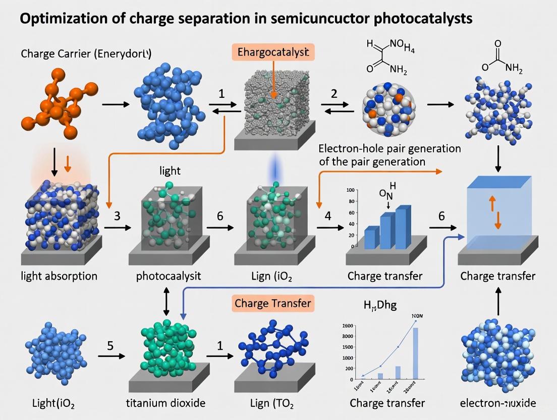
In semiconductor photocatalysis, the absorption of light generates electron-hole pairs. The efficient separation of these photogenerated charges is a critical determinant of overall photocatalytic performance, as it directly influences the number of charge carriers available to drive chemical reactions. Rapid recombination of these charges is a primary factor limiting the efficiency of photocatalytic processes, including hydrogen evolution and nitrogen reduction for ammonia synthesis.
Troubleshooting Common Experimental Problems
FAQ 1: My photocatalyst shows low activity despite high purity materials. What could be the cause?
Low photocatalytic activity often stems from inefficient charge separation. This can be due to:
- Suboptimal Heterojunction Design: The energy band alignment between semiconductor components may not facilitate proper charge transfer. Constructing a Z-scheme heterostructure, as demonstrated in Zn-Ni₂P/g-C₃N₄ systems, can significantly improve charge separation by creating an interfacial electric field (IEF) that directs electron flow [1].
- High Bulk Recombination: Defects within the catalyst bulk can act as recombination centers. Strategies like doping (e.g., Zn doping in Niâ‚‚P) can modify the electronic structure and reduce recombination [1].
- Insufficient Active Sites: Even with successful charge separation, a lack of sites for the desired reaction (e.g., Hâ‚‚ evolution) will limit output. Loading cocatalysts like Niâ‚‚P provides active sites and can further enhance charge separation [1].
FAQ 2: How can I confirm that my material's activity is genuine and not a false positive?
False positives are a significant challenge, especially in reactions like photocatalytic nitrogen reduction where ammonia yields can be low.
- Control for Contaminants: Nitrogenous contaminants from feed gases, the experimental setup, or even the catalysts themselves can lead to false ammonia readings [2]. Implement rigorous purification of gases using acid traps or reduced copper catalysts and clean all equipment meticulously with deionized water [2].
- Conduct Rigorous Control Experiments: Always perform control experiments without light, without catalyst, and with an inert gas like Argon. The use of ¹âµNâ‚‚ isotope labeling is a definitive method to confirm that ammonia originates from dinitrogen reduction rather than contaminants [2].
- Report Original Data: To provide a clear view of potential contaminants, report photocatalyst activity as ammonia concentration versus time and include the unnormalized original data from control experiments [2].
FAQ 3: My photocatalyst deactivates quickly during repeated use. How can I improve its stability?
Deactivation can occur due to photocorrosion, poisoning, or structural changes.
- Identify Deactivation Sources: Common poisons include metal oxides/hydroxides (e.g., from Fe(III) ions in wastewater), polymeric aromatics from air pollutants, or precipitated carbon-containing materials that block active sites and UV light [3].
- Test for Longevity: A single activity measurement is only a snapshot. Probe the longevity of your material under accelerated conditions relevant to its application (e.g., accelerated weathering for outdoor coatings, repeated washing for fabrics) [3]. Some materials may even require an initial "break-in" period to reveal their optimal performance [3].
Quantitative Performance of Charge Separation Strategies
The table below summarizes key strategies for enhancing charge separation and their impact on photocatalytic performance.
Table 1: Strategies for Improving Charge Separation in Photocatalysts
| Strategy | Mechanism | Exemplary Material | Reported Performance |
|---|---|---|---|
| Z-Scheme Heterojunction | Mimics natural photosynthesis; enables spatial separation of electrons and holes while preserving strong redox ability [1]. | Zn-Niâ‚‚P/g-C₃Nâ‚„ | Hydrogen production rate: 1077 μmol gâ»Â¹ hâ»Â¹ under visible light; stability up to 49 hours [1]. |
| Interfacial Electric Field (IEF) | Creates a built-in electric field at the heterojunction interface that drives the directional migration of photogenerated charges, preventing recombination [1]. | Zn-Ni₂P/g-C₃N₄ | IEF directed from Zn-Ni₂P to g-C₃N4, accelerating charge separation [1]. |
| Cocatalyst Loading | Serves as an electron sink and provides active reaction sites, thereby extracting charges from the semiconductor and facilitating surface reactions [1]. | Ni₂P, Pt | Zn-Ni₂P/g-C₃N₄ performance exceeded that of Pt/g-C₃N₄ [1]. |
| Doping Modification | Alters the electronic structure and band gap of the semiconductor, which can create internal trapping sites to reduce bulk electron-hole recombination [1]. | Zn-doped Niâ‚‚P | Zn doping led to an upshift of the p-band state density, favorable for H* adsorption in the HER [1]. |
Essential Experimental Protocols
Protocol 1: Synthesis of a Z-Scheme Heterojunction Photocatalyst
This protocol outlines the synthesis of Zn-Ni₂P/g-C₃N₄, a model system for efficient charge separation [1].
- Synthesis of g-C₃N₄ Precursor: Typically, g-C₃N₄ nanosheets are prepared by the thermal polycondensation of nitrogen-rich precursors like melamine or urea.
- Preparation of NiZn-LDH/g-C₃N₄ Composite:
- Dissolve Zinc acetate (Zn(AC)₂·2H₂O, 0.1 mmol), Nickel chloride (NiCl₂·6H₂O, 0.45 mmol), and Urea (3 mmol) in 60 mL of a methanol-water solution (2:3 volume ratio) [1].
- Add a specific mass of g-C₃N₄ (e.g., 25-100 mg) to the solution and stir for 30 minutes.
- Transfer the solution to a 100 mL Teflon-lined autoclave and hydrothermally treat at 170°C for 17 hours.
- After cooling, collect the precipitate (NiZn/g-C₃N₄) by centrifugation, wash with water and ethanol, and dry at 60°C.
- Phosphidation to Form Zn-Ni₂P/g-C₃N₄:
- Place the obtained NiZn/g-C₃N₄ powder and a red phosphorus source in separate porcelain boats inside a tube furnace, with the phosphorus source positioned upstream.
- Heat under a constant Argon flow to a high temperature (e.g., 500°C) for a set time to convert the precursor into the final Zn-Ni₂P/g-C₃N₄ Z-scheme heterojunction [1].
Protocol 2: Standardized Activity Testing and Validation
Ensuring reliable and reproducible activity data is paramount.
- Photocatalytic Hydrogen Evolution Test:
- Disperse a known mass of photocatalyst (e.g., 50 mg) in an aqueous solution containing a sacrificial electron donor (e.g., methanol or triethanolamine).
- Seal the reaction system and evacuate to remove air.
- Irradiate the suspension with a visible-light source (e.g., a 300 W Xe lamp with a UV-cutoff filter).
- Use gas chromatography (GC) with a thermal conductivity detector (TCD) to quantify the evolved hydrogen gas at regular intervals [1].
- Validation Tests to Mitigate False Positives:
- Gas Purity: Purify feed gases (Nâ‚‚, Ar) by passing them through acid solutions (e.g., 0.05 M Hâ‚‚SOâ‚„) to remove ammonia and through KMnOâ‚„ alkaline solution or a reduced copper catalyst to eliminate NOx contaminants [2].
- System Cleanliness: Rigorously wash all reactor components, glassware, and tubing with fresh deionized water before experiments to remove ambient nitrogenous contaminants [2].
- Control Experiments: Always run dark controls (light off, catalyst present) and negative controls (light on, no catalyst) to establish a baseline. For Nâ‚‚ reduction, an Argon control is essential [2].
Visualization of Mechanisms and Workflows
Diagram 1: Charge Separation in a Z-Scheme Heterojunction
Diagram 2: Experimental Workflow for Photocatalyst Optimization
The Scientist's Toolkit: Research Reagent Solutions
Table 2: Essential Materials for Photocatalytic Charge Separation Studies
| Reagent/Material | Function in Research | Application Notes |
|---|---|---|
| g-C₃N₄ | A popular, metal-free, 2D semiconductor substrate with a suitable bandgap for visible light response. Serves as a base for constructing heterojunctions [1]. | Often synthesized from low-cost precursors like urea or melamine. Its intrinsic charge separation is poor, making it an ideal model for modification [1]. |
| Transition Metal Phosphides (TMPs) | Act as highly effective cocatalysts and heterojunction components. They provide good electrical conductivity, metallic character, and abundant active sites for reactions like the Hydrogen Evolution Reaction (HER) [1]. | Niâ‚‚P and Zn-doped Niâ‚‚P are prominent examples. Their high work function facilitates the formation of an Interfacial Electric Field in heterostructures [1]. |
| Methylene Blue (MB) / Indicator Inks | Used for rapid, qualitative screening of photocatalytic activity, especially for self-cleaning function. The visible color change indicates electron reduction capability [3]. | A non-ISO but rapid test. Useful for initial screening of low-activity samples or for testing the uniformity of a photocatalytic film [3]. |
| 4-Chlorophenol | A model pollutant used in standardized tests (ISO) to quantify the activity of powder photocatalysts for water purification applications [3]. | Measures the degradation kinetics of a stable organic compound, providing a benchmark for oxidative activity. |
| Stearic Acid | A model organic contaminant used in standardized tests (ISO) to evaluate the self-cleaning performance of photocatalytic surfaces [3]. | The decrease in stearic acid layer thickness, measured by IR spectroscopy, correlates with photocatalytic oxidation efficiency. |
| Sm21 maleate | Sm21 maleate, CAS:155058-71-2, MF:C22H28ClNO7, MW:453.9 g/mol | Chemical Reagent |
| XV638 | XV638, CAS:183854-11-7, MF:C41H38N6O5S2, MW:758.9 g/mol | Chemical Reagent |
Frequently Asked Questions (FAQs)
Q1: What is the fundamental difference between bulk and surface recombination, and why does it matter for photocatalytic efficiency?
Bulk recombination occurs when photogenerated electrons and holes recombine inside the photocatalyst material before they can reach the surface to participate in chemical reactions. This process typically happens on a timescale of picoseconds, which is much faster than the hundreds of picoseconds required for charges to travel to the surface. Surface recombination occurs when charges that have successfully reached the surface recombine there instead of engaging in redox reactions. Bulk recombination is particularly detrimental as it represents the majority of charge carrier loss, severely limiting the availability of electrons and holes for catalytic applications such as hydrogen production or pollutant degradation [4].
Q2: What experimental strategies can I use to specifically suppress bulk recombination?
Constructing a Bulk Internal Electric Field (BIEF) is considered one of the most effective strategies. This built-in electric field provides a powerful driving force to mediate bulk charge transfer and separation, accelerating the movement of carriers toward the surface and reducing their chances of recombining internally. BIEF can be enhanced through various material engineering approaches including bulk heteroatom doping, vacancy engineering, ion intercalation, and crystal facet engineering, all of which increase the asymmetry of the crystal structure to strengthen this internal field [4].
Q3: How does creating a heterojunction between two semiconductors help reduce recombination?
Heterojunctions, particularly type-II and Z-scheme architectures, facilitate spatial separation of electrons and holes between different materials. In a direct Z-scheme system, for instance, electrons in the conduction band of one semiconductor combine with holes in the valence band of another at the interface. This selective recombination preserves the most reactive electrons and holes with the strongest redox potentials, thereby simultaneously enhancing charge separation and maintaining high catalytic activity. The formation of an internal electric field at the heterojunction interface further drives this directional charge separation [5] [6].
Q4: My photocatalyst shows good charge separation but poor surface reaction kinetics. What surface modifications can help?
Surface modification with cocatalysts can provide additional active sites and improve surface reaction kinetics. For instance, loading transition metal dichalcogenides like NiS₂ onto g-C₃N₄ creates more active sites for the oxygen reduction reaction. Additionally, covalent organic framework (COF) engineering through molecular-level surface functionalization can optimize electron cloud density distribution at the surface, which improves the separation efficiency of electron-hole pairs that reach the surface and increases the number of active sites per unit volume [7] [8].
Troubleshooting Guides
Problem: Rapid Recombination of Photogenerated Carriers
Symptoms:
- Low quantum efficiency despite good light absorption
- Short charge carrier lifetimes measured by transient absorption spectroscopy
- Weak photoluminescence intensity indicating dominant non-radiative recombination
Diagnosis and Solutions:
| Possible Cause | Diagnostic Tests | Solution Approaches |
|---|---|---|
| Strong bulk recombination | Time-resolved photoluminescence (TRPL), Surface photovoltage (SPV) measurements [4] | Engineer Bulk Internal Electric Field (BIEF) through heteroatom doping or vacancy creation [4] |
| Ineffective charge separation at interface | Electrochemical impedance spectroscopy (EIS), Photocurrent response measurements [6] | Construct type-II heterojunctions or Z-scheme systems for spatial charge separation [5] [6] |
| Poor surface active sites | Adsorption capacity tests, Reactive oxygen species (ROS) detection [6] | Decorate with cocatalysts (e.g., NiSâ‚‚) or create surface defects to provide more reaction sites [7] |
| Weak internal electric field | Kelvin probe force microscopy (KPFM), Band structure calculations [4] | Use ferroelectric/piezoelectric materials or crystallographic orientation control to enhance BIEF [4] |
Problem: Inefficient Solar Energy Conversion
Symptoms:
- Poor performance under visible light despite good UV activity
- Low solar-to-hydrogen efficiency
- Limited photocatalytic activity for target reactions
Diagnosis and Solutions:
| Possible Cause | Diagnostic Tests | Solution Approaches |
|---|---|---|
| Large band gap material | UV-Vis diffuse reflectance spectroscopy (DRS), Tauc plot analysis [9] | Elemental doping or formation of solid solutions to narrow band gap [9] |
| Mismatched band alignment | X-ray photoelectron spectroscopy (XPS), Valence band XPS [5] | Design S-scheme or Z-scheme heterojunctions to optimize redox potential [5] |
| Insufficient visible light absorption | UV-Vis DRS, Optical absorption coefficient calculation [10] | Develop 2D/2D heterostructures with enhanced light harvesting [7] |
Experimental Protocols
Protocol 1: Constructing a 2D/2D Heterojunction with Reverse Barrier Layer
Objective: Create a NiS₂/g-C₃N₄ heterojunction with enhanced charge separation for H₂O₂ production [7].
Materials:
- Urea (precursor for g-C₃N₄)
- Nickel sulfide (NiSâ‚‚) cocatalyst
- Ethanol and deionized water
- Acetic acid (catalyst)
Procedure:
- Synthesize 2D g-C₃N₄: Thermal polymerize urea at 580°C in air, then stir the resulting product in pure water at room temperature for 24 hours and dry [7] [8].
- Prepare 2D NiS₂: Use hydrothermal method at 80°C for 6 hours [7].
- Form heterojunction: Employ electrostatic self-assembly by mixing the oppositely charged 2D CN and 2D NiSâ‚‚ components, leveraging their zeta potential values of approximately -19 mV and 2 mV respectively [7].
- Characterize: Use XRD to confirm structure, FTIR to verify chemical bonding, and XPS to analyze surface composition [7].
Key Parameters:
- The reverse barrier layer creates an internal electric field where the field force and band bending produce forces in the same direction upon photogenerated electron transfer [7].
- This configuration enables electrons on NiS₂ to reduce O₂ to form •O₂⻠radicals, which subsequently generate H₂O₂ [7].
Protocol 2: Quantitative Analysis of Charge Separation Efficiency
Objective: Quantitatively evaluate the effectiveness of charge separation strategies [4].
Materials:
- Photocatalyst samples
- Electrochemical workstation with standard three-electrode cell
- UV-Vis spectrophotometer
- Time-resolved fluorescence spectrometer
Procedure:
- Photoelectrochemical measurements:
Spectroscopic characterization:
Photocatalytic activity assessment:
Data Presentation
Table 1: Performance Comparison of Charge Separation Strategies
| Strategy | Material System | Charge Separation Efficiency Improvement | Quantum Efficiency (%) | Key Mechanism |
|---|---|---|---|---|
| Reverse Barrier Layer | 2D/2D NiS₂/g-C₃N₄ [7] | Significant improvement in electron-hole separation | Not reported | Internal electric field and band bending synergy [7] |
| BIEF Engineering | Doped/Ferroelectric Materials [4] | Enhanced bulk charge separation | Varies by material | Spontaneous polarization-induced internal field [4] |
| Z-Scheme Heterojunction | Bi₂WO₆/ZnIn₂S₄ [6] | Efficient spatial charge separation | Not reported | Directional charge transfer across interface [6] |
| Surface Modification | CN-306 COF [8] | Enhanced electron-hole distribution | 7.27% (at 420 nm) | Optimized electron cloud density redistribution [8] |
| Type-II vdWHs | MoTeâ‚‚/Tlâ‚‚O [10] | Suppressed carrier recombination | ~2% (Power conversion) | Interlayer electric field-driven separation [10] |
Table 2: Characterization Techniques for Recombination Analysis
| Technique | Information Obtained | Applicability | Limitations |
|---|---|---|---|
| Time-Resolved Photoluminescence (TRPL) | Charge carrier lifetime, recombination kinetics [4] | Bulk and surface recombination | Requires specialized equipment |
| Surface Photovoltage (SPV) | Surface charge separation efficiency [4] | Surface and interface recombination | Semi-quantitative |
| Open-Circuit Photovoltage Decay | Charge separation and recombination dynamics [7] | Overall recombination assessment | Indirect measurement |
| Electrochemical Impedance Spectroscopy (EIS) | Charge transfer resistance, interfacial properties [6] | Interface characterization | Complex data interpretation |
| Mott-Schottky Analysis | Band alignment, carrier concentration [5] | Heterojunction characterization | Requires specific conditions |
Visualization
Diagram 1: Charge Separation Pathways in Heterojunctions
Charge Separation Mechanisms
Diagram 2: Experimental Workflow for Recombination Analysis
Recombination Analysis Workflow
The Scientist's Toolkit
Table 3: Essential Research Reagents and Materials
| Material/Reagent | Function | Application Example |
|---|---|---|
| Urea | Precursor for g-C₃N₄ synthesis [7] [8] | Thermal polymerization to create 2D carbon nitride base material [7] |
| Transition Metal Dichalcogenides (NiS₂) | Cocatalyst for active site provision [7] | Creating reverse barrier layer heterojunctions with g-C₃N₄ [7] |
| Terephthalaldehyde | Organic linker for COF formation [8] | Constructing covalent organic frameworks with enhanced charge separation [8] |
| Bismuth Tungstate (Bi₂WO₆) | Bi-based photocatalyst with narrow band gap [6] | Forming Z-scheme heterojunctions with ZnIn₂S₄ [6] |
| Zinc Indium Sulfide (ZnInâ‚‚Sâ‚„) | Ternary metal sulfide photocatalyst [6] | Creating staggered band alignment in heterostructures [6] |
| Ammonium Oxalate | Hole scavenger in photocatalytic reactions [6] | Trapping holes to study electron-driven reduction pathways [6] |
| AZ084 | AZ084|Potent CCR8 Antagonist For Research | AZ084 is a potent, selective, allosteric CCR8 antagonist (Ki=0.9 nM) for cancer and asthma research. This product is For Research Use Only, not for human consumption. |
| 6RK73 | 6RK73, MF:C13H17N5O2S, MW:307.37 g/mol | Chemical Reagent |
Frequently Asked Questions (FAQs)
Q1: What are the fundamental roles of Band Gap Engineering and Internal Electric Fields in photocatalysis? Band gap engineering and internal electric fields (IEFs) are cornerstone principles for optimizing charge separation in semiconductor photocatalysts. Band gap engineering directly controls a material's light absorption capacity by adjusting the energy difference between its valence and conduction bands, ensuring optimal utilization of the solar spectrum. [11] Simultaneously, internally generated electric fields, which can arise from ferroelectric polarization, heterojunction interfaces, or facet junctions, provide a powerful driving force to physically separate photogenerated electrons and holes, thereby drastically reducing their recombination rate. [11] [12] The synergy between a well-designed band structure and a strong IEF is critical for achieving high photocatalytic efficiency. [13]
Q2: How can I consciously design a Z-scheme charge transfer pathway in a heterostructure? Conscious modulation of a Z-scheme pathway relies on two key factors: intimate interfacial contact and a well-defined internal electric field. Research on a ZnInâ‚‚Sâ‚„/MoSeâ‚‚ heterostructure demonstrates that forming atomic-level interfacial chemical bonds (e.g., Mo-S bonds) creates a direct "bridge" for charge transfer. [11] Furthermore, an internal electric field, established due to differences in work function between the two semiconductors, provides the directional driving force that steers electrons from the conduction band of one component to recombine with the holes in the valence band of the other. This preserves the most energetic charges for redox reactions. [11]
Q3: Why does my ferroelectric photocatalyst, which has a strong intrinsic polarization field, show poor activity? A strong bulk polarization field does not guarantee high surface reactivity. In ferroelectric materials like PbTiO₃, surface defects can trap charge carriers and become recombination centers. [12] For instance, Ti vacancy defects near the positively polarized facets of PbTiO₃ were found to trap electrons and promote recombination, severely impeding photocatalytic performance. This indicates that inefficient charge utilization at the surface, rather than a lack of charge separation in the bulk, is often the limiting factor. [12] Mitigating these surface defects is essential for translating efficient bulk separation into surface reactions.
Q4: What are some practical strategies to enhance the Internal Electric Field in a particulate photocatalyst? Several advanced strategies have proven effective:
- Constructing Inter-facet Junctions: Engineering crystals with specific exposed facets (e.g., {010} and {110} facets on BiVOâ‚„) creates a natural potential difference, forming an IEF that drives spatial charge separation. [14]
- Ferroelectric Polarization: Utilizing single-domain ferroelectric materials (e.g., PbTiO₃) provides a permanent, strong built-in electric field for charge separation. [12]
- Building S-Scheme Heterojunctions: Coupling two semiconductors with matched band structures and Fermi levels generates an IEF at their interface, which facilitates the desired Z-scheme-like charge transfer. [15] [11]
- Creating an Electron Transfer Layer (ETL): Modifying a surface with a specific ETL, as demonstrated with NaOH-etched BiVOâ‚„:Mo, can intensify the existing inter-facet IEF by over 10 times, leading to exceptional charge separation efficiency exceeding 90%. [14]
Troubleshooting Guide
| Problem Phenomenon | Possible Root Cause | Diagnostic Experiments | Proposed Solution & Rationale |
|---|---|---|---|
| Low photocatalytic efficiency despite good light absorption. | Severe bulk charge recombination due to insufficient driving force for separation. | Perform surface photovoltage spectroscopy or transient absorption spectroscopy to monitor charge lifetime. [16] | Solution: Introduce a stronger Internal Electric Field via heterojunction or ferroelectric engineering. [17] [12]Rationale: The IEF provides a directional force that actively pulls electrons and holes apart, reducing recombination. |
| Z-scheme heterostructure performs no better than a simple mixture. | Poor interfacial contact leading to inefficient charge transfer between components. | Conduct HRTEM to examine interface intimacy; use XPS to check for interfacial chemical bonds. [11] | Solution: Employ a defect-induced strategy to form atomic-level interfacial chemical bonds (e.g., Mo-S bonds). [11]Rationale: Chemical bonds act as atomic-scale "bridges," enabling rapid Z-scheme charge flux instead of random diffusion. |
| Ferroelectric photocatalyst shows low activity despite a monodomain structure. | Surface defects (e.g., vacancies) acting as charge traps and recombination centers. [12] | Use HR-STEM and Electron Energy Loss Spectroscopy (EELS) to analyze surface atomic structure and defect states. [12] | Solution: Selectively grow a passivation nanolayer (e.g., SrTiO₃ on PbTiO₃) to mitigate surface defects. [12]Rationale: The nanolayer eliminates trapping sites, creating an efficient electron transfer pathway and extending charge lifetime from microseconds to milliseconds. |
| Charge separation is inefficient in a visible-light oxide photocatalyst. | The intrinsic built-in electric field (e.g., from facet junctions) is too weak. | Use Kelvin Probe Force Microscopy (KPFM) to map the surface potential difference between different facets. [14] | Solution: Construct an Electron Transfer Layer (ETL) via surface etching/doping to enlarge the potential difference. [14]Rationale: The ETL intensifies the IEF by over 10 times, creating a cascade that drives exceptionally efficient spatial charge separation (>90%). |
Quantitative Data for Performance Comparison
Table 1: Performance metrics of selected photocatalytic systems employing band gap and IEF engineering.
| Photocatalytic System | Engineering Strategy | Key Performance Metric | Enhancement Factor vs. Baseline | Reference / Source |
|---|---|---|---|---|
| ZnO/MoSâ‚‚ Layered Heterostructure | Solution-phase heterostructure for physical charge separation. | 50% higher efficiency in rhodamine B degradation. | 1.5x vs. individual or physically mixed materials. | [18] |
| Sv-ZnInâ‚‚Sâ‚„/MoSeâ‚‚ Z-Scheme | Interfacial Mo-S bond & IEF modulation. | Hâ‚‚ evolution: 63.21 mmol·gâ»Â¹Â·hâ»Â¹; AQY @420nm: 76.48%. | ~18.8x higher Hâ‚‚ rate vs. pristine ZnInâ‚‚Sâ‚„. | [11] |
| PbTiO₃/SrTiO₃ Core/Shell | Surface defect passivation on a ferroelectric material. | Apparent Quantum Yield for overall water splitting @365nm. | 400x enhancement vs. unmodified PbTiO₃. | [12] |
| BiVOâ‚„:Mo with ETL | Electron Transfer Layer to intensify inter-facet IEF. | Charge separation efficiency @420nm: >90%. | IEF intensity enhanced by ~12x. | [14] |
Detailed Experimental Protocols
Objective: To create a well-defined 2D/2D heterostructure via a straightforward solution-based method for enhanced visible-light photocatalysis.
Key Reagent Solutions:
- Zinc Salt Precursor: e.g., Zinc nitrate hexahydrate (Zn(NO₃)₂·6H₂O).
- Molybdenum Source: Ammonium molybdate tetrahydrate ((NH₄)₆Mo₇O₂₄·4H₂O).
- Sulfur Source: Thiourea (CHâ‚„Nâ‚‚S).
- Reaction Solvent: Deionized water.
Step-by-Step Workflow:
- Dispersion of Template: Begin by dispersing a pre-synthesized few-layer MoSâ‚‚ suspension in deionized water.
- Precursor Addition: Introduce the zinc salt precursor (e.g., Zn(NO₃)₂) into the suspension under constant stirring. The Zn²⺠ions are attracted to and stabilized on the surface of the MoS₂ layers.
- Hydroxide Formation: Slowly add a mild base (e.g., NaOH) to the solution. This induces the formation of a zinc hydroxide intermediate phase that nucleates epitaxially on the MoSâ‚‚ template.
- Hydrothermal Transformation: Transfer the mixture into a Teflon-lined autoclave and subject it to a controlled hydrothermal treatment (e.g., 120-180°C for several hours). This step facilitates the in-situ dehydration and transformation of the zinc hydroxide intermediate into two-dimensional ZnO layers.
- Product Isolation: After the reaction, allow the autoclave to cool naturally. Collect the resulting precipitate by centrifugation, and wash it thoroughly with water and ethanol to remove any ionic residues.
- Final Processing: Dry the final product, a layered ZnO/MoS₂ heterostructure, in an oven at 60-80°C.
Objective: To fabricate a direct Z-scheme Sv-ZnInâ‚‚Sâ‚„/MoSeâ‚‚ photocatalyst by utilizing sulfur vacancies (Sv) as anchoring sites for intimate Mo-S bond formation.
Key Reagent Solutions:
- ZIS Precursors: Zinc chloride (ZnCl₂), Indium chloride (InCl₃), and Thioacetamide (C₂H₅NS).
- Defect-Inducing Agent: Hydrazine Monohydrate (N₂H₄·H₂O) – crucial for creating S-vacancies and coordinatively unsaturated S atoms.
- MoSeâ‚‚ Precursors: Sodium molybdate (Naâ‚‚MoOâ‚„) and Selenium powder (Se).
Step-by-Step Workflow:
- Synthesize Sv-Rich ZnIn₂S₄ (Sv-ZIS): Hydrothermally react Zn, In, and S precursors in the presence of N₂H₄·H₂O. The hydrazine selectively creates S-vacancies, resulting in a flower-like Sv-ZIS microsphere.
- Anchor Molybdenum: Disperse the as-synthesized Sv-ZIS in a solvent. Introduce a molybdenum source (e.g., Naâ‚‚MoOâ‚„). The coordinatively unsaturated S atoms at the vacancy sites will act as atomic anchors for Mo atoms, forming initial Mo-S bonds.
- In-situ Growth of MoSeâ‚‚: Add a Se source to the mixture. Under a second hydrothermal treatment, the pre-anchored Mo reacts with Se to in-situ grow MoSeâ‚‚ nanosheets directly on the Sv-ZIS surface, ensuring an intimate interface with covalent Mo-S bonds.
- Characterize the Interface: Confirm the successful formation of the heterostructure and the Mo-S bonds using HRTEM and X-ray photoelectron spectroscopy (XPS).
- Validate the Z-Scheme Mechanism: Use Surface Photovoltage Spectroscopy (SPS) and DMPO spin-trapping Electron Paramagnetic Resonance (EPR) to provide direct evidence of the Z-scheme charge transfer path.
The Scientist's Toolkit: Essential Research Reagents
Table 2: Key reagents and materials for advanced photocatalyst synthesis and characterization.
| Reagent / Material | Function in Research | Example Application |
|---|---|---|
| Hydrazine Monohydrate (N₂H₄·H₂O) | A defect-inducing agent that creates anion vacancies (e.g., S-vacancies) and generates coordinatively unsaturated atoms for subsequent heterostructure bonding. [11] | Creating S-vacancies in ZnIn₂S₄ to serve as anchors for MoSe₂ growth. [11] |
| Sodium Hydroxide (NaOH) | An etching agent that selectively dissolves surface atoms, enabling the formation of an Electron Transfer Layer (ETL) and incorporation of modifying ions. [14] | Creating a complex defect-based ETL on BiVOâ‚„:Mo to intensify the internal electric field. [14] |
| Strontium Titanate (SrTiO₃) Precursors | A passivation layer material grown epitaxially on ferroelectric surfaces to mitigate charge-trapping surface defects. [12] | Coating PbTiO₃ to eliminate Ti-defect sites, enabling efficient electron transfer to cocatalysts. [12] |
| DMPO (5,5-Dimethyl-1-Pyrroline N-Oxide) | A spin-trapping agent used in Electron Paramagnetic Resonance (EPR) spectroscopy to detect and identify short-lived free radical intermediates generated during photocatalysis. [11] | Experimentally proving the Z-scheme mechanism by directly detecting the reactive radical species generated on specific semiconductor components. [11] |
| NCT02 | NCT02, CAS:790245-61-3, MF:C17H16N2O2S, MW:312.4 g/mol | Chemical Reagent |
| ANI-7 | ANI-7|Aryl Hydrocarbon Receptor Activator | ANI-7 is a potent AhR pathway activator that inhibits cancer cell growth. This product is for research use only (RUO) and not for human use. |
Thermodynamic and Kinetic Barriers in Photo-redox Reactions
Frequently Asked Questions (FAQs)
FAQ 1: Why does my photocatalytic reaction proceed slowly even with a thermodynamically favorable catalyst?
The reaction rate is governed by kinetic barriers, not just thermodynamic feasibility. The highest energy transition state controls the overall rate. In photoredox/nickel dual catalysis, for instance, the slowest step could be single-electron transfer, radical generation, or reductive elimination, depending on your specific substrates and conditions [19]. The measured redox potentials confirm thermodynamic viability, but the kinetics of bimolecular radical processes ultimately determine efficiency [19].
FAQ 2: Why is water removal critical in my photocatalytic system, and what methods are effective?
Water can hydrolyze sensitive intermediates, driving the reaction backward. Effective water removal via azeotropic distillation with a Dean-Stark apparatus is often essential, as molecular sieves or desiccants like Naâ‚‚SOâ‚„ may prove insufficient [20]. Physically removing water shifts equilibrium forward, providing both thermodynamic driving force and kinetic acceleration by preventing intermediate decomposition [20].
FAQ 3: How do I identify whether thermodynamics or kinetics limits my photoreaction efficiency?
Perform a thorough mechanistic investigation. Use cyclic voltammetry to establish thermodynamic feasibility of electron transfers [19]. Then apply kinetic analysis like Stern-Volmer studies or laser flash photolysis to identify rate-limiting steps [19]. For semiconductor photocatalysts, spatially resolve reactive sites using techniques like scanning photoelectrochemical microscopy (SPECM) to distinguish between charge separation kinetics and surface reaction thermodynamics [21].
FAQ 4: What strategies can overcome slow charge separation in semiconductor photocatalysts?
Design heterostructures with built-in interfacial electric fields (IEF). Z-scheme heterojunctions between materials with different work functions create IEFs that direct electron-hole separation [1]. For example, Zn-Ni₂P/g-C₃N₄ composites achieve 5.5-fold higher internal electric fields, dramatically improving charge separation and hydrogen evolution rates [1]. Doping and non-covalent coordination in donor-acceptor structures also create asymmetric electron distribution that facilitates charge separation [22].
Troubleshooting Guides
Problem: Low Quantum Efficiency Despite Strong Light Absorption
Potential Causes and Solutions:
Cause: Rapid electron-hole recombination outpacing surface reactions.
- Solution: Engineer stronger interfacial electric fields via Z-scheme heterojunctions. The built-in electric field directionally separates charges [1].
- Experimental Protocol: Synthesize Zn-Ni₂P/g-C₃N₄ composites through hydrothermal reaction coupled with in-situ phosphating. Confirm IEF strength via work function measurements and DFT calculations [1].
Cause: Mismatch between exciton lifetime and reaction timescale.
- Solution: Select materials where strongly-bound excitons (like A-excitons in MoSâ‚‚) outperform weakly-bound ones. In MoSâ‚‚ monolayers, A-excitons show higher internal quantum efficiency than C-excitons [21].
- Experimental Protocol: Use scanning photoelectrochemical microscopy (SPECM) to spatially map quantum efficiency according to exciton type at different excitation wavelengths [21].
Cause: Poor charge transport to active sites.
- Solution: Optimize material morphology to enhance carrier mobility. In MoSâ‚‚ monolayers, photogenerated electrons can travel >80 microns while holes remain stationary [21].
- Experimental Protocol: Employ aligned-unaligned SPECM measurements to separately track electron and hole transport distances and identify charge transport bottlenecks [21].
Problem: Inconsistent Reaction Rates Across Different Experimental Setups
Potential Causes and Solutions:
Cause: Variations in water contamination affecting sensitive intermediates.
- Solution: Implement standardized azeotropic water removal using Dean-Stark apparatus rather than variable efficiency desiccants [20].
- Experimental Protocol: Fit water removal rate constants (k₆ ≈ 2.33×10â»â´ sâ»Â¹) in kinetic models to ensure >99.9% water removal (dryness <25 ppm) for consistent results [20].
Cause: Unidentified rate-determining steps that change with conditions.
- Solution: Construct comprehensive kinetic models incorporating all potential bottlenecks - chemical steps and physical processes like water removal [20].
- Experimental Protocol: Use previously reported DFT energy landscapes to build kinetic networks, then fit experimental data to identify whether dehydration, nucleophilic coupling, or physical separation processes limit rates under your specific conditions [20].
Problem: Poor Catalyst Stability or Rapid Deactivation
Potential Causes and Solutions:
Cause: Oxidation state instability in transition metal catalysts.
- Solution: Understand the complete oxidation state landscape. Nickel catalysts, for instance, can access Niâ°, Niá´µ, Niᴵᴵ, Niᴵᴵᴵ, and Niᴵⱽ states, each with different stabilities [19].
- Experimental Protocol: Employ EPR spectroscopy to detect paramagnetic intermediates and DFT calculations to map oxidation state stability under reaction conditions [19].
Cause: Spatial separation of oxidation and reduction sites causing charge buildup.
- Solution: Balance oxidation and reduction site distribution. In MoSâ‚‚ monolayers, oxidation occurs primarily at edges/corners while reduction happens across the basal plane [21].
- Experimental Protocol: Use SPECM in substrate generation-tip collection mode to spatially map oxidation (negative ΔI) and reduction (positive ΔI) sites separately, then optimize catalyst design accordingly [21].
Table 1: Performance Metrics for Photocatalytic Systems
| Photocatalytic System | Reaction Type | Key Performance Metric | Value | Reference |
|---|---|---|---|---|
| Zn-Niâ‚‚P/g-C₃Nâ‚„ Z-scheme | Hydrogen Evolution | Production Rate | 1077 μmol gâ»Â¹ hâ»Â¹ | [1] |
| Stability Duration | 49 hours | [1] | ||
| NiO-UPDI donor-acceptor | Ciprofloxacin Degradation | Degradation Rate Constant | 0.553 hâ»Â¹ | [22] |
| MoSâ‚‚ Monolayer | Hydrogen Evolution | Detection Current (SPECM) | ~0.5 pA | [21] |
| Redox-Neutral Catalytic Mitsunobu | Esterification | Rate Constant for Water Removal | 2.33×10â»â´ sâ»Â¹ | [20] |
Table 2: Thermodynamic and Kinetic Parameters for Reaction Analysis
| Parameter Type | Specific Measurement | Application in Photo-redox Reactions | Reference Method |
|---|---|---|---|
| Thermodynamic | Redox Potentials | Feasibility of single-electron transfer | Cyclic Voltammetry [19] |
| Kinetic | Quenching Rate Constants | Bimolecular electron transfer efficiency | Stern-Volmer Analysis [19] |
| Spatial Resolution | Quantum Efficiency Maps | Reactive site activity distribution | SPECM [21] |
| Energy Barriers | Transition State Energies | Rate-determining step identification | DFT Calculations [20] |
| Charge Separation | Internal Electric Field Strength | Electron-hole separation efficiency | Work Function Measurements [1] |
Detailed Experimental Protocols
Protocol 1: SPECM for Spatial Mapping of Photocatalytic Sites
Principle: Scanning photoelectrochemical microscopy (SPECM) enables spatial resolution of reactive sites with ~200 nm resolution and direct quantification of redox reactions under illumination [21].
Procedure:
- Sample Preparation: Grow MoSâ‚‚ monolayers on SiOâ‚‚/Si substrates via chemical vapor deposition [21].
- Characterization: Verify monolayer properties through photoluminescence (PL) and Raman spectroscopy (Δpeak = Eâ‚‚g-Aâ‚g ≈ 19 cmâ»Â¹) [21].
- SPECM Setup: Configure in substrate generation-tip collection mode with ultramicroelectrode (UME) probe [21].
- Photo-oxidation Mapping: Use ferrocene dimethanol mediator, measure ΔI = I({}{\text{T,Light}}) - I({}{\text{T,Dark}}) [21].
- Photoreduction Mapping: Detect Hâ‚‚ evolution from water, map reduction efficiency across surface [21].
- Data Analysis: Identify highest photoactivity regions - typically corners for oxidation, basal plane for reduction in MoSâ‚‚ [21].
Protocol 2: Z-Scheme Heterojunction Construction with Enhanced IEF
Principle: Creating heterostructures between semiconductors with different work functions generates interfacial electric fields that accelerate charge separation [1].
Procedure:
- Synthesis of NiZn-LDH: Hydrothermal treatment of Zn(AC)₂·2H₂O, NiCl₂·6H₂O, and urea in methanol-water solution at 170°C for 17 hours [1].
- Composite Formation: Repeat synthesis with varying g-C₃N4 amounts (25-100 mg) to create NiZn/g-C₃N₄ with different ratios [1].
- Phosphidation: Convert to Zn-Ni₂P/g-C₃N₄ using phosphorous source in tube furnace [1].
- Characterization: Confirm Z-scheme structure, measure work function differences, calculate IEF strength via DFT [1].
- Performance Testing: Evaluate hydrogen evolution under visible light, optimize for maximum production rate [1].
Visualization Diagrams
Diagram 1: Charge Separation in Z-Scheme Heterojunction. The interfacial electric field (IEF) directionally separates photogenerated electrons and holes to different reaction sites.
Diagram 2: Kinetic Barriers in Catalytic Reactions. Multiple transition states (TS1, TS2) represent kinetic bottlenecks, while physical processes like water removal provide thermodynamic driving force.
The Scientist's Toolkit: Research Reagent Solutions
Table 3: Essential Materials for Photo-redox Experiments
| Reagent/Material | Function | Application Example | Key Characteristics |
|---|---|---|---|
| Dean-Stark Apparatus | Azeotropic Water Removal | Redox-neutral Mitsunobu reaction [20] | Critical for >99.9% water removal (24.6 ppm) |
| g-C₃N₄ Nanosheets | 2D Semiconductor Support | Z-scheme heterojunction construction [1] | Suitable band structure (~2.7 eV), high surface area |
| Transition Metal Phosphides (Niâ‚‚P) | Cocatalyst for HER | Hydrogen evolution reactions [1] | Narrow band gap, high work function, metallic character |
| Ferrocene Dimethanol (FcDM) | Redox Mediator for SPECM | Mapping oxidation sites [21] | Single electron outer-sphere mechanism |
| Ultramicroelectrode (UME) | Electrochemical Probe | SPECM measurements [21] | ~200 nm spatial resolution for quantum efficiency mapping |
| Zn-Doped Niâ‚‚P | Enhanced IEF Generation | Donor-acceptor composites [1] | Creates asymmetric electron distribution, strengthens dipoles |
| CD532 | CD532, CAS:1639009-81-6, MF:C26H25F3N8O, MW:522.5 g/mol | Chemical Reagent | Bench Chemicals |
| Cmpda | Cmpda, CAS:380607-77-2, MF:C16H28N2O4S2, MW:376.5 g/mol | Chemical Reagent | Bench Chemicals |
Advanced Material Designs and Heterojunction Strategies for Enhanced Charge Separation
FAQs: Fundamentals and Material Selection
Q1: What are the fundamental differences between Type-II, Z-Scheme, and S-Scheme heterojunctions?
The core difference lies in their charge transfer pathways and the resulting redox capabilities.
- Type-II: Designed for optimal spatial charge separation. Electrons and holes migrate to different semiconductors, reducing their chance to recombine. However, this places the electrons at a lower (less negative) conduction band and the holes at a lower (less positive) valence band, which weakens their redox power [23].
- Z-Scheme: Designed to preserve strong redox power. This system mimics natural photosynthesis, combining the strong reduction potential of one semiconductor with the strong oxidation potential of another. This is achieved by recombining the less useful electrons and holes at the interface, leaving the most energetic charge carriers available for reactions [23] [24].
- S-Scheme: A modern refinement of the direct Z-Scheme. It provides a more detailed mechanistic explanation, emphasizing the role of an internal electric field (IEF), band bending, and Coulomb attraction in driving the selective recombination of less useful charges, thereby preserving the most powerful electrons and holes for catalysis [23] [25].
Table 1: Comparison of Heterojunction Charge Transfer Mechanisms and Outcomes.
| Heterojunction Type | Charge Transfer Pathway | Redox Capability | Key Challenge |
|---|---|---|---|
| Type-II | Electrons and holes move to different semiconductors spatially [23]. | Weakened | Sacrifices redox power for improved charge separation [23]. |
| Traditional Z-Scheme | Uses a liquid/solid mediator to recombine charges [24]. | Strong | Mediators can cause side reactions and light shielding [24]. |
| Direct Z-Scheme | Direct interfacial recombination without a mediator [23] [24]. | Strong | Requires high-quality interfaces; mechanism was debated [23] [24]. |
| S-Scheme | IEF and band bending drive selective charge recombination [23] [25]. | Strongest preserved | Can involve high contact resistance at the interface [23]. |
Q2: How do I choose between a Z-Scheme and an S-Scheme for my photocatalytic application?
The S-Scheme is now widely considered an optimized and mechanistically clarified version of the mediator-free direct Z-Scheme [23] [24]. If your goal is to achieve both superior charge separation and maintain maximum redox potential for demanding reactions like overall water splitting or COâ‚‚ reduction, designing an S-Scheme heterojunction is the recommended strategy. The S-Scheme framework provides clearer design principles, emphasizing the need for an oxidation photocatalyst (OP) with a low Fermi level and small work function, and a reduction photocatalyst (RP) with a high Fermi level and large work function to ensure a powerful internal electric field [23].
Q3: What are van der Waals (vdW) heterostructures and why are they beneficial?
Van der Waals heterostructures are constructed by stacking two-dimensional (2D) semiconductors through weak interlayer vdW forces, instead of requiring direct chemical bonding [24].
Benefits include:
- Overcoming Lattice Mismatch: They allow the combination of any two semiconductors without the stringent requirement of lattice matching, minimizing the formation of crystal defects [24].
- Preserving Intrinsic Properties: The weak vdW interaction helps maintain the original electronic properties of the individual components [24].
- Shortened Charge Migration Path: When built from 2D materials, photogenerated carriers are produced in atomically thin layers, drastically reducing the distance they must travel to reach the surface and participate in reactions [24].
Troubleshooting Common Experimental Challenges
Q4: My heterojunction shows poor photocatalytic activity. What could be the cause?
Poor activity often stems from inefficient charge separation or slow surface reaction kinetics.
- Insufficient Interface Contact: A primary cause is poor intimacy at the heterojunction interface. Without close contact, the internal electric field is weak, and charge carriers cannot efficiently transfer between components [23] [26].
- Solution: Employ in-situ growth methods to tightly anchor one component onto the other. For example, in-situ depositing MnWOâ‚„ nanoparticles onto Mnâ‚€.â‚…Cdâ‚€.â‚…S nanorods created an intimate and robust S-scheme interface [25].
- Rapid Bulk Recombination: Even with a good surface heterojunction, charge carriers may recombine within the bulk of the material before they can reach the surface [25].
- Solution: Engineer the bulk material to enhance charge separation. The creation of zinc blende/wurtzite superlattice interfaces inside Mnâ‚€.â‚…Cdâ‚€.â‚…S nanorods created homogeneous internal electric fields that drove ultrafast bulk charge separation [25].
- Lack of Active Sites: The surface may not have enough catalytic sites for the desired reaction (e.g., Hâ‚‚ evolution or COâ‚‚ reduction).
- Solution: Load cocatalysts like Pt, Ni, or Co₃O₄ onto the semiconductor surface. These act as electron sinks and lower the activation energy for surface reactions [27] [28].
Q5: How can I definitively prove the charge transfer mechanism in my heterojunction?
Verifying an S-scheme or Z-scheme pathway requires multiple complementary techniques to build conclusive evidence.
- In-situ Characterization: Use techniques like in-situ X-ray photoelectron spectroscopy (XPS) under light illumination to observe shifts in core-level energy states, which provides direct evidence of band bending and electron flow driven by the internal electric field [25] [26].
- Radical Trapping Experiments: Conduct experiments to identify reactive species. In a true S-scheme, you should detect radicals generated by the highly positive holes in the OP (e.g., •OH from H₂O oxidation) and radicals generated by the highly negative electrons in the RP (e.g., •O₂⻠from O₂ reduction), confirming the preservation of strong redox potentials [23].
- Theoretical Calculations: Perform Density Functional Theory (DFT) calculations to model the electronic structure, charge density difference, and work functions of the individual components and the heterojunction. This can theoretically predict the formation and direction of the internal electric field [26] [28].
- Ultrafast Spectroscopy: Techniques like transient absorption spectroscopy can track the flow and lifetime of photogenerated charges across the interface on picosecond timescales, directly visualizing the S-scheme charge transfer pathway [25].
Advanced Experimental Protocols
Protocol 1: Constructing a Direct Z-Scheme vdW Heterostructure for Water Splitting
This protocol outlines the synthesis of a non-lattice-matched heterostructure using weak van der Waals interactions.
- Material Selection: Choose two semiconductor materials with staggered band alignment (one with a more negative CB for H₂ evolution, e.g., PtS₂; another with a more positive VB for O₂ evolution, e.g., g-C₃N₄) [24].
- Exfoliation: Prepare single- or few-layer nanosheets of the selected semiconductors using techniques like liquid-phase exfoliation [24].
- Hybridization: Mix the dispersions of the two exfoliated nanomaterials. Use stirring, sonication, or self-assembly driven by electrostatic interactions to stack the layers and form the vdW heterostructure [24].
- Characterization: Confirm the successful formation and structure using:
- High-resolution TEM/HAADF-STEM: To observe the layered morphology and lattice fringes [25].
- Raman Spectroscopy: To detect the characteristic shifts that indicate interlayer coupling [24].
- UV-Vis Diffuse Reflectance Spectroscopy: To analyze the light absorption properties of the heterostructure [24].
Protocol 2: Engineering an S-Scheme Heterojunction with Enhanced Internal Electric Field
This protocol details the creation of a CdS/Co₃O₄ Z-scheme heterojunction with sulfur/oxygen dual vacancies to amplify the IEF [26].
- Create Defects: Synthesize defect-rich precursors. For example, generate sulfur vacancies in CdS (CdS-Sv) and oxygen vacancies in Co₃O₄ (Co₃O₄-Ov) through controlled calcination in inert/reducing atmospheres or chemical reduction methods [26].
- In-situ Growth: Couple the materials to form chemical bonds at the interface. Hydrothermally grow CdS-Sv nanoparticles onto Co₃O₄-Ov nanosheets (or vice-versa). This ensures intimate contact and creates atomic-scale channels for directional charge transfer [26].
- Verify the IEF and Mechanism:
- Use DFT calculations to simulate the charge density difference and plot the charge variation across the interface, which visually demonstrates the electron transfer direction and the formation of the IEF [26].
- Perform Kelvin Probe Force Microscopy (KPFM) to measure the surface potential difference and directly map the built-in electric field at the heterojunction interface [28].
- Conduct in-situ irradiated XPS to monitor the binding energy shifts of key elements (e.g., Cd, W) when the light is turned on, confirming the flow of electrons driven by the IEF [26].
Research Reagent Solutions
Table 2: Essential Materials for Heterojunction Construction and Their Functions.
| Material / Reagent | Function in Heterojunction Research | Example Application |
|---|---|---|
| g-C₃N₄ | A metal-free, stable polymer with a visible-light bandgap; often serves as the reduction photocatalyst (RP) in S-schemes [24] [28]. | PtS₂/g-C₃N₄ vdW heterostructure for water splitting [24]. |
| Mnâ‚€.â‚…Cdâ‚€.â‚…S Solid Solution | A tunable sulfide photocatalyst with excellent visible light absorption; can be engineered with internal superlattices [25]. | S-scheme heterojunction with MnWOâ‚„ for highly efficient Hâ‚‚ evolution [25]. |
| CdS-based Materials | A classic visible-light photocatalyst with a sufficiently negative CB for H₂ evolution; often modified to form heterojunctions [26]. | CdS-Sv/Co₃O₄-Ov Z-scheme for biomass conversion [26]. |
| TiO₂-based Materials | A benchmark UV-active photocatalyst; can be doped or modified to form heterojunctions for enhanced activity [24] [28]. | C,N-TiO₂/g-C₃N₄ direct Z-scheme [24]. |
| Defect Engineering Agents (e.g., NaBHâ‚„) | Chemical reductants used to create anion vacancies (S, O) in metal oxides/sulfides, which can modulate electronic structure and enhance IEF [26] [28]. | Creation of sulfur vacancies in CdS [26]. |
System Workflow and Pathway Diagrams
The following diagram illustrates the synergistic strategy of combining bulk and surface charge separation mechanisms, as demonstrated in a high-performance S-scheme system [25].
The following diagram details the charge transfer pathway in an S-scheme heterojunction, showing how strong redox capabilities are preserved [23] [25].
Within semiconductor photocatalyst research, achieving efficient spatial charge separation remains a fundamental challenge limiting overall energy conversion efficiency. Non-covalent donor-acceptor (D-A) composites present a promising strategy by creating organized molecular interfaces that facilitate directional electron transfer while maintaining structural flexibility. This technical framework examines the NiO-UPDI (urea perylene diimide) composite system, where a p-type semiconductor (NiO) and n-type organic semiconductor (UPDI) form non-covalent interfaces that enhance charge separation through complementary electronic properties.
The fundamental operating principle relies on creating type-II heterojunctions where the conduction and valence band alignment drives electron migration toward UPDI while holes transfer to NiO. This directional charge movement significantly reduces electron-hole recombination, extending carrier lifetime and enhancing photocatalytic activity. Unlike covalently-linked D-A systems requiring complex synthesis, non-covalent approaches like electrostatic self-assembly offer simpler fabrication while maintaining precise control over interfacial charge transfer processes.
Troubleshooting Guides: Experimental Challenges and Solutions
Poor Charge Separation Efficiency
Observed Symptoms: Low photocatalytic hydrogen evolution, high electron-hole recombination, minimal current response in photoelectrochemical measurements.
Material Stability and Degradation Issues
Observed Symptoms: Declining performance over reaction cycles, structural changes observed in TEM, leaching of components.
Frequently Asked Questions (FAQs)
Q1: What is the primary advantage of non-covalent versus covalent D-A composites in the NiO-UPDI system?
Non-covalent approaches, particularly electrostatic self-assembly, offer simpler fabrication under mild conditions while maintaining effective charge separation. The ZnTCPP/C60-EDA system demonstrates this principle, achieving electron transfer through electrostatic interactions without complex covalent synthesis, resulting in hydrogen evolution rates of 113.5 μmol hâ»Â¹ [30]. The flexibility of non-covalent bonding allows for self-repairing interfaces and easier optimization of component ratios.
Q2: How does nitrogen doping enhance NiO performance in these composites?
Nitrogen doping serves multiple functions: it converts NiO from p-type to n-type character, enhances COâ‚‚ adsorption capacity, creates oxygen vacancies that serve as active sites, and significantly improves charge separation efficiency. In photocatalytic COâ‚‚ reduction, N-doped NiO achieves a CO yield of 235 μmol·gâ»Â¹Â·hâ»Â¹, which is 16.8 times higher than pristine p-type NiO [31].
Q3: What characterization techniques are essential for verifying successful non-covalent composite formation?
Key techniques include:
- Zeta potential measurements to confirm electrostatic compatibility between components [30]
- Femtosecond transient absorption (fsTA) spectroscopy to directly observe charge transfer dynamics and excited state lifetimes [29]
- TEM with elemental mapping to verify homogeneous distribution without phase separation [29]
- XPS analysis to identify chemical states and interfacial interactions [31]
- Photoelectrochemical measurements to quantify charge separation efficiency [31]
Q4: Why choose UPDI over other organic semiconductors for this composite system?
UPDI possesses several advantageous properties: a strong built-in electric field that promotes intramolecular charge transfer, high thermal and chemical stability due to covalent urea linkages, appropriate energy level alignment with NiO for efficient electron transfer, and excellent visible light absorption capability [29] [33]. The covalent urea linkages in UPDI prevent disintegration under alkaline conditions that plagues self-assembled PDI systems [33].
Q5: How can I optimize the NiO:UPDI ratio for specific photocatalytic applications?
The optimal ratio depends on the target application:
- For photocatalytic hydrogen evolution, ratios of 1:2 to 1:3 (NiO:UPDI) typically perform best, similar to the ZnTCPP/C60-EDA system [30]
- For COâ‚‚ reduction, higher NiO content (up to 1:1) may be beneficial due to the COâ‚‚ adsorption enhancement from N-doped NiO [31]
- For pollutant degradation, lower UPDI content (3:1 to 2:1) can provide better stability in complex water matrices [33] Systematic screening with 5-7 different ratios is recommended while monitoring both activity and stability.
Experimental Protocols
Synthesis of Nitrogen-Doped NiO via Molten-Salt Method
Principle: The molten-salt environment creates a uniform liquid medium that facilitates homogeneous nitrogen incorporation into the NiO lattice, converting it from p-type to n-type character with enhanced conductivity and COâ‚‚ adsorption capability [31].
Step-by-Step Procedure:
- Precursor Preparation: Combine 2g Ni(NO₃)₂·6H₂O with 0.3g urea (nitrogen source) and 10g KCl (molten salt medium) in an agate mortar. Grind for 20 minutes until homogeneous mixture is achieved.
- Thermal Treatment: Transfer mixture to alumina crucible and heat in muffle furnace at 400°C for 2 hours with heating rate of 5°C/min.
- Washing: Cool naturally to room temperature, then disperse resulting powder in deionized water. Centrifuge at 8000 rpm for 5 minutes. Repeat washing cycle 3 times to remove residual salts.
- Drying: Dry washed precipitate at 80°C for 12 hours in vacuum oven.
- Annealing: Calcine final product at 350°C for 1 hour in air to crystallize.
Critical Parameters:
- Urea:Ni ratio controls nitrogen doping level (optimize between 1:4 to 1:8)
- Heating rate ≤5°C/min ensures uniform thermal decomposition
- Final annealing temperature critical for crystallinity without nitrogen loss
UPDI Synthesis and Composite Formation
Principle: Urea-functionalized perylene diimide forms covalently-linked polymers with enhanced stability compared to self-assembled PDI, maintaining strong built-in electric fields for charge separation while resisting disintegration under alkaline conditions [29] [33].
Step-by-Step Procedure:
- UPDI Synthesis:
- Combine 500mg 3,4,9,10-perylenetetracarboxylic dianhydride (PTCDA) with 5g urea and 50mg Zn(OAc)â‚‚ catalyst
- Heat at 180°C for 4 hours under nitrogen atmosphere with continuous stirring
- Cool to room temperature, crush resulting solid, and wash with hot water to remove excess urea
- Dry at 100°C overnight to obtain crystalline UPDI
- Composite Formation:
- Prepare separate dispersions of 100mg N-NiO in 50mL ethanol and 200mg UPDI in 50mL acetone
- Sonicate both dispersions for 30 minutes to achieve complete dispersion
- Slowly add N-NiO suspension to UPDI suspension dropwise over 20 minutes with vigorous stirring
- Continue stirring for 6 hours at room temperature to facilitate electrostatic self-assembly
- Collect composite by centrifugation at 9000 rpm for 10 minutes
- Dry under vacuum at 80°C for 12 hours
Quality Control Check:
- Verify composite formation by zeta potential measurement (should show intermediate value between components)
- Check homogeneity by TEM with elemental mapping
- Confirm interfacial interaction by FTIR peak shifts
Photocatalytic Hydrogen Evolution Test Protocol
Principle: Under visible light irradiation, the NiO-UPDI composite should exhibit enhanced hydrogen evolution compared to individual components due to improved charge separation at the donor-acceptor interface [30].
Standard Procedure:
- Reaction Setup:
- Disperse 20mg NiO-UPDI composite in 100mL aqueous solution containing 10 vol% triethanolamine as sacrificial electron donor
- Load 1 wt% Pt cocatalyst via in-situ photodeposition using H₂PtCl₆
- Seal system and purge with Nâ‚‚ for 30 minutes to remove dissolved oxygen
Photocatalytic Reaction:
- Illuminate with 300W Xe lamp equipped with 420nm cutoff filter
- Maintain reaction temperature at 25°C using water cooling jacket
- Continuously stir at 300 rpm to maintain suspension
Gas Analysis:
- Collect 0.5mL gas sample from headspace at 1-hour intervals
- Analyze Hâ‚‚ content using gas chromatography with TCD detector
- Calculate evolution rate using calibration curve from standard Hâ‚‚ mixtures
Expected Performance Metrics:
- Reference system: ZnTCPP/C60-EDA achieves 113.5 μmol hâ»Â¹ Hâ‚‚ evolution [30]
- Quality composite should achieve at least 2x activity of physical mixture
- Linear production over 5 hours indicates stability
Quantitative Performance Data
Visualization of Mechanisms and Workflows
Charge Separation Mechanism in NiO-UPDI Composites
Experimental Workflow for Composite Synthesis
Research Reagent Solutions
Frequently Asked Questions (FAQs) and Troubleshooting
FAQ 1: What are the primary reasons for modifying g-C3N4 with non-metal elements like Boron (B), Phosphorus (P), and Sulfur (S)?
Modifying g-C3N4 with non-metal elements is a key strategy to overcome its inherent limitations as a photocatalyst, specifically to enhance charge separation, which is the core focus of this thesis. Pristine g-C3N4 suffers from rapid recombination of photogenerated electron-hole pairs, which wastes solar energy and limits its catalytic efficiency [34] [35]. Non-metal doping directly addresses this by:
- Altering the Electronic Band Structure: Doping can reduce the bandgap of g-C3N4, extending its light absorption into the visible region and creating more photogenerated charges [34] [36]. For instance, carbon self-doping can activate n→π* electronic transitions, significantly redshifting light absorption [36].
- Promoting Charge Separation: Dopant atoms introduce defects that can trap charge carriers, slowing down their recombination and prolonging their lifetime. This enhances the availability of electrons and holes for surface reactions like CO2 reduction or H2 production [34] [37].
- Improving Electrical Conductivity: Elements like sulfur can enhance electron transfer across the π-conjugated framework, facilitating the movement of charges to the catalyst surface [34] [36].
FAQ 2: During synthesis, my doped g-C3N4 sample shows lower photocatalytic activity than the pristine material. What could be the cause?
This is a common issue often traced to suboptimal synthesis parameters. The primary factors to investigate are:
- Dopant Concentration: Excessive doping can create recombination centers that trap electrons and holes, causing them to recombine instead of separating. This defeats the purpose of modification [35]. It is crucial to systematically optimize the precursor ratios.
- Polymerization Temperature and Time: The crystallinity and degree of condensation of g-C3N4 are highly sensitive to the calcination conditions [38]. Incomplete polymerization at low temperatures yields materials with many uncondensed amino groups, which act as recombination sites. Conversely, excessively high temperatures can degrade the structure. For melamine-based precursors, a temperature of around 520-550°C is often effective [38].
- Precursor Homogeneity: For doping methods involving a mixture of precursors (e.g., urea and thiourea), ensure a homogeneous mixture before calcination. Inhomogeneous mixing can lead to uneven doping and poorly defined material properties [39].
FAQ 3: How can I experimentally confirm that non-metal doping has successfully improved charge separation in my g-C3N4 samples?
You can verify enhanced charge separation through a combination of spectroscopic and photoelectrochemical characterizations:
- Photoluminescence (PL) Spectroscopy: A significant decrease in PL intensity for the doped sample compared to pristine g-C3N4 strongly indicates suppressed electron-hole recombination [35] [38].
- Time-Resolved Photoluminescence (TRPL): This technique measures the lifetime of photogenerated charges. A prolonged average lifetime in doped samples is direct evidence of more efficient charge separation [35].
- Photoelectrochemical Tests: Transient photocurrent response and Electrochemical Impedance Spectroscopy (EIS) are highly effective. Enhanced photocurrent and a smaller arc radius in the EIS Nyquist plot for the doped sample signify improved charge separation and transfer efficiency [36] [35].
- UV-Vis Diffuse Reflectance Spectroscopy (DRS): This confirms the successful modulation of the optical properties, such as a redshift in the absorption edge, indicating a narrowed bandgap [34] [38].
Quantitative Performance Data of Non-Metal Doped g-C3N4
The following table summarizes the enhanced photocatalytic performance of non-metal doped g-C3N4 for various reactions, as reported in recent literature. The data clearly demonstrates the efficacy of doping in improving activity.
Table 1: Photocatalytic Performance of Non-Metal Doped g-C3N4.
| Dopant Element | Precursor(s) Used | Photocatalytic Reaction | Performance Metric | Reported Enhancement Over Pristine g-C3N4 | Reference |
|---|---|---|---|---|---|
| Sulfur (S) | Thiourea | COâ‚‚ Reduction to CHâ‚„ | CHâ‚„ Production Rate | 7.87 nmol/(mL·gâ‚‘â‚ₜ·h) | [34] |
| Oxygen (O) | Hydrogen Peroxide / Melamine | CO₂ Reduction to CH₃OH | CH₃OH Production Rate | 5-fold increase (0.88 vs. 0.17 μmol/g/h) | [34] |
| Carbon (C) & N-Defects | Urea & Uric Acid | Hâ‚‚ Evolution | Hâ‚‚ Production Rate | Significant enhancement (Specific rate not provided) | [36] |
| Sulfur (S) | Melamine & Thiourea | Dye Degradation (Methylene Blue) | Sonophotocatalytic Degradation Efficiency | 4 times faster than photocatalysis alone | [38] |
Detailed Experimental Protocols
Protocol 1: Synthesis of S-Doped g-C3N4 for Enhanced CO2 Reduction
This protocol is adapted from research focused on improving electron transfer for photocatalytic applications [34].
Research Reagent Solutions:
- Thiourea (≥99%): Serves as the single source for both carbon nitride and sulfur dopant.
- Ethanol (96%): Used for washing the synthesized polymer to remove unreacted species.
Step-by-Step Methodology:
- Precursor Preparation: Place 10 g of thiourea in a covered alumina crucible.
- Thermal Polycondensation: Heat the crucible in a muffle furnace to 600 °C at a ramp rate of approximately 10 °C per minute. Maintain this temperature for 2 hours.
- Product Recovery: After the furnace cools to room temperature naturally, collect the resulting solid. This is the bulk S-doped g-C3N4.
- Post-Synthesis Treatment: Wash the solid multiple times with ethanol and double-distilled water to remove any unreacted precursors or by-products.
- Drying: Dry the final product in an oven at 60 °C for 12 hours to obtain the S-doped g-C3N4 as a yellow powder.
Protocol 2: Synthesis of Carbon Self-Doped and Nitrogen-Defective g-C3N4 Nanosheets
This advanced protocol creates a dual-modified material with synergistic effects for superior charge separation [36].
Research Reagent Solutions:
- Urea: Primary precursor for g-C3N4.
- Uric Acid: Source of carbon for self-doping.
- Deionized Water: Solvent for the self-assembly process.
Step-by-Step Methodology:
- Supramolecular Pre-assembly: Dissolve 20 g of urea and 200 mg of uric acid in 30 mL of deionized water. Sonicate the mixture at 60 °C for 1 hour to ensure a homogeneous dispersion.
- Solvent Evaporation: Transfer the solution to an oil bath and stir at 120 °C for 3 hours to completely evaporate the solvent, forming a supramolecular urea-uric acid complex.
- Initial Polymerization: Place the dried complex in a covered crucible and heat at 550 °C for 2 hours in a muffle furnace. The resulting powder is the carbon self-doped g-C3N4 (denoted CNuu-550).
- Thermal Exfoliation (Introducing N-Defects): Further heat a portion of the CNuu-550 powder at 640 °C for 30 minutes. This step simultaneously exfoliates the bulk material into ultrathin nanosheets and introduces nitrogen defects, creating the final optimized photocatalyst (CNuu-640).
Research Reagent Solutions
The following table lists key reagents and their specific functions in the synthesis and modification of g-C3N4 photocatalysts.
Table 2: Essential Reagents for Non-Metal Doping of g-C3N4.
| Reagent | Function in Doping and Modification | Key Consideration |
|---|---|---|
| Urea | A common, low-cost nitrogen-rich precursor for synthesizing pristine g-C3N4. Also used in mixtures for co-doping [34] [39]. | Pyrolysis releases gases that create a porous structure, which can enhance surface area [34]. |
| Thiourea | Primary precursor for introducing Sulfur (S) dopant atoms into the g-C3N4 matrix during thermal polymerization [34] [38]. | The S atoms typically substitute corner-site N atoms, modulating the electronic structure and improving electron transfer [34]. |
| Boric Acid | A common precursor for introducing Boron (B) dopant atoms into the g-C3N4 framework [34]. | Boron doping is reported to alter the band gap position and widen photon absorption, boosting charge transfer efficiency [34]. |
| Ammonium Dihydrogen Phosphate | A precursor used for incorporating Phosphorus (P) into g-C3N4 [34]. | The addition of red phosphorus to g-C3N4 has been shown to substantially enhance charge carrier separation [34]. |
| Uric Acid | Used as a carbon source for carbon self-doping. It enables supramolecular pre-assembly with urea, leading to an extended π-conjugated system [36]. | This impurity-free modification enhances light absorption and creates conductive interlayer networks for better charge mobility [36]. |
| Melamine | A standard precursor for producing g-C3N4 with higher crystallinity compared to urea [38]. | Higher calcination temperatures (e.g., >500°C) are often used with melamine to achieve improved crystallinity and a suitable band gap [38]. |
Cocatalyst Loading for Selective Charge Extraction and Reaction Acceleration
Frequently Asked Questions (FAQs)
FAQ 1: What is the fundamental role of a cocatalyst in semiconductor photocatalysis?
Cocatalysts are substances added in small quantities to a catalyst to improve its activity, selectivity, or stability [40]. In semiconductor photocatalysis, their primary roles are multifold:
- Promoting Charge Separation: They provide trapping sites for photogenerated electrons and/or holes, facilitating their separation and mitigating recombination [40] [41].
- Accelerating Surface Reaction Kinetics: Cocatalysts offer active sites with refined electronic structures that lower the activation energy for surface redox reactions, such as hydrogen evolution (HER) and oxygen evolution (OER) [40] [42].
- Suppressing Photocorrosion: By timely consumption of photogenerated charges, particularly holes, cocatalysts can protect the underlying semiconductor photocatalyst from oxidative degradation [40] [42].
FAQ 2: Why is dual-cocatalyst loading often more effective than single-cocatalyst loading?
Loading dual cocatalysts, one for reduction (e.g., for H₂ evolution) and one for oxidation (e.g., for O₂ evolution), can significantly enhance activity for overall water splitting [41]. This strategy effectively separates the reduction and oxidation active sites, which not only accelerates the respective half-reactions but also suppresses the reverse reaction of H₂ and O₂ recombining into water [42]. For instance, a system using Rh/Cr₂O₃ as a reduction cocatalyst and Co₃O₄ as an oxidation cocatalyst achieved a high solar-to-chemical conversion efficiency [40].
FAQ 3: My photocatalyst shows good charge separation but low overall activity. What could be the issue?
This often indicates a bottleneck in the surface reaction kinetics. While charge separation is necessary, the photogenerated carriers must be efficiently utilized in the redox reactions. This issue can be addressed by:
- Ensuring Cocatalyst Suitability: Verify that the loaded cocatalyst has appropriate energy band alignment with the semiconductor to extract the specific charge carrier (electron or hole) required for your target reaction [40].
- Optimizing Cocatalyst Dispersion and Loading: The cocatalyst should be highly dispersed to provide a maximum number of active sites. However, excessive loading can block light absorption by the semiconductor and/or act as charge recombination centers [42].
FAQ 4: How can I determine if my cocatalyst is effectively extracting electrons or holes?
The charge transfer pathway is governed by the energy band alignment at the semiconductor-cocatalyst interface [40].
- For electron-extracting cocatalysts (e.g., Pt, Ni), the Fermi level of the metal should be lower than the conduction band of the semiconductor to form a Schottky junction that promotes electron transfer from the semiconductor to the cocatalyst [40].
- For hole-extracting cocatalysts (e.g., IrO₂, Co₃O₄), an Ohmic junction or a staggered band alignment that favors hole migration from the semiconductor valence band to the cocatalyst is required [40]. Advanced characterization techniques like in-situ electron spin resonance (ESR) can directly track the flow of holes to molecular cocatalysts [43].
Troubleshooting Guide
Problem 1: Rapid Deactivation of Photocatalyst During Reaction
- Potential Cause: Photocorrosion, where the semiconductor itself is oxidized by the accumulated photogenerated holes.
- Solution:
- Load a suitable oxidation cocatalyst (e.g., IrOâ‚‚, RuOâ‚‚, CoOx) to rapidly consume holes [42] [41].
- For H₂ evolution cocatalysts like Pt, consider embedding them within a protective shell (e.g., Cr₂O₃) to prevent contact with oxygen and suppress the reverse reaction, thereby enhancing stability [42].
Problem 2: Low Quantum Efficiency Despite High Light Absorption
- Potential Cause: Severe bulk or surface recombination of photogenerated electron-hole pairs.
- Solution:
- Load Dual Cocatalysts: Implement separate reduction and oxidation cocatalysts to simultaneously extract electrons and holes, preventing their recombination [41].
- Optimize Interface Engineering: Employ a loading method that ensures an intimate interface (e.g., in-situ photodeposition or impregnation) between the cocatalyst and semiconductor to minimize interfacial charge transfer resistance [40] [42].
- Consider Homogeneous Cocatalysts: In some cases, molecular co-catalysts like trifluoroacetic acid (TFA) can act as efficient hole shuttles, maximizing contact areas with reactants and significantly boosting Hâ‚‚ evolution [43].
Problem 3: Inconsistent Cocatalyst Deposition and Poor Dispersion
- Potential Cause: Uncontrolled loading process leading to large, agglomerated cocatalyst particles.
- Solution:
- Switch Loading Methods: If impregnation leads to poor dispersion, try photodeposition, which can selectively deposit metals onto specific sites using light-induced redox reactions [42].
- Control Synthesis Parameters: Precisely adjust precursor concentration, pH, temperature, and lighting conditions during deposition to control nucleation and growth rates for a uniform, nano-sized cocatalyst distribution [42].
Quantitative Performance Data
The following table summarizes performance data for various cocatalyst-modified photocatalytic systems from the literature.
Table 1: Performance Comparison of Selected Cocatalyst-Modified Photocatalytic Systems
| Photocatalyst | Cocatalyst(s) | Reaction | Performance Metric | Reported Value | Reference |
|---|---|---|---|---|---|
| Kâ‚„Nb₆Oâ‚₇ Nanosheets | Trifluoroacetic Acid (TFA) | Hâ‚‚ Evolution | Hâ‚‚ Evolution Rate | 6,344 μmol gâ»Â¹ hâ»Â¹ | [43] |
| Kâ‚„Nb₆Oâ‚₇ Nanosheets | None (Blank) | Hâ‚‚ Evolution | Hâ‚‚ Evolution Rate | ~195 μmol gâ»Â¹ hâ»Â¹ | [43] |
| (Gaâ‚â‚‹â‚“Znâ‚“)(Nâ‚â‚‹â‚“Oâ‚“) | RhCrOâ‚“ | Overall Water Splitting | Apparent Quantum Yield (AQY) @ 420-440 nm | 2.5% | [42] |
| InGaN/GaN NWs | Rh/Cr₂O₃ & Co₃O₄ | Overall Water Splitting | Solar-to-Chemical Conversion Efficiency | 9.2% | [40] |
Experimental Protocols
Protocol 1: Impregnation-Calcination Method for Loading Metal Oxide Cocatalysts
This is a common method for loading cocatalysts such as RhCrOâ‚“ [42].
- Impregnation: Disperse the pristine semiconductor photocatalyst powder (e.g., 1.0 g) in an aqueous solution (e.g., 50 mL) containing the desired metal precursors (e.g., Na₃RhCl₆·2H₂O and Cr(NO₃)₃·9H₂O).
- Drying: Stir the suspension vigorously while slowly evaporating the solvent (e.g., using a rotary evaporator or water bath) to ensure uniform precipitation of the precursor onto the photocatalyst surface.
- Calcination: Collect the dried powder and calcine it in a furnace under a controlled atmosphere (e.g., air or nitrogen) and temperature (typically 300-500°C) for 1-4 hours. This step pyrolyzes the precursors into the active cocatalyst nanoparticles (e.g., RhCrOₓ).
- Post-treatment: The resulting powder may be washed and dried before photocatalytic testing.
Protocol 2: In-situ Photodeposition for Loading Metal Cocatalysts
This method is widely used for loading noble metals like Pt [42].
- Reaction Mixture Preparation: Prepare an aqueous suspension containing the semiconductor photocatalyst, a sacrificial reagent (e.g., methanol for H₂ evolution cocatalysts), and the metal salt precursor (e.g., H₂PtCl₆).
- Illumination: Stir the suspension under light irradiation (e.g., a Xe lamp). Photogenerated electrons will reduce the metal cations (Ptâ´âº) to their metallic form (Ptâ°), depositing them onto the semiconductor surface.
- Separation and Washing: After the reaction, centrifuge the suspension to collect the photocatalyst powder loaded with the metal cocatalyst. Wash thoroughly with deionized water to remove residual ions and dry in an oven.
Cocatalyst Charge Transfer Mechanisms
The diagram below illustrates the primary charge transfer mechanisms at semiconductor-cocatalyst interfaces.
Photodeposition Experimental Workflow
The following flowchart outlines the key steps for loading a cocatalyst via the photodeposition method.
Research Reagent Solutions
Table 2: Essential Materials for Cocatalyst Loading and Testing
| Reagent/Material | Function/Application | Key Considerations |
|---|---|---|
| Na₃RhCl₆·2H₂O | Rhodium precursor for impregnation of H₂ evolution cocatalysts (e.g., RhCrOₓ) [42]. | High purity ensures reproducible cocatalyst composition and performance. |
| H₂PtCl₆·6H₂O | A common platinum precursor for photodeposition of metallic Pt nanoparticles as reduction cocatalysts [42]. | Concentration controls the particle size and loading amount of Pt. |
| Cr(NO₃)₃·9H₂O | Chromium precursor used to form a Cr₂O₃ shell around metal NPs to suppress H₂-O₂ reverse reaction [42]. | |
| Trifluoroacetic Acid (TFA) | A molecular co-catalyst that acts as a homogeneous hole shuttle, drastically increasing Hâ‚‚ evolution rates [43]. | Forms a reversible redox couple (TFA•/TFAâ»). Requires a sacrificial electron donor (e.g., methanol). |
| Methanol | A common sacrificial reagent that irreversibly consumes holes, allowing isolation and study of reduction (Hâ‚‚ evolution) reactions [43]. | Purity is critical to avoid introducing unintended catalytic sites or poisons. |
Frequently Asked Questions (FAQs)
FAQ 1: What are the key strategies to improve charge separation in photocatalysts for pharmaceutical degradation? Improving charge separation is fundamental to enhancing photocatalytic efficiency. Key strategies include:
- Heterojunction Formation: Creating composite materials (e.g., Cu2O/TiO2) to form a junction that facilitates the spatial separation of electrons and holes, inhibiting their recombination [44].
- Cocatalyst Loading: Using materials that act as electron sinks or reaction sites, thereby extracting photogenerated charges from the semiconductor [45].
- Donor-Acceptor Systems: Utilizing organic systems, such as bulk-heterojunctions in organic photovoltaics, which form an interpenetrating network to increase the contact area and facilitate exciton diffusion and charge transfer [46].
- Z-Scheme Mechanisms: Designing nanocomposites that mimic natural photosynthesis, creating a direct Z-scheme for optimal redox reactions, as demonstrated in Cu2O/TiO2 for CO2 reduction [44].
FAQ 2: Which characterization techniques are crucial for diagnosing charge carrier dynamics? Advanced characterization is vital for troubleshooting low activity. Essential techniques include:
- Photoluminescence (PL) Spectroscopy: Directly probes the recombination rate of photogenerated electron-hole pairs; a high PL intensity often indicates high charge recombination [45] [46].
- Transient Absorption Spectroscopy: Measures the time scales of electron transfer and charge carrier lifetimes [45] [44].
- Electron Paramagnetic Resonance (EPR): Identifies radical species generated during photocatalysis, confirming the activity of charge carriers [45].
- Kelvin Probe Force Microscopy (KPFM): Maps surface potentials and visualizes charge separation at the nanoscale [45].
FAQ 3: Why is photocatalyst stability a challenge, and how can it be improved? Photocatalyst deactivation, or poisoning, can occur due to surface fouling by reaction intermediates or material corrosion [47]. Strategies to enhance stability include:
- Immobilization on Supports: Loading the active photocatalytic material on stable, porous supports like coconut shell carbon (CSC) protects it from the aqueous environment and facilitates reuse [46].
- Creating Core-Shell Structures: Coating a less stable material (e.g., Cu2O) with a protective layer (e.g., TiO2) can prevent photocorrosion [44].
- Designing Magnetically Separable Catalysts: Incorporating magnetic components (e.g., CuFe2O4) allows for easy retrieval using an external magnet, improving reusability and reducing physical loss [48].
FAQ 4: How do I identify the main reactive species in my photocatalytic system? Scavenger tests are the standard experimental method. By adding specific chemicals that quench particular reactive species, you can observe the change in degradation efficiency [49] [46].
- Isopropyl Alcohol (IPA): Scavenges hydroxyl radicals (•OH).
- 1,4-Benzoquinone (BQ): Scavenges superoxide anions (O2•â»).
- Triethanolamine or EDTA-2Na: Scavenges photogenerated holes (hâº). A significant drop in the degradation rate upon adding a specific scavenger indicates that the corresponding species plays a dominant role [49].
Troubleshooting Guide
| Problem Symptom | Potential Root Cause | Diagnostic Steps | Coping Strategy |
|---|---|---|---|
| Low degradation efficiency | Rapid electron-hole recombination [47] | Perform PL spectroscopy; if intensity is high, recombination is likely [46]. | Implement a heterojunction structure (e.g., TiO2/ZnO) or cocatalyst (e.g., Au nanoparticles) [45] [50]. |
| Insufficient light absorption [47] | Collect UV-Vis DRS spectra. Check if absorption range matches your light source. | Use a composite with a smaller bandgap or a ternary system (e.g., PM6:Y6:ITCPTC) for broad absorption [46]. | |
| Poor photocatalyst reusability | Photocorrosion or dissolution [44] | Use AAS to measure metal ion leaching in the solution post-reaction [48]. | Stabilize the catalyst on a support (CSC) or use a protective shell (TiO2 on Cu2O) [46] [44]. |
| Loss of catalyst during recovery | Visually inspect for turbidity after separation. | Design a magnetically separable catalyst (e.g., CuFe2O4) for easy retrieval [48]. | |
| Incomplete mineralization | Accumulation of stable intermediate by-products [49] | Use HPLC-MS or LC-QTOF to identify intermediate products [49]. | Optimize reaction time or employ a process coupling with other AOPs to enhance oxidation power [47]. |
| Variable performance with pH | pH-sensitive surface charge & reactivity [48] | Conduct degradation experiments across a pH range (e.g., 3, 7, 11) [48]. | Determine and maintain the optimal pH for your specific catalyst and pharmaceutical target. |
Table 1: Performance metrics of selected photocatalysts for ciprofloxacin (CIP) degradation.
| Photocatalyst | Optimal Loading | Initial CIP Conc. | Light Source | Time (min) | Removal % | Key Kinetic Constant | Citation |
|---|---|---|---|---|---|---|---|
| CuFe2O4@Methyl Cellulose | 0.2 g/50 mL (suspension) | 3 mg/L | Not Specified | 90 | 80.7% (synthetic) | Fitted to Pseudo-first-order | [48] |
| CSC-PM6:Y6:ITCPTC | 0.1 g/50 mL (suspension) | 10 mg/L | Xe lamp (300-1100 nm) | 30 (dark) + 30 (light) | ~99% | Not Specified | [46] |
| g-C3N4 Nanosheets | 0.5 g/L (suspension) | Not Specified | White LEDs (4 x 10 W) | Not Specified | Not Specified | k = 0.035 minâ»Â¹ (Pseudo-first-order) | [49] |
Table 2: Performance of g-C3N4 for various inherent pharmaceuticals in hospital wastewater (300 mg/L catalyst, 4h solar irradiation) [51].
| Pharmaceutical | Initial Concentration (ng Lâ»Â¹) | Removal Percentage (%) |
|---|---|---|
| Amisulpride | Not Specified | 96% |
| O-Desmethyl Venlafaxine | 2924.53 | 83% |
| Venlafaxine | Not Specified | 85% |
| Carbamazepine | Not Specified | 81% |
| Mirtazapine | Not Specified | 34% |
Detailed Experimental Protocols
Protocol 1: Photocatalytic Degradation of Ciprofloxacin using a Magnetic Nanobiocomposite This protocol is adapted from the synthesis and use of CuFe2O4@Methyl Cellulose [48].
Research Reagent Solutions:
- FeCl₃·6H₂O & CuCl₂·2H₂O: Metal precursors for spinel ferrite synthesis.
- Methyl Cellulose (MC): A biopolymer template for green synthesis and composite formation.
- NaOH Solution: Precipitating agent.
- Ciprofloxacin (CIP) Stock Solution: Primary contaminant target.
Synthesis of CuFe2O4@MC:
- Dissolve FeCl₃·6H₂O (20 mmol, 5.4 g) and CuCl₂·2H₂O (10 mmol, 1.7 g) in 50 mL deionized water.
- Add 1 g of methyl cellulose to the solution and stir at room temperature (25 °C).
- Slowly add sodium hydroxide solution to the suspension over 1 hour.
- Transfer the dark brown solution to a microwave oven and heat in intervals (3 × 5 min at 450 W).
- Separate the resulting lightweight sediment powder using an external magnet.
- Wash the product several times with deionized water and dry in a vacuum oven at 100 °C for 24 h.
Photocatalytic Testing:
- Prepare a CIP solution (e.g., 3-9 mg/L) and adjust the pH (e.g., 3, 7, 11) as required.
- Add a specific loading of photocatalyst (e.g., 0.025 - 0.4 g) to the CIP solution.
- Stir the mixture in the dark for 30-60 minutes to establish adsorption-desorption equilibrium.
- Illuminate the solution under your chosen light source while maintaining stirring.
- Collect samples at regular time intervals (e.g., every 15 min).
- Separate the catalyst from the sample (via filtration or magnet) and analyze the supernatant for CIP concentration using High-Performance Liquid Chromatography (HPLC).
Protocol 2: Probing Reactive Species via Scavenger Tests This methodology is critical for diagnosing the degradation mechanism and troubleshooting low activity [49] [46].
Research Reagent Solutions:
- Triethanolamine or EDTA-2Na: Hole (hâº) scavenger.
- 1,4-Benzoquinone (BQ): Superoxide anion (O₂•â») scavenger.
- Isopropyl Alcohol (IPA): Hydroxyl radical (•OH) scavenger.
Experimental Workflow:
- Set up multiple identical photocatalytic reactions with the optimal parameters determined from prior experiments.
- To each reaction, add an excess of a single scavenger (e.g., 1 mM).
- Conduct the degradation experiment as usual, monitoring the concentration of the pharmaceutical over time.
- Compare the apparent rate constant or removal percentage of the scavenger-added experiments to a control experiment with no scavenger.
- The reactive species whose scavenger causes the largest reduction in the degradation rate is identified as the primary species responsible for the photocatalytic degradation.
Essential Diagrams
Charge Separation Strategies
Experimental Diagnostic Workflow
The Scientist's Toolkit: Research Reagent Solutions
Table 3: Essential materials and their functions in photocatalytic experiments for pharmaceutical degradation.
| Reagent/Material | Function/Application | Example from Context |
|---|---|---|
| Methyl Cellulose (MC) | A biopolymer used as a green template or support for synthesizing composite photocatalysts, enhancing stability and providing a matrix for metal oxides. | Used to create a magnetically separable CuFe2O4@MC nanobiocomposite [48]. |
| Coconut Shell Carbon (CSC) | A porous, high-surface-area support material for immobilizing photocatalytic active layers, improving stability and recyclability in aqueous environments. | Served as a support for organic semiconductor films (PM6:Y6:ITCPTC) [46]. |
| Graphitic Carbon Nitride (g-C₃N₄) | A metal-free, visible-light-responsive photocatalyst with a bandgap of ~2.7 eV, known for its good chemical stability and non-toxicity. | Used for the degradation of inherent pharmaceuticals in hospital wastewater in a pilot plant [51] [49]. |
| Organic Semiconductors (PM6, Y6, ITCPTC) | Polymer donors and small-molecule acceptors that form bulk-heterojunctions, enabling efficient exciton dissociation and tunable light absorption for visible-light photocatalysis. | Formed the active layer in the CSC-PM6:Y6:ITCPTC ternary photocatalyst [46]. |
| Scavenger Chemicals (EDTA-2Na, BQ, IPA) | Chemicals used to quench specific reactive species (holes, superoxide anions, and hydroxyl radicals, respectively) to elucidate the reaction mechanism. | Employed to determine that holes (hâº) were the primary reactive species in CIP degradation on g-C₃Nâ‚„ nanosheets [49] [46]. |
| cmp-5 | cmp-5, MF:C21H21N3, MW:315.4 g/mol | Chemical Reagent |
| Divin | Divin |
Overcoming Practical Limitations and Optimizing Photocatalyst Performance
Mitigating Charge Recombination at Defect Sites and Slow Surface Kinetics
Frequently Asked Questions (FAQs)
FAQ 1: What are the primary electronic causes of charge carrier recombination in semiconductor photocatalysts? The primary cause is the Coulombic attraction between photogenerated electrons and holes, which leads to rapid recombination on picosecond to nanosecond timescales, several orders of magnitude faster than the migration of charges to the surface to initiate redox reactions [52]. This is often exacerbated by defects within the bulk or on the surface of the material that act as trapping and recombination centers. For instance, in ferroelectric PbTiO3, surface Ti vacancy defects were identified as a major impediment, as they trap electrons and induce recombination, severely limiting photocatalytic water-splitting performance [12].
FAQ 2: How can I experimentally distinguish between bulk and surface recombination in my photocatalyst? Advanced characterization techniques can help differentiate these processes. Single-spot photoluminescence (PL) methods offer deep insights into local optoelectronic properties, but to assess spatial homogeneity, imaging techniques are superior [53]. A recently developed non-invasive imaging technique based on double-pulse excitation can map relative photoluminescence quantum yield (rPLQY), providing spatial information on fundamental characteristics like external radiative and effective non-radiative recombination rates, and charge-carrier lifetime across a sample [53]. Furthermore, surface-sensitive techniques like X-ray photoelectron spectroscopy (XPS) can identify specific surface defects, such as the Ti vacancies observed on the positive polarization facets of PbTiO3 [12].
FAQ 3: What modification strategies are most effective for enhancing the built-in electric field (BIEF) in heterojunctions? Strengthening the BIEF in S-scheme heterojunctions, which is crucial for efficient charge separation, can be achieved by increasing the difference in Fermi levels (Ef) between the two constituent semiconductors [54]. Effective strategies include [54] [28]:
- Forming chemical bonds at the heterojunction interface.
- Introducing vacancies or doping elements to modulate electronic structure.
- Employing facet engineering to utilize surfaces with different intrinsic properties.
- Loading co-catalysts to extract specific charges.
- Ensuring strong lattice matching between the two components to improve interface quality.
FAQ 4: My photocatalyst shows good charge separation but poor surface reaction rates. What solutions can I implement? This indicates a bottleneck in surface reaction kinetics. Effective solutions focus on creating and optimizing active sites:
- Surface Modification: Engineering surface asymmetry through modification can trigger surface polarization, forming electron accumulation and depletion regions that enrich reactive sites and promote local charge separation for reactions [52].
- Co-catalyst Loading: Loading a suitable co-catalyst is a highly effective method to lower the activation energy for surface reactions. For example, in the Ni-MOF/CdS S-scheme heterojunction, the system achieved high production rates for both H2 and an organic coupling product due to efficient charge utilization at the surface [37].
- Interfacial Electronic Flow: In heterojunctions, the interfacial electronic flow creates regions with different electron densities, which can simultaneously optimize the energy barriers for multiple reaction steps (e.g., proton absorption and H2 desorption), thereby smoothing the overall reaction pathway [52].
Troubleshooting Guides
Guide 1: Diagnosing and Remedying Bulk Charge Recombination
Symptoms:
- Low photoluminescence (PL) quantum yield.
- Short charge-carrier lifetime measured by transient absorption or PL decay.
- Poor photocatalytic performance despite good light absorption.
Diagnostic Steps:
- Perform fs-TA Spectroscopy: Use femtosecond transient absorption (fs-TA) spectroscopy to track the ultrafast dynamics of photogenerated charges. A rapid decay signal (within a few picoseconds) indicates severe bulk recombination [52].
- Characterize Crystalline Structure: Use High-Resolution Scanning Transmission Electron Microscopy (HR-STEM) and X-ray diffraction (XRD) to check for crystal defects, domain walls, or disordered regions that act as recombination centers [12].
Solutions:
- Construct a Heterojunction: Coupling your semiconductor with another material to form a heterojunction (especially S-scheme) induces a built-in electric field (BIEF) that drives electron-hole separation [52] [54]. For example, a 0D/2D AgVO3/g-C3N4 heterojunction significantly enhanced visible-light absorption and bulk charge separation compared to its individual components [52].
- Utilize Ferroelectric Materials: Employ ferroelectric materials like single-domain PbTiO3. Their intrinsic depolarization electric field (~105 kV/cm) provides a strong driving force for charge separation, with electrons and holes moving in opposite directions along the polarization axis [12].
- Apply Surface Nanolayers: Grow epitaxial nanolayers (e.g., SrTiO3 on PbTiO3) on polarized facets. This can passivate interfacial defects and create an efficient electron transfer pathway, dramatically extending electron lifetime from microseconds to milliseconds [12].
Guide 2: Addressing Slow Surface Reaction Kinetics
Symptoms:
- High charge separation efficiency (e.g., long lifetime) but low product yield.
- Accumulation of charges on the surface detected by surface photovoltage spectroscopy.
Diagnostic Steps:
- Conduct In-Situ Spectroscopy: Use techniques like in-situ diffuse reflectance infrared Fourier transform spectroscopy (DRIFTS) to identify reaction intermediates and pinpoint the rate-limiting step on the surface [37].
- Identify Surface Defects: Employ electron energy loss spectroscopy (EELS) and HR-STEM to detect surface distortions and defects that may passivate active sites or act as recombination centers [12].
Solutions:
- Engineer Surface Defects: Intentionally create and control surface defects. For example, introducing S-vacancies in a Cu-doped Mn0.5Cd0.5S@CuS heterojunction created a synergistic effect that enhanced H2 evolution [54]. Conversely, for ferroelectric PbTiO3, eliminating surface Ti vacancies was the key to unlocking activity [12].
- Leverage Ligand-to-Metal Charge Transfer (LMCT): Integrate Metal-Organic Frameworks (MOFs) with LMCT properties into your system. In a Ni-MOF/CdS heterojunction, the LMCT process enhanced visible-light absorption and facilitated the generation of charge-separated states, boosting reactivity for simultaneous H2 production and benzylamine coupling [37].
- Load Dual-Functional Co-catalysts: Deposit co-catalysts that not only provide reaction sites but also enhance the local BIEF. This strengthens the overall driving force for charge separation while accelerating the surface reaction [54].
Table 1: Reported performance of various charge recombination mitigation strategies.
| Mitigation Strategy | Photocatalytic System | Performance Metric | Reported Value | Reference |
|---|---|---|---|---|
| Molecular Engineering | CN-306 COF (g-C3N4-based) | H2O2 Production Rate | 5352 μmol gâ»Â¹ hâ»Â¹ | [8] |
| Surface Quantum Efficiency (λ=420 nm) | 7.27% | [8] | ||
| S-scheme Heterojunction + LMCT | Ni-MOF/CdS (NC80) | H2 Production Rate | 8.5 mmol gâ»Â¹ hâ»Â¹ | [37] |
| N-BBA Synthesis Rate | 4.6 mmol gâ»Â¹ hâ»Â¹ | [37] | ||
| Surface Defect Passivation | SrTiO3/PbTiO3 | Apparent Quantum Yield (AQE@365 nm) | Increased by 400x | [12] |
| Electron Lifetime | Extended to millisecond scale | [12] |
Experimental Protocols
Protocol 1: Constructing a 2D/2D S-scheme Heterojunction with LMCT
This protocol is adapted from the synthesis of Ni-MOF/CdS composites for enhanced H2 production and organic synthesis [37].
Workflow Overview:
Materials:
- Cadmium Sulfide Nanosheets (CdS NS): Pre-synthesized ultrathin 2D nanosheets.
- Nickel Precursor: Nickel nitrate hexahydrate (Ni(NO₃)₂·6H₂O).
- Solvent: Mixture of N, N-Dimethylformamide (DMF) and deionized water (Hâ‚‚O).
- Base: Sodium hydroxide (NaOH).
Step-by-Step Procedure:
- Dispersion: Disperse a predetermined mass of pre-synthesized ultrathin CdS nanosheets (NS) in a mixed solvent of DMF and deionized water. The Hâ‚‚O/DMF ratio is critical for controlling the formation of the 2D MOF structure.
- Precursor Addition: Add nickel nitrate hexahydrate and sodium hydroxide to the dispersion.
- Solvothermal Reaction: Transfer the mixture to a Teflon-lined autoclave and conduct a solvothermal reaction at a specified temperature and time to facilitate the in-situ growth of 2D Ni-MOF on the CdS surface.
- Collection: Centrifuge the resulting product, wash it thoroughly with water and ethanol, and dry it in a vacuum oven. The composite is labeled as NCx, where x represents the mass of CdS used.
Characterization Techniques:
- ISI-XPS: In-situ irradiation XPS to trace the direction of interfacial charge transfer.
- Fs-TA Spectroscopy: Femtosecond transient absorption to study the kinetics of charge separation and lifetime.
- In-situ DRIFTS: To identify reaction intermediates and pathways.
- In-situ EPR: To detect radical species generated during photocatalysis.
Protocol 2: Passivating Surface Defects on Ferroelectric Photocatalysts
This protocol is based on the selective growth of SrTiO3 nanolayers on PbTiO3 to mitigate Ti vacancy defects [12].
Workflow Overview:
Materials:
- Lead Titanate (PbTiO3): Single-domain ferroelectric particles, synthesized via hydrothermal method.
- Strontium Precursor: e.g., Strontium nitrate or acetate.
- Titanium Precursor: e.g., Titanium isopropoxide.
Step-by-Step Procedure:
- Substrate Synthesis: Synthesize single-domain PbTiO3 (PTO) particles with uniform morphology using a controlled hydrothermal method. Confirm the ferroelectric tetragonal phase and monodomain structure via XRD and Piezoresponse Force Microscopy (PFM).
- Facet Identification: Use techniques like PFM and HR-STEM to determine the polarization direction and identify the positively charged facets (where Ti defects are typically problematic).
- Selective Growth: Employ a wet-chemical method to epitaxially grow SrTiO3 (STO) nanolayers specifically on the positive polarization facets of the PTO particles. This process requires precise control over precursor concentration, temperature, and reaction time to ensure uniform coating without forming separate particles.
- Validation: Use HR-STEM and Electron Energy Loss Spectroscopy (EELS) to confirm the reduction of surface Ti defects and the structural coherence at the PTO/STO interface.
Characterization Techniques:
- PFM: To verify ferroelectricity and domain structure.
- HR-STEM & EELS: To analyze surface atomic structure and confirm defect passivation.
- Time-Resolved Spectroscopy: To measure the extension of electron lifetime after modification.
The Scientist's Toolkit: Research Reagent Solutions
Table 2: Essential materials and their functions in photocatalyst development.
| Research Reagent / Material | Function in Mitigating Recombination / Enhancing Kinetics |
|---|---|
| Graphitic Carbon Nitride (g-C3N4) | A metal-free, stable semiconductor base material that can be structurally modified with organic moieties (e.g., in COFs) to tune its electronic cloud density and improve electron-hole separation [8]. |
| Cadmium Sulfide (CdS) | A visible-light-responsive semiconductor often used as a component in S-scheme heterojunctions (e.g., with Ni-MOF) due to its suitable band structure for strong reduction potential [37]. |
| Metal-Organic Frameworks (MOFs) | Porous crystalline materials (e.g., Ni-MOF) that can introduce Ligand-to-Metal Charge Transfer (LMCT) processes, enhancing light absorption and generating charge-separated states [37]. |
| Bismuth Stannate (Bi₂Sn₂O₇) | A pyrochlore-type semiconductor with strong visible-light absorption and high chemical stability, used as a base for constructing Z-scheme and S-scheme heterojunctions to improve carrier separation [55]. |
| SrTiO3 Nanolayers | Used as a passivation layer on ferroelectric materials (e.g., PbTiO3) to mitigate interface Ti vacancy defects, creating an efficient electron transfer pathway and drastically extending charge lifetime [12]. |
| TRi-1 | TRi-1, MF:C12H9ClN2O5S, MW:328.73 g/mol |
| XP-59 | XP-59|Potent SARS-CoV Mpro Inhibitor|RUO |
Balancing Redox Potential and Charge Carrier Mobility in Hybrid Systems
Troubleshooting Guides
Troubleshooting Common Experimental Challenges
Table 1: Troubleshooting Common Morphology and Performance Issues
| Observed Symptom | Potential Root Cause | Diagnostic Steps | Corrective Actions |
|---|---|---|---|
| Low Short-Circuit Current Density (JSC) | • Imbalanced charge carrier mobility [56]• Excessive charge recombination [56]• Suboptimal phase separation [56] | • Measure hole/electron mobility ratio (μh/μe) [56]• Perform photoluminescence quenching analysis• Analyze film morphology with GIWAXS/GISAXS | • Employ hybrid solvent-solid additives to refine morphology [56]• Optimize D/A vertical distribution with solvent additives [56] |
| Low Fill Factor (FF) | • Unbalanced carrier transport [56]• High series resistance• Poor charge extraction at electrodes | • Extract mobility values from SCLC or FET measurements [56]• Analyze J-V curves for series/shunt resistance | • Use solid additives (e.g., DHT) to enhance π-π stacking and improve mobility [56]• Optimize electrode interface layers |
| Excessive Charge Recombination | • Poor molecular ordering [56]• Traps and defects in active layer | • Perform light-intensity-dependent J-V measurements• Use transient photovoltage/photocurrent techniques | • Introduce solid additives to improve molecular stacking and reduce trap states [56]• Optimize solvent annealing conditions |
| Inconsistent Batch-to-Batch Performance | • Uncontrolled additive evaporation rates• Variations in D/A vertical distribution | • Standardize solvent boiling points and ambient conditions• Use spectroscopic ellipsometry for vertical composition profiling | • Employ higher-boiling-point solvent additives [56]• Implement a two-step solvent/solid additive processing protocol |
Troubleshooting Redox and Charge Transfer Issues
Table 2: Troubleshooting Redox and Electron Transfer Problems
| Observed Symptom | Potential Root Cause | Diagnostic Steps | Corrective Actions |
|---|---|---|---|
| Poor Electron Transfer in Bio-hybrid Systems | • Lack of effective redox shuttles [57]• Inefficient direct electron transfer (DET) mechanism | • Cyclic voltammetry to identify redox peaks [58]• Test with/without exogenous mediators (e.g., neutral red, methylene blue) [57] | • Add exogenous mediators (e.g., quinone derivatives, Fe(III)EDTA) [57]• Engineer biofilms for enhanced DET via cytochromes [57] |
| Low Photoreactivity despite Good Light Absorption | • Unfavorable electronic structure [59]• Rapid charge carrier recombination | • Measure valence bandwidth and conduction band position [59]• Perform time-resolved spectroscopy | • Apply elemental doping (e.g., S-doped C3N4) to modify electronic structure [59]• Construct heterojunctions to promote charge separation |
| Rapid Capacity Fade in Redox Systems | • Crossover of charge carriers [60]• Degradation of redox-active molecules [60] | • Analyze membrane selectivity [60]• Characterize electrolyte stability via NMR/LC-MS | • Optimize membrane selection (porous separators vs. ion-exchange membranes) [60]• Design more stable molecular structures (e.g., functionalized fullerenes) [60] |
| Insufficient Redox Potential Difference | • Mismatched energy levels between donor and acceptor | • Measure redox potentials of individual components [58]• Calculate theoretical open-circuit voltage (VOC) | • Select redox pairs with larger potential differences [60]• Modify molecular structures to tune energy levels |
Experimental Protocols & Methodologies
Hybrid Solvent-Solid Additive Strategy for Morphology Control
Objective: To optimize the active layer morphology of PM6:Y6-based organic solar cells using a solvent-solid hybrid additive approach, thereby balancing carrier mobility and improving power conversion efficiency [56].
Materials:
- Polymer donor (PM6) and non-fullerene acceptor (Y6)
- Host solvent: Chloroform
- Solvent additive: 1-Chloronaphthalene (CN)
- Solid additive: 2,5-dibromo-3,4-thiophenedinitrile (DHT)
- Substrates: ITO-coated glass with appropriate hole-transport layers
Procedure:
- Solution Preparation:
- Prepare PM6:Y6 blend solution in chloroform at recommended concentration (e.g., 16 mg/mL total concentration with D:A ratio of 1:1.2).
- Add CN solvent additive at 0.5-1.0% v/v relative to host solvent.
- Add DHT solid additive at 2-5% w/w relative to total solute mass.
- Stir the solution overnight at 50°C to ensure complete dissolution and additive homogenization.
Film Fabrication:
- Spin-cast the solution onto pre-cleaned and UV-ozone treated ITO/PEDOT:PSS substrates.
- Optimize spin speed to achieve film thickness of ~100 nm.
- Allow films to undergo slow solvent annealing in petri dish for 10-20 minutes.
- Thermally anneal at 100°C for 10 minutes to facilitate DHT removal and active layer reorganization.
Device Completion:
- Deposit electron transport layer (e.g., PFN-Br) via spin-coating.
- Thermally evaporate aluminum (Al) electrodes under high vacuum (<5×10⁻⁶ Torr).
- Encapsulate devices with glass cover slips using UV-curable epoxy.
Characterization and Validation:
- Electrical Analysis: Measure J-V characteristics under AM 1.5G illumination to determine PCE, JSC, VOC, and FF.
- Mobility Measurements: Use space-charge-limited current (SCLC) method to determine hole and electron mobility.
- Morphological Studies: Perform grazing-incidence wide-angle X-ray scattering (GIWAXS) to analyze molecular packing and π-π stacking.
- Electrostatic Potential Mapping: Use density functional theory (DFT) calculations to understand intermolecular interactions between additives and photoactive materials [56].
Mediated Electron Transfer Enhancement for Bio-Hybrid Systems
Objective: To enhance electron transfer efficiency in microbial fuel cells or bio-hybrid systems using endogenous or exogenous redox mediators [57].
Materials:
- Electrochemically active bacteria (e.g., Geobacter sulfurreducens, Shewanella oneidensis)
- Growth medium and culturing equipment
- Carbon-based electrodes (felt, cloth, or paper)
- Exogenous mediators: Neutral red, methylene blue, anthraquinone-2,6-disulfonate (AQDS)
- Electrochemical cell with proton-exchange membrane
Procedure:
- Biofilm Development:
- Inoculate electrochemical cell with bacterial culture in appropriate growth medium.
- Pre-colonize anode electrode by operating under low external resistance (e.g., 1000 Ω) for 2-3 growth cycles.
- Confirm biofilm formation through scanning electron microscopy or confocal microscopy.
Mediator Screening:
- Prepare stock solutions of potential exogenous mediators (1-10 mM in buffer or growth medium).
- Test mediator efficiency by adding to system and monitoring current density response.
- Evaluate mediator toxicity through growth curve analysis.
System Optimization:
- Determine optimal mediator concentration through dose-response experiments.
- Assess long-term mediator stability through continuous operation cycling.
- Compare mediated electron transfer (MET) with direct electron transfer (DET) conditions.
Characterization and Validation:
- Electrochemical Analysis: Use cyclic voltammetry to identify redox potentials of mediators [58].
- Performance Metrics: Monitor power density, coulombic efficiency, and current generation over time.
- Metabolite Profiling: Analyze secreted endogenous mediators (e.g., pyocyanin, flavins) via LC-MS.
- Electron Transfer Rate Calculation: Determine electron transfer kinetics from chronoamperometry data.
Frequently Asked Questions (FAQs)
Q1: What is the fundamental relationship between redox potential and charge carrier mobility in hybrid systems?
Redox potential represents the thermodynamic tendency of a species to gain or lose electrons, measured in volts (V) against a standard reference [58]. Charge carrier mobility refers to how quickly electrons or holes can move through a material under an electric field. In hybrid systems, these two parameters must be balanced: a sufficient redox potential difference drives charge separation, while high and balanced carrier mobility ensures the separated charges can be effectively transported to electrodes before recombination occurs [56]. Optimizing both simultaneously is key to high-performance devices.
Q2: Why is balanced electron and hole mobility particularly important in non-fullerene organic solar cells?
Imbalanced carrier mobility exacerbates space-charge effects, where the slower carrier accumulates in the active layer, creating a buildup of charge that limits current extraction and reduces fill factor [56]. In non-fullerene systems, acceptors typically exhibit lower electron mobility (10-4-10-6 cm² Vâ»Â¹ sâ»Â¹) compared to donor hole mobility (10-2-10-4 cm² Vâ»Â¹ sâ»Â¹), creating a natural mismatch [56]. This imbalance leads to increased charge recombination losses and ultimately limits device performance.
Q3: How do solvent versus solid additives differentially affect active layer morphology?
Solvent additives (e.g., 1-chloronaphthalene) primarily optimize the vertical distribution of donor/acceptor materials and improve molecular ordering by selectively solubilizing components during film formation [56]. Solid additives (e.g., DHT) mainly enhance intermolecular π-π stacking and promote favorable crystallinity through specific molecular interactions [56]. The hybrid approach leverages both mechanisms: solvent additives create optimal transport pathways while solid additives improve molecular packing and charge transport properties.
Q4: What are the key considerations when selecting redox mediators for bio-hybrid systems?
Effective redox mediators should possess: (1) appropriate redox potential to interface between biological and electrode processes, (2) reversibility for sustained cycling, (3) non-toxicity to the biological components, (4) stability under operational conditions, and (5) ability to cross cellular membranes if needed [57]. Both exogenous mediators (added to system) and endogenous mediators (produced by cells) can be employed, with endogenous mediators often providing more sustainable long-term operation [57].
Q5: How can we quantitatively assess the balance of charge carrier mobility in our devices?
The most direct method is to fabricate electron-only and hole-only devices and use the space-charge-limited current (SCLC) method to extract mobility values for each carrier type [56]. The ideal mobility ratio (μh/μe) should approach 1, with demonstrated high-performance devices achieving ratios of 1.15-1.62 [56]. Significant deviation from unity indicates mobility imbalance that needs to be addressed through material selection or morphology control.
The Scientist's Toolkit: Research Reagent Solutions
Table 3: Essential Research Reagents for Redox and Mobility Optimization
| Reagent Category | Specific Examples | Primary Function | Application Notes |
|---|---|---|---|
| Solvent Additives | 1-Chloronaphthalene (CN), 1,8-Diiodooctane (DIO) | Optimize vertical phase separation, control crystallization kinetics, improve D/A distribution [56] | Typically used at 0.5-3% v/v; higher boiling point than host solvent; selective solubility of components |
| Solid Additives | 2,5-Dibromo-3,4-thiophenedinitrile (DHT), Benzo[1,2-b:4,5-b′]dithiophene (BDT) | Enhance π-π stacking, improve molecular ordering, optimize phase separation domain size [56] | Typically 2-5% w/w relative to solute; often removed during thermal annealing; specific molecular interactions |
| Exogenous Redox Mediators | Neutral red, Methylene blue, Anthraquinones, Fe(III)EDTA [57] | Shuttle electrons between biological systems and electrodes, improve charge transfer efficiency [57] | Consider toxicity to biological components; optimal concentration prevents mass transport limitations; redox potential matching |
| Endogenous Mediators | Pyocyanin, Flavins, Riboflavins, Phenazines [57] | Naturally produced electron shuttles; sustainable MET; biocompatible [57] | Production can be strain-dependent and influenced by growth conditions; may require genetic engineering for enhancement |
| Multi-Electron Charge Carriers | Functionalized fullerenes, Quinones, Viologens, Phenazines [60] | Store multiple electrons per molecule; increase energy density in redox flow batteries [60] | Fullerene derivatives can store up to 6 electrons; important for high-capacity energy storage systems [60] |
Charge Transfer Mechanisms Diagram
Strategies for Improving Light Absorption and Quantum Yield
In semiconductor photocatalysis, efficiency is fundamentally governed by two critical processes: light absorption, which determines how effectively a material captures solar energy, and quantum yield, which reflects the efficiency of converting absorbed photons into photochemical reactions. These processes are often limited by the rapid recombination of photogenerated electron-hole pairs. This guide, framed within the broader research objective of optimizing charge separation, provides targeted troubleshooting advice and methodologies to help researchers overcome these pervasive challenges.
Frequently Asked Questions (FAQs)
1. What are the primary strategies for enhancing charge separation in photocatalysts?
Effective charge separation is crucial for improving quantum yield. The primary advanced strategies, often used in combination, include:
- Building Internal Electric Fields: Creating structures with built-in electric fields (BIEF) that forcefully drive electrons and holes in opposite directions. This is achieved through methods like constructing heterojunctions, facet engineering, and using ferroelectric materials [28] [12].
- Defect Engineering: Intentionally introducing specific vacancies (e.g., sulfur or oxygen vacancies) to create trapping sites for charge carriers, which can inhibit their recombination and prolong their lifetime for surface reactions [28] [61].
- Constructing Charge Transfer Channels: Modifying the catalyst surface to create dedicated pathways, such as an Electron Transfer Layer (ETL), which facilitates the directed flow of electrons to reaction sites, significantly boosting separation efficiency [62].
2. How can I achieve a quantum yield (AQY) above 100%?
An Apparent Quantum Yield (AQY) exceeding 100% is possible through mechanisms that generate more than one electron per absorbed photon. A key strategy is photogenerated-radical trapping. In this process, a single high-energy photon generates a electron-hole pair; the hole then produces a radical (e.g., ·CH2OH from methanol), which donates a second electron to the catalyst. By trapping these electrons at defect sites, they can be utilized for reactions like hydrogen evolution even after the light is turned off, leading to a cumulative quantum yield that surpasses classical limits [63].
3. My photocatalyst absorbs only UV light. How can I improve its visible light absorption?
The limited utilization of visible light is a common bottleneck. You can address this through:
- Elemental Doping: Incorporating metal (e.g., Mo, Au) or non-metal atoms into the host lattice can create new energy levels within the bandgap, reducing the energy required for electron excitation and thereby extending absorption into the visible range [28] [62] [61].
- Quantum Dot Sensitization: Coupling your catalyst with quantum dots (QDs) that have strong and tunable visible light absorption. These QDs can absorb visible light and transfer the energy or charges to the primary catalyst, acting as a "light-harvesting antenna" [64].
- Forming Heterojunctions: Combining a UV-absorbing semiconductor with another that has a narrower bandgap and good visible light absorption can create a composite material with a broader overall light response [28].
4. Why does my photocatalyst show high charge separation in tests but low catalytic activity?
Efficient bulk charge separation does not guarantee high surface activity. This discrepancy often points to issues at the catalyst surface:
- Surface Recombination Sites: Defects on the surface, such as Ti vacancies in ferroelectric PbTiO3, can act as traps where separated electrons recombine with holes before they can participate in the target reaction [12].
- Insufficient Surface Reaction Sites: A lack of active sites for the desired reaction (e.g., H2 evolution or O2 reduction) can cause a backlog of charges, increasing the probability of recombination. The solution is the strategic deposition of cocatalysts (e.g., CoFeOx, Au, Pt) on specific facets to provide dedicated sites for the surface redox reactions [62] [61].
Troubleshooting Guides
Problem: Low Quantum Yield Due to Rapid Charge Recombination
Potential Causes and Solutions:
- Cause 1: Weak driving force for charge separation.
- Cause 2: High density of bulk or surface recombination centers.
- Solution: Apply defect engineering to create beneficial charge-trapping sites. Introduce anionic vacancies (e.g., S-vacancies in CdIn2S4) via controlled synthesis or post-synthetic treatments. These vacancies can trap electrons, preventing them from meeting holes [28] [61].
- Solution: Eliminate harmful surface defects. For ferroelectrics like PbTiO3, grow a passivating nanolayer (e.g., SrTiO3) on polarized facets to cover recombination-inducing defects like Ti vacancies, thereby creating a clean pathway for electrons to reach the cocatalyst [12].
Problem: Poor Solar Energy Utilization (Limited Light Absorption)
Potential Causes and Solutions:
- Cause 1: Wide bandgap material only absorbs UV light.
- Solution: Employ cationic/anionic doping to narrow the effective bandgap. For instance, Mo-doping in BiVO4 shifts its absorption edge, enhancing visible light capture [62].
- Solution: Integrate a spectral converter. Use a film of quantum dots (e.g., CIS/ZnS) that absorbs high-energy photons (UV/blue) and downshifts them to lower energies (red/far-red) where your catalyst or reaction (e.g., plant growth in agriculture) is more efficient [64].
- Cause 2: Significant reflection or transmission losses.
- Solution: Optimize the morphology and architecture of the photocatalyst. Design nanostructures with high surface area and light-scattering properties (e.g., multi-scale porosity, hierarchical structures) to increase the optical path length and enhance light harvesting.
Key Experimental Protocols for Charge Separation Enhancement
Protocol 1: Constructing an Electron Transfer Layer (ETL) on BiVO4
This protocol details the creation of an ETL on Mo-doped BiVO4 to achieve >90% charge separation efficiency [62].
- Principle: Alkali etching creates a surface layer with complex defects (Na occupying V vacancies), which induces a downshift of band edges and intensifies the built-in electric field between crystal facets, dramatically improving spatial charge separation.
- Materials: BiVO4:Mo decahedrons, NaOH aqueous solution.
- Step-by-Step Method:
- Synthesize decahedral BiVO4:Mo crystals using a standard hydrothermal method [62].
- Disperse the obtained BiVO4:Mo particles in a NaOH aqueous solution (e.g., 0.1 M) [62].
- Stir the mixture for a designated period (e.g., 1-2 hours) at room temperature.
- Collect the etched particles by centrifugation and wash thoroughly with deionized water and ethanol to remove residual ions.
- Dry the resulting sample, denoted as BiVO4:Mo(NaOH), at 60°C overnight.
- Validation Techniques:
- STEM/EELS: Confirm selective etching of V atoms and incorporation of Na on the {010} facet.
- Kelvin Probe Force Microscopy (KPFM): Measure the contact potential difference to verify the enlarged potential difference and enhanced electric field between {010} and {110} facets.
- Photoelectrochemical (PEC) Tests: Measure photocurrent density to quantitatively demonstrate the enhanced charge separation.
Protocol 2: Utilizing Photogenerated-Radical Trapping for "Dark" Catalysis
This protocol outlines an approach to achieve quantum yields exceeding 100% by leveraging post-illumination radical chemistry [63].
- Principle: Photogenerated holes react with a sacrificial agent (e.g., methanol) to form radicals. These radicals inject additional electrons into defect states of the catalyst, which are stored and then gradually released for reactions in the dark, a phenomenon known as the current doubling effect.
- Materials: Potassium-doped poly(heptazine imide) (K-PHI), methanol (sacrificial agent).
- Step-by-Step Method:
- Synthesize K-PHI, a carbon nitride-based polymer known for stabilizing long-lived charge carriers [63].
- Conduct photocatalytic reactions (e.g., H2 evolution) in a water-methanol solution under intermittent illumination (light-dark cycles).
- Monitor hydrogen production not only during light periods but also during the subsequent dark periods.
- Validation Techniques:
- Transient Absorption Spectroscopy (TAS): Track the formation and long-lived nature of trapped radicals (e.g., on the µs to s timescale).
- Open-Circuit Voltage (OCV) Decay: Measure the decay of voltage after light cessation to monitor the persistence and utilization of stored electrons.
- Compare AQY: Calculate the AQY under continuous illumination and compare it to the cumulative AQY obtained from intermittent light-dark cycles.
Quantitative Data on Performance Enhancement
Table 1: Charge Separation Efficiencies of Various Engineered Photocatalysts
| Photocatalyst System | Modification Strategy | Key Metric | Efficiency | Citation |
|---|---|---|---|---|
| BiVO4:Mo with CoFeOx cocatalyst | Electron Transfer Layer (ETL) via NaOH etching | Charge Separation Efficiency at 420 nm | > 90% | [62] |
| K-PHI (Carbon Nitride) | Photogenerated-Radical Trapping & Defect Storage | Apparent Quantum Yield (AQY) at 360 nm | 132% (under intermittent light) | [63] |
| Au–Sv–CIS (CdIn2S4) | S-vacancy & Au cocatalyst deposition | H2O2 Production Yield | 2542 μmol hâ»Â¹ gâ»Â¹ | [61] |
| PbTiO3/SrTiO3 | Ferroelectric Field & Surface Defect Passivation | Electron Lifetime | Extended from 50 µs to ms scale | [12] |
Table 2: The Scientist's Toolkit: Essential Research Reagents and Materials
| Material/Reagent | Function in Photocatalyst Optimization |
|---|---|
| Thioacetamide (TAA) | A common sulfur precursor used in the hydrothermal synthesis of metal sulfide photocatalysts (e.g., CdIn2S4) [61]. |
| Citric Acid (CA) | Acts as a complexing agent to control reaction kinetics, facilitating the introduction of sulfur vacancies during synthesis [61]. |
| HAuCl₄·4H₂O | A gold precursor used for depositing Au nanoparticle cocatalysts, which enhance O₂ adsorption and charge transfer [61]. |
| NaOH | Used for alkali etching to create electron transfer layers and introduce specific defects on oxide photocatalyst surfaces [62]. |
| Mo Precursors (e.g., (NH₄)₆Mo₇O₂₄) | Used for doping BiVO4 to improve its electrical conductivity and visible light absorption [62]. |
| Quantum Dots (e.g., CIS/ZnS, InP/ZnSe) | Act as spectral converters or sensitizers to harvest broader light and downshift UV/blue light to more usable red light [64]. |
Visualizing Strategies and Workflows
Charge Separation Enhancement Pathways
Experimental Workflow for ETL Construction
Addressing Catalyst Poisoning and Ensuring Long-Term Stability
Troubleshooting Guides
Guide 1: Diagnosing Catalyst Poisoning and Activity Loss
Problem: A sudden or gradual decline in catalytic activity and conversion rates is observed in your photocatalytic system.
Questions to Investigate:
- Is the deactivation sudden or gradual? A sudden drop often points to chemical poisoning from a contaminant in the feed [65]. A gradual decline is more characteristic of slow deactivation processes like sintering or coking [65].
- Has the feed stream changed? Check for new sources of impurities. Even small amounts of sulfur, chlorine, or heavy metals in reactants or water can be detrimental [66] [67].
- Are you observing selective deactivation? Poisoning may deactivate sites responsible for a specific reaction pathway before others, altering product selectivity [68] [67].
- What is the reactor pressure drop (DP) doing? An increasing DP may indicate coking or physical blockage, while a lower-than-expected DP can suggest channeling due to poor catalyst packing or the formation of voids from agglomeration [65].
Diagnostic Table:
| Symptom | Possible Cause | Supporting Evidence |
|---|---|---|
| Rapid activity decline | Chemical Poisoning | Confirm presence of S, Cl, or heavy metal impurities in the feed stream [66] [67]. |
| Gradual activity loss | Sintering, Coking, Fouling | Check for increased pressure drop (coking) or use surface area analysis (BET) to confirm loss of active surface [65]. |
| Altered product selectivity | Selective Poisoning | Specific active sites are blocked, changing the ratio of reaction products [68] [67]. |
| High reactor pressure drop | Coking, Carbon laydown | Flow resistance is increased; catalyst regeneration may be required [65]. |
| Low reactor pressure drop | Channeling, Maldistribution | Erratic radial temperature profiles (variations >6-10°C); parts of the catalyst bed are bypassed [65]. |
| Localized high temperature (Hot Spot) | Maldistribution of flow, Exothermic runaway | Faulty inlet distributor or plugged flow channels causing uncontrolled reactions [65]. |
Guide 2: Addressing Charge Carrier Recombination in Poisoned Photocatalysts
Problem: Catalyst poisoning is exacerbating electron-hole recombination, reducing the efficiency of charge separation for redox reactions.
Questions to Investigate:
- How is poison adsorption affecting the catalyst surface? Strongly adsorbed poisons can create recombination centers on the semiconductor surface, trapping charge carriers and promoting their recombination instead of facilitating surface reactions [45] [47].
- Has the light absorption profile changed? Poisons that form a covering layer on the catalyst surface can physically block light absorption, reducing the initial generation of electron-hole pairs [69].
- Is the surface chemistry modified? Poisons can alter the electronic structure (e.g., d-band center) of metal co-catalysts, impairing their ability to accept and utilize electrons for reactions like hydrogen evolution or CO2 reduction [66] [70].
Action Plan:
- Surface Analysis: Employ advanced characterization techniques such as X-ray Photoelectron Spectroscopy (XPS) and Transient Absorption Spectroscopy to identify the chemical state of the poison and its direct impact on charge carrier dynamics and lifetime [45].
- Cocatalyst Optimization: Consider using sulfur-tolerant cocatalysts (e.g., MoS2) or alloying precious metals (e.g., Pt-Ru) to maintain active sites for charge transfer even in impure environments [66] [69].
- Feedstock Purification: Implement pre-treatment steps such as doped activated carbon filters to remove sulfur compounds (e.g., H2S) or other impurities before the reaction stream contacts the photocatalyst [67].
Frequently Asked Questions (FAQs)
Q1: What are the most common catalyst poisons in laboratory-scale photocatalysis? The most common poisons include:
- Sulfur Compounds: H2S, SO2, and sulfur-containing amino acids (e.g., cysteine) bind strongly to precious metal sites (Pt, Pd) [66] [67].
- Chlorides: HCl and other chlorine compounds [67].
- Heavy Metals: These can deposit on the catalyst surface, physically blocking active sites [65].
- Carbon Monoxide (CO): A strong poison that can form from the decomposition of organic compounds like formic acid, used as a hydrogen donor [66] [68].
- Cations: (Earth) alkali metal ions (e.g., Na+) can poison Brønsted acid sites via an ion-exchange process, which is particularly relevant for zeolite or ReOx-based catalysts [66].
Q2: Is catalyst poisoning always permanent (irreversible)? No, poisoning can be either reversible or irreversible [69] [67].
- Reversible Poisoning: The poison is weakly adsorbed and can be removed by stopping the poison feed, simple washing, or mild thermal treatment. Activity is fully restored [69] [67].
- Irreversible Poisoning: The poison forms very strong chemical bonds with the active sites (e.g., sulfur on platinum). It cannot be easily removed, and the catalyst is permanently deactivated under normal process conditions [69] [67]. Regeneration attempts with air or hydrogen are often impractical as they can lead to sintering or the formation of other inactive compounds [66].
Q3: How can I design my experiment to be more tolerant of potential poisons?
- Pre-treat Feedstocks: Use adsorbents or purification techniques to remove known impurities from reactants and solvents [67].
- Select Robust Materials: Choose catalyst supports and cocatalysts known for poison tolerance. For instance, alloying Pt with Ru can improve CO tolerance in fuel cells [69]. Introducing molybdenum can create sulfur-resistant catalysts [66].
- Optimize Operating Conditions: Lower temperatures can sometimes reduce the strength of poison adsorption. However, this must be balanced with maintaining sufficient reaction rates [66].
Experimental Protocols
Protocol 1: Assessing Poisoning Resistance via Deliberate Poison Addition
Objective: To quantitatively evaluate the tolerance of a novel photocatalyst to a specific poison (e.g., a sulfur compound).
Materials:
- Photocatalytic reactor system
- Synthesized photocatalyst
- Primary reactant (e.g., succinic acid, CO2-saturated solution)
- Poison solution (e.g., sodium sulfide, cysteine)
- Analytical equipment (e.g., GC, HPLC)
Methodology:
- Baseline Activity: Establish the baseline photocatalytic activity (e.g., reaction rate, product yield) using a pure feed stream without any added poison [66].
- Poison Introduction: Add a known, low concentration of the poison to the feed stream.
- Continuous Monitoring: Operate the system under continuous flow, if possible, while monitoring the catalytic activity over time [66]. Alternatively, run batch experiments with increasing poison concentrations.
- Switching Test: For flow systems, after observing deactivation, switch back to the pure, un-poisoned feed to test for activity recovery. This helps distinguish between reversible and irreversible poisoning [66].
- Post-reaction Analysis: Characterize the used catalyst using techniques like XPS to confirm the adsorption of the poison onto the active sites.
Protocol 2: Regeneration of a Reversibly Poisoned Catalyst
Objective: To restore the activity of a catalyst suffering from reversible poisoning (e.g., by CO or certain organic inhibitors).
Materials:
- Deactivated photocatalyst
- Thermal treatment furnace or chemical washing setup
- Inert gas (e.g., N2) or mild oxidizing/reducing atmosphere
Methodology:
- Poison Identification: Confirm the nature of the poison is likely to be reversible.
- Thermal Treatment:
- Place the catalyst in a furnace under a flowing inert gas (N2) or a mild oxidative (low O2) atmosphere.
- Heat to a temperature high enough to desorb the poison but low enough to avoid catalyst sintering (e.g., 300-500°C, depending on the catalyst) [66].
- Hold for a specified duration (e.g., 1-2 hours).
- Pulse or Potential Sweep Technique: For electrochemical or some heterogeneous systems, the adsorbed species can sometimes be removed by applying a pulsed potential or sweeping the electrode potential in a certain range [66].
- Activity Verification: After regeneration, test the catalyst's activity under standard conditions to determine the extent of recovery.
Visualization of Poisoning Impact and Diagnosis
Poisoning Impact on Photocatalytic Charge Transfer
Catalyst Poisoning Diagnosis Workflow
The Scientist's Toolkit: Key Research Reagents & Materials
Table: Essential Materials for Studying and Mitigating Catalyst Poisoning
| Item | Function/Benefit | Example Use-Case |
|---|---|---|
| Doped Activated Carbon | Adsorbent for pre-treating feedstocks to remove sulfur compounds and other impurities [67]. | Placing a cartridge filter before the reactor inlet to purify methanol or water feeds. |
| Sulfur-Tolerant Cocatalysts | Materials that maintain activity in the presence of S-impurities. Examples: MoS2, Pt-Ru alloys [66] [69]. | Replacing a standard Pt cocatalyst with MoS2 for hydrodesulfurization or hydrogenation reactions. |
| Metal Nitride/Sulfide Catalysts | Alternative catalyst systems (e.g., III-Nitrides like InGaN) known for high chemical stability and catalytic activity [70]. | Using InGaN-based photoelectrodes for water splitting with impure water sources (e.g., seawater) [70]. |
| Lead Acetate | Intentional poison used to modify catalyst selectivity (e.g., in Lindlar's catalyst) [68]. | Preparing a selectively poisoned Pd catalyst for the partial hydrogenation of alkynes to alkenes. |
| In-situ Characterization Cells | Reactors that allow for XPS, EPR, or spectroscopy during reaction to observe poison adsorption in real-time [45]. | Monitoring the adsorption of a sulfur-containing amino acid onto a Pt catalyst surface during reaction conditions. |
Characterization Techniques and Performance Benchmarking for Charge Separation
FAQs: Core Principles and Applications
1. How do Photoluminescence (PL), Time-Resolved Photoluminescence (TRPL), and Transient Absorption Spectroscopy (TAS) complement each other in studying photocatalysts?
These techniques are interrelated and provide a complementary view of charge carrier dynamics [71]:
- Photoluminescence (PL): Provides a steady-state snapshot. High PL intensity often indicates high charge carrier recombination, which is detrimental to photocatalytic efficiency.
- Time-Resolved Photoluminescence (TRPL): Measures the fluorescence decay lifetime, directly revealing how long photogenerated electrons remain in the excited state before recombining. A longer lifetime suggests more efficient charge separation and a higher probability that carriers will reach the surface to participate in reactions [72] [73].
- Transient Absorption Spectroscopy (TAS): Tracks the entire population of photogenerated charge carriers (electrons and holes) in real-time, from their generation to migration and eventual recombination. It can probe both radiative and non-radiative pathways and is used to quantify carrier trapping and recombination kinetics on ultrafast timescales (picoseconds to nanoseconds) [71] [73].
Together, they reveal the full story: PL shows if recombination is a problem, TRPL shows how fast it happens, and TAS identifies the specific pathways and intermediates involved.
2. Within a thesis on optimizing charge separation, what specific dynamic parameters should I extract from these techniques?
Your focus should be on parameters that directly correlate with improved charge separation efficiency:
| Technique | Key Measurable Parameters | Direct Correlation to Charge Separation |
|---|---|---|
| TRPL | Average / Amplitude-weighted lifetime (Ï„â‚, Ï„â‚‚, Ï„â‚ᵥₑ) | A longer lifetime indicates suppressed recombination, allowing more time for carriers to migrate to active sites [73]. |
| TAS | Carrier Trapping Time (Ï„trap); Charge Recombination Time (Ï„recomb) | A short trapping time and a long recombination time are ideal for efficient catalysis [71]. |
| TAS | Kinetics-associated Difference Spectra | Identifies the spectral signatures and evolution of specific trapped charges (e.g., electrons at defect sites) versus free carriers [71]. |
3. I see a discrepancy where my photocatalyst shows high PL intensity but good photocatalytic performance. What could explain this?
A high PL intensity typically suggests strong radiative recombination, which should lower performance. This apparent contradiction can be resolved by considering:
- Probe Depth: PL is a surface-sensitive technique. The high signal could originate from a highly recombinative surface layer, while the bulk of the material, where most charge separation occurs, is efficient. TRPL can help clarify this, as a long-lived, weak component in the decay may be responsible for the catalytic activity [71].
- Trap State Emissions: The PL signal may not be from band-to-band recombination but from the radiative decay of carriers trapped at surface or defect states. These trapped charges could still be accessible for catalytic reactions. TAS is excellent for distinguishing between these different types of transitions [71].
- Spatial Heterogeneity: Techniques like fluorescence lifetime imaging (FLIM) can reveal that while some areas of the sample are highly recombinative (high PL), other regions have long lifetimes and are the true active centers for catalysis [72].
Troubleshooting Guides
Problem 1: No or Weak Signal in TRPL Measurements
| Possible Cause | Diagnostic Steps | Solution |
|---|---|---|
| Insufficient Excitation | Verify laser power and focus on the sample. Check for sample degradation under the laser beam. | Increase laser power (if within safe limits for the sample) or use a more sensitive detector. Ensure sample is stable. |
| Sample Not Luminescent | Perform a simple steady-state PL measurement first. | Confirm the material's expected luminescence. Some efficient photocatalysts have very low PL due to fast non-radiative pathways, which is a good sign but hard to measure. |
| Poor Detection Alignment | Use a standard fluorophore with a known lifetime to align the system and verify performance. | Realign the detection path and confirm the temporal synchronization between the laser pulse and the detector. |
Problem 2: Interpreting Complex Multi-Exponential Decays in TRPL
A single fluorescence lifetime is rare in solid-state materials. Multi-exponential decays are the norm and contain valuable information.
Workflow for Interpreting TRPL Decays:
- Calculation of Average Lifetime: The average lifetime (Ï„avg) is a key metric for comparing samples and is calculated as: Ï„avg = (Aâ‚τ₲ + A₂τ₂² + ...) / (Aâ‚Ï„â‚ + Aâ‚‚Ï„â‚‚ + ...) where A are amplitudes and Ï„ are lifetimes. An increase in Ï„_avg upon material modification (e.g., doping) is a strong indicator of improved charge separation [73].
Problem 3: Differentiating Signal Origins in Transient Absorption (TAS) Data
The TAS signal (ΔAbs) is a superposition of several phenomena, making interpretation complex.
Key Processes in a Transient Absorption Spectrum:
- Diagnostic Steps:
- Compare with Steady-State Spectra: Match negative ΔAbs features with your steady-state absorption and PL spectra to identify GSB and SE.
- Global Target Analysis: This advanced fitting model decomposes the entire dataset (wavelength and time) into distinct "species-associated difference spectra" (SADS), each with its own evolution timeline. This is the most robust way to isolate the spectra and dynamics of trapped electrons from free electrons, for example [71].
- Use Complementary Techniques: TRIR (Transient Infrared Spectroscopy) can directly probe the vibrational fingerprints of specific reaction intermediates and trapped charges, helping to assign ambiguous features in the UV-Vis TAS data [71].
The Scientist's Toolkit: Essential Research Reagents and Materials
This table details key materials used in advanced photocatalytic studies, such as the Fe-doped TiO2 system, and their function [73].
| Material / Reagent | Function in Photocatalyst Research |
|---|---|
| Titanium Dioxide (TiOâ‚‚), Anatase | A benchmark wide-bandgap semiconductor photocatalyst; serves as a homogeneous host material for doping studies due to its favorable electronic properties and stability [73]. |
| Iron (III) Nitrate or Chloride | A common Fe³⺠precursor for doping TiOâ‚‚. The similar ionic radius of Fe³⺠and Tiâ´âº allows for lattice incorporation without major structural distortion, creating defect levels that enhance charge separation [73]. |
| Hydrothermal Reactor | A key apparatus for the one-step synthesis of well-defined nanocrystalline materials like TiOâ‚‚ nanosheets, allowing for precise control over morphology and crystallinity [73]. |
| Deuterated Solvents (e.g., Dâ‚‚O) | Used in TRIR spectroscopy to avoid overlapping absorption bands from O-H stretching vibrations, allowing clear observation of molecular intermediates on the catalyst surface [71]. |
| Platinum or Gold Nanoclusters | Common co-catalysts loaded onto the photocatalyst surface to act as electron sinks, thereby further suppressing charge recombination and providing active sites for reduction reactions (e.g., Hâ‚‚ evolution, COâ‚‚ reduction) [45]. |
Experimental Protocols: Key Methodologies
Protocol 1: Synthesis of Fe-Doped TiO2 Nanosheets via Hydrothermal Method [73]
- Objective: To create a homogeneous photocatalyst with precisely controlled Fe doping levels to study the direct effect on carrier separation efficiency.
- Procedure:
- Precursor Preparation: Dissolve titanium precursors (e.g., titanium butoxide) and varying molar amounts of iron precursors (e.g., FeCl₃) in a solvent like ethanol or water under vigorous stirring.
- Hydrothermal Reaction: Transfer the mixed solution to a Teflon-lined stainless-steel autoclave. Seal and heat to a set temperature (e.g., 180°C) for a defined period (e.g., 12-24 hours).
- Product Recovery: After the reaction, allow the autoclave to cool naturally. Collect the resulting precipitate by centrifugation.
- Washing and Drying: Wash the precipitate several times with deionized water and ethanol to remove impurities. Dry the final product in an oven at 60-80°C.
- Characterization: Confirm the doping concentration and homogeneity using Electron Probe Micro-Analyzer (EPMA) and HAADF-STEM. Verify the crystal structure using XRD.
Protocol 2: Performing and Analyzing a Time-Resolved Photoluminescence (TRPL) Experiment [72]
- Objective: To measure the fluorescence lifetime of a photocatalyst and extract kinetic parameters related to charge recombination.
- Procedure:
- Excitation: Use a pulsed laser source (e.g., a diode laser at 375 nm) with a pulse duration shorter than the expected lifetime to excite the sample.
- Detection: Collect the emitted photoluminescence using a fast detector, such as a microchannel plate photomultiplier tube (MCP-PMT) or a single-photon avalanche diode (SPAD).
- Time-Correlated Single Photon Counting (TCSPC): For each laser pulse, record the arrival time of the first detected photon. Build a histogram of these arrival times over millions of pulses to reconstruct the fluorescence decay curve.
- Data Fitting: Fit the decay curve I(t) to a multi-exponential model: I(t) = Σ Aᵢ exp(-t/τᵢ), where Aᵢ are amplitudes and τᵢ are decay lifetimes.
- Analysis: Calculate the amplitude-weighted average lifetime. Correlate an increase in Ï„_avg with strategies that improve charge separation (e.g., optimal Fe doping in TiO2) [73].
Troubleshooting Guides
Common Issues and Solutions for Surface Analysis Techniques
Table 1: Troubleshooting Guide for XPS, XAS, and KPFM
| Technique | Problem | Possible Cause | Solution |
|---|---|---|---|
| XPS | Poor spectral resolution or signal-to-noise ratio [74] | - Surface contamination- Sample charging on insulating materials | - Clean sample surface in vacuum- Use a flood gun for charge compensation [74] |
| Depth profiling is slow (>500 nm) | - Low sputtering rate of ion gun | - Use a complementary technique like GDOES for fast, deep profiling, then analyze the crater with XPS [74] | |
| KPFM | Inaccurate surface potential measurement [75] | - Contaminated or worn AFM tip- Electrostatic interference from the cantilever | - Use clean, conductive AFM tips- Employ a soft, short cantilever to minimize background electrostatics [75] |
| Crosstalk between topography and potential signal | - Traditional dual-pass "lift mode" operation | - Use single-pass AM-KPFM to measure topography and potential simultaneously with an off-resonance frequency [75] | |
| General | Inconsistent results on insulating samples | - Sample charging from electron/ion beams [74] | - For XPS/SIMS: Apply charge compensation [74]- For KPFM: Ensure good electrical contact if possible |
Experimental Protocols for Key Techniques
Protocol 1: Measuring Work Function with KPFM for Photocatalyst Screening
This protocol measures the work function of photocatalyst materials to help predict charge transfer and band alignment in heterojunctions [75].
Calibration:
Sample Preparation:
- Deposit the photocatalyst powder as a uniform, flat film on a conductive substrate.
- Ensure the sample is clean, dry, and electrically grounded to the sample holder.
Measurement:
Data Analysis:
Protocol 2: Complementary Depth Profiling with GDOES and XPS
This protocol combines the speed of GDOES for deep profiling with the chemical state information of XPS for interfacial analysis [74].
GDOES Profiling:
- Mount the sample (can be conductive or insulating) in the GDOES instrument [74].
- Sputter the sample using a pulsed RF plasma. Monitor the elemental signals in real-time.
- Stop the sputtering process just before reaching the interface of interest.
Sample Transfer:
- Vent the GDOES instrument and carefully remove the sample with the sputtered crater.
- Transfer the sample to the XPS instrument, ensuring the crater is not contaminated.
XPS Analysis:
- Insert the sample into the XPS ultra-high vacuum (UHV) chamber.
- Focus the X-ray beam within the pre-sputtered crater.
- Perform high-resolution scans on the embedded interface to obtain chemical state information (e.g., oxides, nitrides) that is unaltered by the profiling process [74].
Frequently Asked Questions (FAQs)
Q1: My photocatalyst sample is an insulating powder. Can I reliably measure its work function with KPFM? Yes. Unlike techniques like XPS or SIMS that require conductive samples to avoid charging, KPFM measures the contact potential difference without the need for high-energy particle beams that cause charging. It can be used on both conductive and semiconductive samples [75]. Ensuring good electrical contact to the substrate and using appropriate, sharp conductive tips are key to reliable measurements.
Q2: What is the fundamental difference between "surface" and "interface" in the context of analysis? A surface typically refers to the outer boundary of a material where it contacts a gas (like air) or a vacuum. A common property measured here is surface tension [76]. An interface is the boundary between any two distinct phases, which could be solid-liquid, liquid-liquid, or solid-solid. In photocatalysts, the solid-solid interface in a heterojunction (e.g., between g-C3N4 and Ni2P) is critical for charge separation [1]. These regions are not sharp 2D boundaries but have finite thickness and unique properties [77].
Q3: Why is my XPS depth profile taking so long to reach a deep interface? Conventional XPS depth profiling using an auxiliary ion gun has a relatively slow sputtering rate, making it practical only for depths up to a few hundred nanometers [74]. For deeper profiles, consider using a faster technique like Glow Discharge Optical Emission Spectroscopy (GDOES), which can sputter at rates of µm/min instead of nm/min. You can use GDOES for fast material removal and then analyze the near-interface region with XPS for chemical state information [74].
Q4: How can I distinguish between a type-II and a Z-scheme heterojunction using surface analysis techniques? Distinguishing these mechanisms often requires multiple techniques. XPS can identify chemical states and potential shifts at the interface. However, KPFM is particularly powerful as it can directly map the surface potential and contact potential difference across the heterojunction. The direction of the built-in electric field inferred from the potential drop can provide strong evidence for the charge transfer pathway (Z-scheme vs. type-II) [75]. Ultraviolet photoelectron spectroscopy (UPS) is also commonly used alongside XPS to determine the band alignment.
Research Reagent Solutions and Essential Materials
Table 2: Key Materials for Surface Analysis and Photocatalyst Research
| Item | Function/Description | Example Application in Photocatalyst Research |
|---|---|---|
| Conductive AFM Tips | Coated with Pt/Ir or doped diamond, these are essential for KPFM to measure electrical properties. | Mapping the work function and surface potential of a Zn-Ni2P/g-C3N4 Z-scheme heterojunction [1] [75]. |
| Reference Samples (HOPG, Au) | Samples with a known and stable work function, used for calibrating the AFM tip before KPFM measurements. | Determining the absolute work function of a novel photocatalyst material [75]. |
| Argon Gas (High Purity) | The sputtering gas used in GDOES and XPS ion guns for depth profiling. | Rapidly depth-profiling a thick photocatalytic film to analyze elemental distribution with GDOES [74]. |
| g-C3N4 | A popular metal-free, polymeric semiconductor with a suitable bandgap for visible-light photocatalysis. | Serving as a base material for constructing heterojunctions, such as with Zn-Ni2P, to improve charge separation [1]. |
| Transition Metal Phosphides (e.g., Ni2P) | Act as effective co-catalysts due to their good electrical conductivity and metallic character. | Enhancing the hydrogen evolution reaction (HER) activity when combined with g-C3N4 in a Z-scheme heterojunction [1]. |
Experimental Workflow and Signaling Pathways
The following diagram illustrates the logical workflow for characterizing a semiconductor heterojunction using the techniques discussed, from initial synthesis to final electrical property verification.
The diagram shows how XPS/XAS and KPFM provide complementary data streams. XPS reveals chemical composition and bonding, while KPFM maps the resulting electrical landscape. Correlating this information leads to a validated interface model, which is crucial for optimizing charge separation in photocatalytic heterojunctions [74] [1] [75].
Fundamental Concepts FAQ
What is Quantum Efficiency (QE) in the context of semiconductor photocatalysts? Quantum Efficiency (QE) is a measure of the effectiveness of a photonic device, such as a semiconductor photocatalyst or solar cell, in converting incident photons into electrons (charge carriers) [78] [79]. In simple terms, it represents the percentage of photons that, upon striking the material, generate a usable electron-hole pair that contributes to a chemical reaction or electrical current [78]. A higher QE indicates more efficient conversion and better utilization of light, which is critical for processes like photocatalytic COâ‚‚ reduction [45].
What is the critical difference between External Quantum Efficiency (EQE) and Internal Quantum Efficiency (IQE)? EQE and IQE are both vital for performance evaluation but measure different aspects [78]:
- External Quantum Efficiency (EQE) is the ratio of the number of charge carriers collected by the device to the number of photons incident on its surface. It accounts for all optical losses, including reflection from the surface and absorption by non-active layers [78] [80].
- Internal Quantum Efficiency (IQE) is the ratio of collected charge carriers to the number of photons actually absorbed by the active layer of the device. It focuses solely on the efficiency of the material itself in generating charge carriers from the light it absorbs, excluding optical losses like reflection [78] [80]. Consequently, IQE is always larger than EQE for the same device, as it provides a purer measure of the material's electronic and catalytic properties [80].
Why is understanding the degradation rate constant important for photocatalyst longevity? The degradation rate constant (k) quantifies the speed at of a material's performance decays over time due to factors like photo-corrosion, surface passivation, or chemical poisoning [81]. In photocatalysts, a lower degradation rate constant is desirable as it implies longer-term stability and operational lifetime. Quantitative prediction of all rate constants, including those for degradation pathways, allows researchers to comprehensively understand the mechanism and design more robust materials [81].
Measurement & Protocols FAQ
How is External Quantum Efficiency (EQE) measured for a photocatalytic film? The measurement of EQE follows standardized protocols (e.g., ASTM E1021-15 or IEC 60904-8-2014) and involves specialized instrumentation to determine the conversion efficiency at different light wavelengths [80]. A typical workflow is as follows:
Detailed Methodology for EQE Measurement [78] [80]:
Instrumentation:
- Monochromatic Light Source: A lamp coupled with a grating monochromator or a set of LEDs to provide selectable wavelengths (typically from 300 nm to over 1100 nm).
- Bias Light: A broad-spectrum, one-sun intensity solar simulator to replicate standard operating conditions.
- Measurement Circuitry: A mechanical chopper and a lock-in amplifier are used to isolate the small photocurrent signal generated by the monochromatic light from the background noise and bias light current.
Procedure:
- The system is powered on and allowed to warm up for 15-30 minutes for light source stability.
- The monochromator is set to a specific starting wavelength.
- The light source is calibrated for intensity.
- A reference cell with a known QE is measured to calibrate the system.
- The photocatalytic device under test is placed in the system and measured.
- The wavelength is stepped through the entire spectrum of interest.
- The system calculates the EQE(λ) as the ratio of collected electrons to incident photons at each wavelength.
How is Internal Quantum Efficiency (IQE) calculated from EQE data? IQE is derived from the EQE measurement by accounting for and removing the optical losses. The standard calculation is [80]: IQE(λ) = EQE(λ) / (1 - R(λ) - T(λ)) Where:
- IQE(λ) is the Internal Quantum Efficiency at wavelength λ.
- EQE(λ) is the measured External Quantum Efficiency at wavelength λ.
- R(λ) is the reflectance of the top surface at wavelength λ.
- T(λ) is the transmittance through the cell at wavelength λ (if applicable). For opaque substrates, T(λ) is often zero.
Measuring R(λ) and T(λ) typically requires an integrating sphere to capture all scattered light [80].
What advanced techniques can spatially resolve photocatalytic activity and quantum efficiency? Scanning Photoelectrochemical Microscopy (SPECM) is an advanced operando technique that maps photocatalytic activity with high spatial resolution (~200 nm) [21]. It directly quantifies local quantum efficiency for redox reactions, such as Hâ‚‚ evolution, by using an ultramicroelectrode (UME) probe to detect chemical products generated at the photocatalyst-liquid interface under light illumination [21]. This allows researchers to identify whether edges, defects, or the basal plane are the most active sites, moving beyond bulk performance metrics.
How can all rate constants, including for reverse intersystem crossing (k_RISC), be quantitatively predicted? A quantum chemical calculation method exists to quantitatively predict all rate constants and quantum yields without prior experimentation [81]. This computational approach involves:
- Modeling Electronic States: Calculating the energies of singlet and triplet states (Sâ‚, Tâ‚, Tâ‚‚) and the spin-orbit coupling (SOC) between them.
- Calculating Rate Constants: Using the computed energy gaps (e.g., ΔE(Tâ‚→Sâ‚), ΔE(Tâ‚→Tâ‚‚)) and SOC values to predict rate constants for fluorescence (kF), intersystem crossing (kISC), and reverse intersystem crossing (k_RISC).
- Validating with Experiment: The predicted values for kRISC, kF, and photoluminescence quantum yield (PLQY) can be compared with experimental data to validate the method, which has been shown to have good agreement [81]. This allows for the in-silico design of materials with enhanced charge separation and utilization.
Data Interpretation & Troubleshooting FAQ
Our photocatalyst shows high IQE but low overall system efficiency. What is the likely cause? This is a classic indication of significant optical losses before the light even reaches the active material. Your high IQE confirms that the material itself is efficient at converting absorbed light into charge carriers. The problem lies in the device's ability to capture incident light. Primary causes and solutions are listed in the table below [78] [80].
Table 1: Troubleshooting High IQE with Low System Efficiency
| Problem | Effect on EQE | Potential Solution |
|---|---|---|
| High Surface Reflection | Reduces photon flux entering the material. | Apply anti-reflective coatings or texture the surface [80]. |
| Shading from Top Contacts | Physically blocks light from active areas. | Optimize the grid design and contact geometry to minimize coverage. |
| Poor Light Trapping | Light passes through the material without being absorbed. | Introduce scattering structures or use a thicker active layer. |
| Parasitic Absorption in Non-active Layers | Adjacent layers absorb light without generating useful carriers. | Review and optimize the optical properties of all transport layers. |
We observe a rapid drop in photocatalytic performance over time. How can we diagnose the degradation pathway? A rapid performance roll-off points to accelerated degradation, which can be investigated by quantifying the relevant rate constants. The following table compares key parameters for different molecular emitters, illustrating how material composition affects performance and degradation [81].
Table 2: Quantitative Rate Constants and Quantum Yields for Molecular Emitters
| Emitter Material | k_RISC (sâ»Â¹) | k_F (sâ»Â¹) | PLQY (Φ) | Key Degradation Insight |
|---|---|---|---|---|
| BNOO | 9.2 × 10³ | 1.1 × 10⸠| 89% | Slow RISC can lead to triplet accumulation and annihilation, causing efficiency roll-off [81]. |
| BNSS | 2.5 × 10ⵠ| 1.6 × 10⸠| 83% | Heavy atom (S) substitution increases k_RISC, mitigating roll-off. |
| BNSeSe | 1.5 × 10ⶠ| 1.8 × 10⸠| 82% | Heavier atom (Se) further enhances k_RISC, improving stability under operation. |
| BNTeTe (Predicted) | ~1 × 10ⷠ| ~2 × 10⸠| N/P | Theoretical prediction guides the design of materials with ultra-fast RISC for enhanced longevity [81]. |
Diagnostic Steps:
- Measure Transient Photoluminescence: This can help extract experimental rate constants for exciton decay and identify if slow RISC or other non-radiative pathways are causing triplet-state accumulation [81].
- Employ Computational Prediction: Use quantum chemical calculations to quantitatively predict all rate constants and identify the bottleneck in the exciton dynamics, such as an overly large energy gap ΔE(Tâ‚→Sâ‚) or weak spin-orbit coupling [81].
- Surface Analysis: Techniques like X-ray Photoelectron Spectroscopy (XPS) can identify chemical changes or poisoning on the photocatalyst surface that deactivate active sites [45].
Why does the quantum efficiency curve of our multi-junction structure show multiple peaks? This is an expected and designed characteristic of multi-junction cells. Each peak corresponds to a different photovoltaic layer within the stack, with each layer tuned to absorb a specific portion of the solar spectrum [78]. The overall goal is to maximize conversion efficiency by capturing a broader range of wavelengths than a single-junction cell could. The individual Quantum Efficiency (QE) curves of each layer will peak at different wavelengths, and the total cell efficiency is the integrated contribution from all layers [78]. The diagram below illustrates this concept.
The Scientist's Toolkit
Table 3: Essential Research Reagent Solutions and Materials
| Item / Reagent | Function in Experiment | Application Context |
|---|---|---|
| Quantum Efficiency Measurement System | Measures EQE/IQE spectra by providing monochromatic light, bias illumination, and sensitive lock-in current detection [78] [80]. | Standardized performance evaluation of photocatalysts and photovoltaic devices. |
| Ferrocene Dimethanol (FcDM) | A redox mediator used in SPECM to probe local photo-oxidation activity via a single electron outer-sphere mechanism [21]. | Spatially resolved mapping of oxidation sites on photocatalysts like MoSâ‚‚. |
| Ultrmicroelectrode (UME) | The microscopic probe in SPECM that detects concentration changes of redox species near the photocatalyst surface with high spatial resolution [21]. | Localized, operando quantification of photocatalytic Hâ‚‚ evolution or other redox reactions. |
| Monolayer MoSâ‚‚ Flakes | A prototypical 2D transition metal dichalcogenide (TMD) photocatalyst with high surface-to-volume ratio and strong light-matter interaction [21]. | Model system for studying the relationship between structure (edges, defects), exciton dynamics, and catalytic activity. |
| Quantum Chemical Computation Software | Enables quantitative prediction of all rate constants (kF, kISC, k_RISC) and quantum yields from first principles, without experimentation [81]. | Rational design of novel photocatalysts and emitters with optimized charge separation and reduced degradation. |
Comparative Analysis of Heterojunction Types and Their Efficacy
Frequently Asked Questions (FAQs)
Q1: My heterojunction photocatalyst is showing low hydrogen production yields. What could be the primary reason? A1: Low hydrogen production is frequently caused by the rapid recombination of photogenerated electron-hole pairs after light excitation. This means that the charges that are supposed to participate in the water-splitting reaction are canceling each other out before they can be utilized. To address this, consider switching from a conventional Type-II heterojunction to an S-scheme heterojunction. The S-scheme mechanism more effectively separates powerful charge carriers while maintaining their high redox potential, which is crucial for the hydrogen evolution reaction (HER) [82]. Furthermore, incorporating an interfacial electric field (IEF) can actively drive the separation and directional transfer of these charges, significantly boosting performance [1].
Q2: What strategies can I use to improve charge separation in my conjugated microporous polymer (CMP) photocatalysts? A2: For organic semiconductors like CMPs, a key strategy is to enhance the built-in electric field (BEF). This can be achieved through molecular-level design:
- Introduce Structural Asymmetry: Synthesize CMPs with donor-acceptor (D-A) architectures that use asymmetric conjugation, such as incorporating naphthyl linkers instead of phenyl linkers. This reduces material symmetry and amplifies the internal electric field [83].
- Measure Dipole Moments: The strength of the BEF is correlated with the material's dipole moment. Characterization of this property can help you select or design monomers that will create a stronger driving force for charge separation [83].
Q3: How can I achieve ultrafast and universal spatial charge separation throughout my photocatalyst? A3: Relying on a single strategy is often insufficient. For optimal performance, a synergistic approach is recommended:
- Promote Bulk Charge Separation: Engineer your photocatalyst to have internal superlattice interfaces. These periodically alternating crystal phases (e.g., zinc blende/wurtzite) create homogeneous internal electric fields that redistribute photoinduced charges effectively within the bulk of the material [25].
- Enable Surface Charge Separation: Subsequently, construct an S-scheme heterojunction at the surface of your material. This creates a heterogeneous internal electric field that further accelerates the separation of charge carriers that have reached the surface, preventing their recombination and guiding them toward surface reactions [25].
Troubleshooting Guides
Issue: Rapid Charge Carrier Recombination
| Symptom | Possible Cause | Solution | Verification Method |
|---|---|---|---|
| Low photocatalytic H2 evolution rate | Type-II heterojunction reduces redox potential | Switch to an S-scheme heterojunction system [82] | Measure increased H2 production; use XPS to confirm band bending and IEF |
| Poor quantum efficiency | Weak built-in electric field (BEF) in organic semiconductors | Enhance BEF by designing asymmetric D-A structures in CMPs [83] | Perform Kelvin probe force microscopy (KPFM); measure photocurrent response |
| Fast photoluminescence decay | Inadequate bulk and surface charge management | Combine superlattice interfaces with S-scheme heterojunctions [25] | Use ultrafast transient absorption spectroscopy to track charge separation kinetics |
Issue: Material Instability and Photocorrosion
| Symptom | Possible Cause | Solution | Verification Method |
|---|---|---|---|
| Material degradation during reaction | Photocorrosion of susceptible components (e.g., β-Bi2O3) | Form a composite heterojunction (e.g., with g-C3N4 or Fe2O3) to facilitate charge separation and reduce hole accumulation [82] | Inductively Coupled Plasma (ICP) analysis to detect metal leaching; compare XRD patterns pre- and post-reaction |
| Loss of activity over multiple cycles | Poor interfacial contact in heterojunction | Employ in-situ growth methods to create intimate and robust interfaces [25] | Analyze interface with TEM/HR-TEM; conduct cycling tests to assess stability |
Table 1: Performance Metrics of Featured Heterojunction Photocatalysts
| Photocatalyst | Heterojunction Type | Key Feature | H2 Production Rate | Apparent Quantum Yield (AQY) | Reference |
|---|---|---|---|---|---|
| Zn-Ni2P/g-C3N4 | Z-Scheme | Interfacial Electric Field (IEF) | 1077 µmol g-1 h-1 | Not Specified | [1] |
| SL-MCS/MW NRs | S-Scheme + Superlattice | Bulk & Surface Synergy | 54.4 mmol g-1 h-1 | 63.1% (@ 420 nm) | [25] |
| 5-Fe2O3/Bi-C | S-Scheme | Switched from Type-II | Enhanced relative to Type-II | Not Specified | [82] |
| NaPh-CMP | Organic (BEF Enhanced) | Asymmetric π-linker | Not Specified (Applied in organic synthesis) | Not Specified | [83] |
Table 2: Comparative Analysis of Heterojunction Types
| Heterojunction Type | Charge Separation Mechanism | Redox Potential | Key Advantage | Key Limitation |
|---|---|---|---|---|
| Type-II | Electrons transfer to lower CB, holes to higher VB [82] | Weakened | Simple band alignment principle | Compromised redox power |
| S-Scheme / Z-Scheme | Recombination of weaker carriers; strong redox carriers retained [82] | Preserved & Enhanced | High redox power for demanding reactions | Requires precise band alignment and interface control [1] |
| Superlattice Interface | Homogeneous IEF in bulk material [25] | Maintained | Ultrafast bulk charge separation | Complex synthesis required |
| BEF-Enhanced Organic | Strong internal electric field drives exciton dissociation [83] | Maintained | Molecular-level tunability; metal-free | Lower dielectric constant can limit charge separation |
Detailed Experimental Protocols
Objective: To construct a Z-scheme heterojunction photocatalyst with a strong interfacial electric field for enhanced photocatalytic hydrogen evolution.
Materials:
- Zinc acetate dihydrate (Zn(AC)2·2H2O)
- Nickel chloride hexahydrate (NiCl2·6H2O)
- Urea
- g-C3N4 nanosheets
- Methanol and deionized water
- Sodium hypophosphite (NaH2PO2) or red phosphorus (as phosphorus source)
Procedure:
- Synthesis of NiZn-LDH Precursor: Dissolve Zn(AC)2·2H2O (0.1 mmol), NiCl2·6H2O (0.45 mmol), and urea (3 mmol) in 60 mL of a methanol-water mixed solvent (2:3 v/v). Stir for 30 minutes.
- Hydrothermal Reaction: Transfer the solution to a 100 mL Teflon-lined autoclave and heat at 170°C for 17 hours.
- Washing and Drying: After cooling, collect the pale green precipitate (NiZn-LDH) via centrifugation. Wash thoroughly with deionized water and ethanol, and dry at 60°C for 12 hours.
- Formation of NiZn/g-C3N4 Composite: Repeat steps 1-3, but now add a specific amount of g-C3N4 nanosheets (e.g., 25, 50, 75, 100 mg) to the initial reaction mixture. The resulting powder is labeled NiZn/g-C3N4.
- Phosphidation: Place the NiZn/g-C3N4 powder and a separate porcelain boat containing the phosphorus source (e.g., NaH2PO2) into a tube furnace. The phosphorus source should be placed upstream. Heat under an inert atmosphere (e.g., Ar or N2) to a temperature of 300-400°C for 1-2 hours to convert the LDH into Zn-Ni2P, yielding the final Zn-Ni2P/g-C3N4 photocatalyst.
Objective: To create a photocatalyst with synergistic bulk (superlattice) and surface (S-scheme) charge separation for ultrahigh photocatalytic performance.
Materials:
- Manganese salt (e.g., MnCl2)
- Cadmium salt (e.g., CdCl2)
- Thiourea or thioacetamide (sulfur source)
- Ethylenediamine (EDA)
- Sodium tungstate (Na2WO4)
Procedure:
- Synthesis of SL-MCS NRs (Superlattice Nanorods):
- Use an in-situ precipitation-solvothermal method.
- Co-precipitate Mn2+ and Cd2+ with a sulfur source in a strong Lewis base environment (e.g., OH- and EDA).
- The solvothermal reaction starts at a lower temperature to form zinc blende (ZB) crystal nuclei.
- As temperature and pressure increase, lattice distortion centers form, inducing a phase transition to wurtzite (WZ). This incomplete transition results in ZB/WZ segments periodically alternating along the nanorod's axis, creating the superlattice interface.
- Construction of S-Scheme Heterojunction with MnWO4:
- Subject the as-prepared SL-MCS nanorods to a secondary hydrothermal treatment in a solution containing sodium tungstate (Na2WO4).
- Mn2+ ions from the surface of the SL-MCS nanorods will diffuse and react with [WO6] octahedra, leading to the in-situ growth of fine MnWO4 nanoparticles on the surface of the nanorods.
- This forms an intimate SL-MCS/MnWO4 (SL-MCS/MW) heterojunction with an S-scheme charge transfer mechanism.
Visualized Workflows and Mechanisms
The Scientist's Toolkit: Research Reagent Solutions
Table 3: Essential Materials for Heterojunction Photocatalyst Synthesis
| Reagent / Material | Function in Synthesis | Example Application |
|---|---|---|
| g-C3N4 Nanosheets | 2D support material; provides base for heterojunction formation and visible-light absorption [1] | Z-scheme and S-scheme heterojunctions (e.g., with Zn-Ni2P or Bi2O3) [1] [82] |
| Transition Metal Salts (e.g., NiCl2, Zn(AC)2, MnCl2, CdCl2) | Precursors for active semiconductor components (oxides, sulfides, phosphides) [1] [25] | Formation of NiZn-LDH, Mn0.5Cd0.5S solid solutions, and dopants |
| Urea | Precipitating agent and nitrogen source in hydrothermal synthesis [1] | Synthesis of layered double hydroxide (LDH) precursors |
| Sodium Hypophosphite (NaH2PO2) | Phosphorus source for phosphidation reaction [1] | Conversion of metal hydroxides/oxides into metal phosphides (e.g., Ni2P) |
| Thiourea / Thioacetamide | Sulfur source for synthesizing metal sulfide semiconductors [25] | Precipitation and formation of Mn0.5Cd0.5S nanorods |
| Ethylenediamine (EDA) | Solvent and strong Lewis base; influences crystal phase and morphology [25] | Controlling the formation of zinc blende/wurtzite superlattices in nanorods |
| Conjugated Monomers (e.g., 1,4-diacetylbenzene, naphthaldehyde derivatives) | Building blocks for constructing conjugated microporous polymers (CMPs) with tunable electronic properties [83] | Creating organic photocatalysts with enhanced built-in electric fields |
Validating Charge Transfer Mechanisms in Complex Composite Systems
In semiconductor photocatalysis, the journey of a photogenerated charge carrier—from its creation upon light absorption to its eventual participation in a surface redox reaction—is fraught with potential pitfalls, chief among them being recombination. The efficient spatial separation of these electron-hole pairs is the cornerstone of photocatalytic performance for applications ranging from water splitting to CO₂ reduction [5] [84]. While advanced heterostructures like Z-, S-, R-, and C-schemes are engineered to direct this flow, their superior function hinges on a foundational premise: the accurate and empirical validation of the proposed charge transfer mechanism. This technical support center is designed to empower researchers with the definitive methodologies and troubleshooting knowledge required to confirm these critical pathways within complex composite systems.
FAQs: Core Principles of Charge Transfer Validation
Q1: Why is validating the proposed charge transfer mechanism (e.g., S-scheme vs. Type-II) in a heterojunction so crucial? The photocatalytic efficacy of a heterojunction is fundamentally dictated by its charge transfer pathway. Mistaking a conventional Type-II heterojunction for an S-scheme system, for instance, leads to a profound misinterpretation of the system's redox potential. In a Type-II system, less useful electrons and holes participate in reactions, whereas an S-scheme is specifically designed to preserve the strongest reductants and oxidants, thereby maximizing redox power [5]. Accurate validation is therefore not merely academic; it is essential for rational photocatalyst design and performance optimization.
Q2: What are the primary technical challenges in distinguishing between different charge transfer mechanisms? The main challenges stem from the complex and ultrafast nature of charge dynamics. Key difficulties include:
- Similar Spectral Footprints: Different mechanisms can produce superficially similar results in routine characterization, such as enhanced photocatalytic activity or quenched photoluminescence.
- Spatio-Temporal Complexity: Charge separation occurs over femtoseconds to seconds and involves processes across atomic to macroscopic scales [85] [84]. Capturing this requires sophisticated, time-resolved and spatially resolved techniques.
- Interfacial Imperfections: Real-world interfaces in composite systems often have defects, imperfect contacts, or disordered regions that can complicate or obscure the intrinsic charge transfer pathway.
Q3: Which single technique provides the most direct evidence of charge transfer pathways? No single technique offers a complete picture. A multi-faceted analytical approach is mandatory for robust validation [86]. However, femtosecond transient absorption (fs-TA) spectroscopy is uniquely powerful as it directly probes the ultrafast dynamics of photogenerated carriers, allowing researchers to track electron and hole flows on their native timescales [85]. Complementing this with spatially resolved techniques like spatially resolved surface photovoltage (SRSPV) can map charge distribution at the nanoscale, visually revealing charge separation driven by built-in electric fields or trapping [86].
Troubleshooting Guides: Resolving Common Experimental Challenges
Inconclusive or Contradictory Evidence from Multiple Techniques
| Symptom | Potential Cause | Solution |
|---|---|---|
| XPS shows a binding energy shift suggestive of an S-scheme, but fs-TA data does not show the expected charge transfer lifetime. | The observed XPS shift may be due to factors other than interface bonding, such as surface charging or contamination. | Repeat XPS measurements with careful charge neutralization. Use a combination of in-situ etching and XPS to probe the interfacial region more directly. |
| Photodeposition of metals suggests electron accumulation on one semiconductor, but EPR signals indicate holes are also present there. | The heterojunction may have a mixed charge transfer pathway, or the interface could be poorly defined, leading to non-selective charge flow. | Re-examine the synthetic procedure to ensure a clean, intimate interface. Use selective hole/electron scavengers in conjunction with photodeposition to clarify the results. |
| Excellent photocatalytic performance is observed, but all characterization data for the charge mechanism is ambiguous. | Performance may be driven by other factors, such as a massive increase in surface area, improved light scattering, or the role of sacrificial agents, rather than the intended heterojunction mechanism. | Design and test a control sample with a known Type-II heterojunction. Compare the redox capabilities (e.g., ability to drive reactions with high potential requirements) of your system against this control. |
Issues with Ultrafast Spectroscopy Data Interpretation
| Symptom | Potential Cause | Solution |
|---|---|---|
| The transient absorption signal is too noisy or weak to obtain reliable kinetics. | The sample concentration, pump laser power, or probe intensity may be suboptimal. The photocatalyst particles might be too large or agglomerated. | Optimize the sample dispersion protocol. Perform power-dependent studies to find the ideal pump fluence that maximizes signal-to-noise without causing multi-exciton effects. |
| Difficulty in assigning the observed decay components to specific physical processes (e.g., trapping, recombination, transfer). | The kinetic model is oversimplified. The signals from different components in the composite overlap spectrally. | Perform global target analysis to deconvolute the complex decay into species-associated spectra and their interconversion kinetics. Measure the individual semiconductor components separately as reference samples. |
| The observed charge separation is faster than the instrument response time. | Charge transfer in well-designed heterojunctions can occur on the sub-picosecond scale [87]. | Acknowledge the limit of the instrumentation. The very fast decay of one component's signal coupled with the rapid rise of the other's is strong indirect evidence for ultrafast transfer. |
Experimental Protocols for Key Validation Methods
Protocol: Femtosecond Transient Absorption (fs-TA) Spectroscopy
Objective: To directly track the flow of photogenerated electrons and holes across the heterojunction interface on an ultrafast timescale (femto- to nanoseconds) [85].
Methodology:
- Sample Preparation: Prepare a homogeneous colloidal dispersion of the photocatalyst in a suitable solvent (e.g., water, ethanol). Ensure the suspension is sufficiently dilute to avoid excessive optical density yet concentrated enough to yield a strong signal.
- Instrument Setup: Utilize a fs-TA spectrometer. A typical system involves a femtosecond laser oscillator/amplifier, an optical parametric amplifier to generate the tunable pump pulse, and a white-light continuum generator for the probe pulse.
- Data Acquisition:
- Excite the sample with the pump pulse at a wavelength corresponding to the bandgap of one or both semiconductors.
- Probe the resulting changes in absorption (ΔA) over a broad spectral range (e.g., 400-800 nm) at progressively delayed time intervals.
- Record data for the composite heterojunction and its individual constituent semiconductors under identical conditions.
- Data Analysis:
- Identify spectral features: Ground-State Bleach (GSB, negative ΔA), Stimulated Emission (SE, positive ΔA), and Excited-State Absorption (ESA, positive ΔA) [85].
- Compare the decay kinetics of the donor semiconductor's GSB/ESA in the composite versus the isolated donor. An accelerated decay in the composite indicates electron transfer away from the donor.
- Look for a corresponding rise in the acceptor semiconductor's ESA signal, which provides direct evidence of electron arrival.
- Fit the kinetics at key wavelengths to a multi-exponential model to extract charge separation and recombination time constants.
Protocol: Spatially Resolved Surface Photovoltage (SRSPV)
Objective: To visualize the spatial distribution of photogenerated charges and the built-in electric field at the nanoscale, providing direct evidence for the driving force behind charge separation [86].
Methodology:
- Sample Preparation: Deposit a sparse, well-dispersed layer of photocatalyst particles onto a flat, conductive substrate (e.g., silicon wafer with a native oxide layer, ITO glass).
- Instrument Setup: Use an atomic force microscope (AFM) integrated with a tunable light source and a Kelvin Probe Force Microscopy (KPFM) module.
- Data Acquisition:
- Perform the measurement in a dark environment to avoid stray light.
- Use the AFM tip to scan the topography of a single heterojunction particle.
- Simultaneously, illuminate the particle with modulated super-bandgap light and use the KPFM tip to measure the resulting surface potential difference (SPD) between the tip and the sample. This light-induced change in SPD is the surface photovoltage (SPV).
- Map the SPV signal across the entire particle with nanometer resolution.
- Data Analysis:
- Correlate the SPV map with the topographical image.
- A uniform SPV signal suggests dominant charge trapping.
- A spatially asymmetric SPV signal, with distinct regions of positive and negative potential, is a hallmark of drift-induced charge separation driven by a built-in electric field (as in p-n junctions or S-schemes) [86]. This provides a visual "map" of charge separation.
The following diagram illustrates the hierarchical relationship between the key charge transfer validation techniques discussed in this guide and the specific physical evidence they provide.
Quantitative Data from Characterization Techniques
Table 1: Key Techniques for Validating Charge Transfer Mechanisms
| Technique | Physical Principle | Directly Measured Parameter | Key Evidence for Mechanism | Typical Time/Spatial Resolution |
|---|---|---|---|---|
| Femtosecond Transient Absorption (fs-TA) [85] | Pump-probe spectroscopy to track excited states. | Change in optical density (ΔA) vs. time and wavelength. | Accelerated decay of donor signal with concurrent rise of acceptor signal; direct measurement of charge separation time. | Temporal: 10s femtoseconds (fs). |
| Spatially Resolved Surface Photovoltage (SRSPV) [86] | AFM-based measurement of light-induced surface potential changes. | Nanoscale map of Surface Photovoltage (SPV). | Asymmetric SPV distribution across a particle, indicating a built-in electric field and drift-induced charge separation. | Spatial: < 10 nanometers (nm). |
| In-situ X-ray Photoelectron Spectroscopy (XPS) | Irradiation of sample in vacuum followed by analysis of core-level shifts. | Binding energy of elemental core levels under light/dark conditions. | Shift in binding energy indicating electron transfer from one component to another and changes in band bending at the interface. | Surface-Sensitive. |
| Electron Paramagnetic Resonance (EPR) | Detection of unpaired electrons in a magnetic field. | g-factor and signal intensity of paramagnetic species (e.g., trapped electrons/holes). | Identification and quantification of specific reactive charge carriers on each component of the heterojunction. | Species-Specific. |
Table 2: Interpretation of Evidence for Common Charge Transfer Schemes
| Proposed Scheme | Expected Fs-TA Evidence | Expected SRSPV Evidence | Additional Supporting Evidence |
|---|---|---|---|
| Type-II Heterojunction | Electrons transfer from higher CB to lower CB; holes transfer from lower VB to higher VB. Both transfers observed. | SPV signal consistent with charge separation across the interface, but may lack strong internal field asymmetry. | Wavelength-dependent photocatalytic activity confirms required dual-light excitation. |
| Direct Z-Scheme | The useless electrons in the lower CB (of SC-A) recombine with the useless holes in the higher VB (of SC-B). This leads to decay of signals for both. | Strong SPV asymmetry at the interface, showing a clear path for recombination of weaker carriers. | Production of hydroxyl radicals (•OH) and sustained H₂/O₂ evolution in overall water splitting confirms preserved strong redox potentials. |
| S-Scheme [5] | Similar to Z-scheme, but with clearer data due to a stronger internal electric field at the interface directing the recombination of useless charges. | A highly asymmetric SPV map showing a strong, directed internal electric field at the interface. | In-situ XPS shows a clear interfacial band bending and electron transfer pathway. |
| Charge Trapping | Rapid decay (ps-ns) of the initial signal into a long-lived (µs-ms) trapped state, without clear inter-component transfer. | SPV signal is localized at defect sites rather than being distributed across the interface in a structured pattern. | EPR signals identify the specific nature of the trapping sites (e.g., oxygen vacancies). |
The Scientist's Toolkit: Essential Reagents & Materials
Table 3: Key Research Reagent Solutions for Charge Transfer Studies
| Reagent/Material | Function in Validation | Example Application |
|---|---|---|
| Sacrificial Reagents (e.g., Methanol, Triethanolamine, AgNO₃) | To selectively consume either holes or electrons, simplifying the reaction system and allowing the study of one half-reaction (e.g., H₂ or O₂ evolution) in isolation [84]. | Proving the existence of a Z-scheme by demonstrating that one semiconductor is primarily responsible for reduction and the other for oxidation. |
| Spin Traps (e.g., DMPO, TEMPO) | To react with short-lived reactive oxygen species (ROS) like •OH or O₂•⻠to form stable, detectable adducts for EPR analysis. | Identifying which semiconductor in a heterojunction is hosting the hole-induced oxidation (•OH generation) or electron-induced reduction (O₂•⻠generation). |
| Metal Precursors (e.g., H₂PtCl₆, AgNO₃) | For photodeposition of co-catalysts. The metal ion is reduced by electrons, depositing nanoparticles preferentially on the electron-accumulating component. | Visually identifying (via TEM) the electron-rich component in a heterojunction, which is critical for distinguishing between Type-II and Z/S-schemes. |
| Isotopic Labels (e.g., ¹â¸Oâ‚‚, H₂¹â¸O, ¹³COâ‚‚) | To track the origin of reaction products in mass spectrometry, confirming that they originate from the intended reactant and not from unintended side reactions or contaminants. | Unambiguously proving that Oâ‚‚ comes from water splitting or that CHâ‚„ comes from COâ‚‚ reduction, validating the overall catalytic process. |
Integrated Workflow for Systematic Validation
The following diagram outlines a recommended, step-by-step workflow for systematically validating a charge transfer mechanism, integrating the techniques and concepts detailed in this guide.
Conclusion
Optimizing charge separation is the cornerstone of advancing semiconductor photocatalysis from a laboratory curiosity to a viable technology. This review synthesizes key insights, demonstrating that strategic material design—particularly through heterojunction formation, doping, and cocatalyst integration—can dramatically enhance charge carrier separation and transfer. The successful application of these principles in degrading pharmaceutical pollutants and inactivating pathogens underscores their significant potential for addressing pressing biomedical and environmental challenges. Future research should focus on developing standardized testing protocols, elucidating precise reaction pathways at the molecular level, and scaling up robust photocatalytic systems for real-world water treatment and clinical environment disinfection. The integration of machine learning for materials discovery and the development of hybrid charge separation mechanisms represent the next frontier for achieving unprecedented photocatalytic efficiencies in biomedical applications.
References
- 1. Accelerated Photogenerated Charge Separation Driven ... [https://pmc.ncbi.nlm.nih.gov/articles/PMC12561414/]
- 2. Prospects and good experimental practices for photocatalytic ... [https://pmc.ncbi.nlm.nih.gov/articles/PMC9789054/]
- 3. FAQs - International Photocatalyst Standard Testing Centre [https://www.iphotocat.com/faqs/]
- 4. Bulk internal electric field in Photocatalyst:From recognition ... [https://www.sciencedirect.com/science/article/abs/pii/S0010854524004612]
- 5. A Comprehensive Review of Z-, S-, R-, and C-scheme ... [https://www.sciencedirect.com/science/article/abs/pii/S0925838825058062]
- 6. Synergistic Effect of Charge Separation and Multiple ... [https://pmc.ncbi.nlm.nih.gov/articles/PMC9612086/]
- 7. Regulating electron-hole pairs of gC 3 N 4 efficiently ... [https://www.sciencedirect.com/science/article/abs/pii/S1385894725022314]
- 8. Enhancing photocatalytic efficiency through surface ... [https://www.nature.com/articles/s41545-025-00480-4]
- 9. Principles of Photocatalysts and Their Different Applications [https://pmc.ncbi.nlm.nih.gov/articles/PMC10618379/]
- 10. High-Throughput Screening of 2D Photocatalyst ... [https://arxiv.org/html/2508.17483v1]
- 11. Interfacial chemical bond and internal electric field ... [https://www.nature.com/articles/s41467-021-24511-z]
- 12. Unveiling charge utilization mechanisms in ferroelectric for ... [https://www.nature.com/articles/s41467-025-56359-y]
- 13. Unlocking the non-covalent electrostatic engineering of ... [https://www.sciencedirect.com/science/article/pii/S2772834X25000740]
- 14. Etched BiVO4 photocatalyst with charge separation ... [https://www.nature.com/articles/s41467-025-59076-8]
- 15. Acta Physico-Chimica Sinica | Emerging photocatalyst 2025 [https://www.sciencedirect.com/journal/acta-physico-chimica-sinica/special-issue/10R1G2RKMT5]
- 16. Dynamics of Charge Separation in Photocatalytic InGaN ... [https://opg.optica.org/abstract.cfm?uri=CLEO_SI-2025-JPS100_133]
- 17. Atomic-Level Charge Separation Strategies in ... [https://pubmed.ncbi.nlm.nih.gov/33501728/]
- 18. Enhancing Photocatalytic Efficiency Using Charge Carrier ... [https://www.pnnl.gov/publications/enhancing-photocatalytic-efficiency-using-charge-carrier-separation-layered]
- 19. Mechanisms, Challenges, and Opportunities of Dual Ni ... [https://pmc.ncbi.nlm.nih.gov/articles/PMC9162266/]
- 20. Analysis of the Kinetic -Neutral Catalytic Mitsunobu Redox ... Reaction [https://pmc.ncbi.nlm.nih.gov/articles/PMC12123607/]
- 21. Spatially resolved photocatalytic active sites and quantum ... [https://www.nature.com/articles/s41467-025-62284-x]
- 22. Facilitated charge separation in non-covalent NiO-UPDI ... [https://www.sciopen.com/article/10.26599/NR.2025.94908261]
- 23. Review Advances and challenges in multiple S-scheme ... [https://www.sciencedirect.com/science/article/abs/pii/S0925838825022078]
- 24. Direct Z-scheme photocatalytic systems based on vdW heterostructures for water splitting and CO2 reduction: fundamentals and recent advances [https://www.oaepublish.com/articles/microstructures.2023.76]
- 25. A superlattice interface and S-scheme heterojunction for ... [https://www.nature.com/articles/s41467-024-53951-6]
- 26. Efficient charge separation in Z-scheme heterojunctions induced by chemical bonding-enhanced internal electric field for promoting photocatalytic conversion of corn stover to C1/C2 gases | Advanced Composites and Hybrid Materials [https://link.springer.com/article/10.1007/s42114-024-01073-4]
- 27. Recent Advances in Semiconductor Heterojunctions and Z-Schemes for Photocatalytic Hydrogen Generation | Topics in Current Chemistry [https://link.springer.com/article/10.1007/s41061-022-00406-5]
- 28. Catalyst modification from a perspective of charge ... [https://www.sciencedirect.com/science/article/abs/pii/S036031992501732X]
- 29. Cobalt-intercalated one-dimensional nanocrystals of urea ... [https://www.sciencedirect.com/science/article/abs/pii/S0926337322002338]
- 30. Non-covalently linked donor-acceptor interaction ... [https://www.sciencedirect.com/science/article/abs/pii/S0926337322012255]
- 31. One-Pot Synthesis of N-Doped NiO for Enhanced ... [https://pmc.ncbi.nlm.nih.gov/articles/PMC10057620/]
- 32. Ag3PO4/ NiO with Enhanced Photocatalytic Activity under... Composites [https://pubmed.ncbi.nlm.nih.gov/32905253/]
- 33. Covalent bond enhanced highly stable urea perylene ... [https://www.sciencedirect.com/science/article/abs/pii/S138358662302974X]
- 34. Effect of nonmetals (B, O, P, and S) doped with porous g ... [https://www.sciencedirect.com/science/article/abs/pii/S0045653521022372]
- 35. Strategies for improving photocatalytic performance of g- ... [https://pmc.ncbi.nlm.nih.gov/articles/PMC11333905/]
- 36. Modulating charge separation in gC 3 N 4 via synergistic ... [https://www.sciencedirect.com/science/article/abs/pii/S138589472511591X]
- 37. Prolonging charge carrier lifetime in S-scheme ... [https://www.sciencedirect.com/science/article/abs/pii/S1005030225001938]
- 38. Preparation of high-crystalline and non-metal modified g-C ... [https://www.nature.com/articles/s41598-023-41473-y]
- 39. Practical Guide to g-C3N4 - Powered by XMB 1.9.11 [https://www.sciencemadness.org/whisper/viewthread.php?tid=160581&goto=search&pid=695606]
- 40. Cocatalysts for photocatalysis: Comprehensive insight into ... [https://www.sciencedirect.com/science/article/abs/pii/S001085452500222X]
- 41. Roles of cocatalysts in photocatalysis and ... [https://pubmed.ncbi.nlm.nih.gov/23530781/]
- 42. Cocatalysts for Photocatalytic Overall Water Splitting [https://www.mdpi.com/2073-4344/13/2/355]
- 43. Molecular co-catalyst accelerating hole transfer for ... [https://www.nature.com/articles/ncomms9647]
- 44. semiconductor photocatalysis: mechanisms, photocatalytic ... [https://uknowledge.uky.edu/chemistry_etds/85/]
- 45. Optimizing charge carrier dynamics in photocatalysts for ... [https://www.sciencedirect.com/science/article/pii/S2949821X24001273]
- 46. Enhanced photodegradation of ciprofloxacin with organic photocatalyst through a ternary strategy [https://www.oaepublish.com/articles/energymater.2024.64]
- 47. Challenges of photocatalysis and their coping strategies [https://www.sciencedirect.com/science/article/pii/S2667109322002160]
- 48. Photocatalytic degradation of ciprofloxacin using CuFe2O4@methyl cellulose based magnetic nanobiocomposite - PMC [https://pmc.ncbi.nlm.nih.gov/articles/PMC6938894/]
- 49. Study of intermediate by-products and mechanism of the photocatalytic degradation of ciprofloxacin in water using graphitized carbon nitride nanosheets - PubMed [https://pubmed.ncbi.nlm.nih.gov/32069715/]
- 50. "Gold-Semiconductor Photocatalysts for Water Treatment ... [https://repository.lsu.edu/gradschool_dissertations/5517/]
- 51. Photocatalytic Degradation of Inherent Pharmaceutical ... [https://pmc.ncbi.nlm.nih.gov/articles/PMC9919318/]
- 52. Key requirements for photocatalysts and reactor ... [https://sciexplor.com/articles/smd.2025.0014]
- 53. Imaging of Recombination Rates and Lifetime in Perovskite ... [https://pubmed.ncbi.nlm.nih.gov/39955721/]
- 54. Strategies for enhancing interfacial built-in electric field ... [https://www.sciencedirect.com/science/article/abs/pii/S1226086X24008979]
- 55. Emerging bismuth stannate semiconductor and its ... [https://www.sciencedirect.com/science/article/pii/S0013935125009211]
- 56. Balancing carrier mobility with solvent-solid hybrid ... [https://www.sciencedirect.com/science/article/abs/pii/S1385894725018583]
- 57. Redox Carrier - an overview | ScienceDirect Topics [https://www.sciencedirect.com/topics/engineering/redox-carrier]
- 58. Redox Potential [https://www.palmsens.com/knowledgebase-article/redox-potential-3/]
- 59. Unique electronic structure induced high photoreactivity of sulfur-doped... [https://pubmed.ncbi.nlm.nih.gov/20681594/]
- 60. Charge Carriers for Next-Generation Redox Flow Batteries [https://www.intechopen.com/chapters/80824]
- 61. Enhancing photocatalytic H 2 O 2 production via dual ... [https://www.sciencedirect.com/science/article/abs/pii/S1000681825000980]
- 62. Etched BiVO4 photocatalyst with charge separation efficiency ... [https://pmc.ncbi.nlm.nih.gov/articles/PMC12015588/]
- 63. Post-light Photogenerated-Radical Trapping Boosting ... [https://www.sciencedirect.com/science/article/abs/pii/S0926337325011816]
- 64. Spectral Engineering with Quantum Dot Films for ... [https://pmc.ncbi.nlm.nih.gov/articles/PMC12560175/]
- 65. Troubleshooting of Catalytic Reactors | PPTX [https://www.slideshare.net/slideshow/troubleshooting-of-catalytic-reactors/130602843]
- 66. Catalyst Poisoning - an overview [https://www.sciencedirect.com/topics/materials-science/catalyst-poisoning]
- 67. Poisoning (catalyst poisoning) [https://www.candcs.de/en/glossary/poisoning-catalyst-poisoning/]
- 68. Catalyst poisoning [https://en.wikipedia.org/wiki/Catalyst_poisoning]
- 69. Understanding Catalyst Poisoning in Precious Metal ... [https://www.samaterials.com/content/catalyst-poisoning-in-precious-metal-catalysts-causes-problems-and-solutions.html]
- 70. Solar-Driven Sustainability: III–V Semiconductor for Green ... [https://pmc.ncbi.nlm.nih.gov/articles/PMC11239647/]
- 71. Recent progress in transient spectroscopy studies of solid ... [https://www.sciencedirect.com/science/article/abs/pii/S2452223623000172]
- 72. Time-Resolved Photoluminescence Spectroscopy and ... [https://pmc.ncbi.nlm.nih.gov/articles/PMC4029699/]
- 73. The Function of Photocatalytic Performance and Carrier ... [https://pmc.ncbi.nlm.nih.gov/articles/PMC12225004/]
- 74. Comparison with Other Techniques: Surface Analysis [https://www.horiba.com/usa/scientific/technologies/glow-discharge-optical-emission-spectroscopy/comparison-with-other-techniques-surface-analysis/]
- 75. Kelvin Probe Force Microscopy (KPFM) [https://www.parksystems.com/en/products/research-afm/AFM-modes/Electrical-Modes/kelvin-probe-force-microscopy--kpfm-]
- 76. What is the difference between surface and interfacial ... [https://www.biolinscientific.com/blog/what-is-the-difference-between-surface-and-interfacial-tension]
- 77. Interfaces and surfaces explained [https://www.dataphysics-instruments.com/us/knowledge-hub/interfaces-and-surfaces/]
- 78. 15 FAQs on Quantum Efficiency [https://enlitechnology.com/blog/quantum-efficiency-03-qa/]
- 79. Quantum Efficiency [https://www.rp-photonics.com/quantum_efficiency.html]
- 80. Quantum Efficiency Explained: A Detailed Overview [https://sciencetech-inc.com/blog/knowledge-centre-7/post/quantum-efficiency-explained-a-detailed-overview-26]
- 81. Quantitative prediction of rate constants and its application ... [https://www.nature.com/articles/s41467-024-49069-4]
- 82. Charge separation by switching heterojunction system from ... [https://www.sciencedirect.com/science/article/abs/pii/S1383586624038085]
- 83. Enhanced built-in electric field facilitates charge separation ... [https://www.sciencedirect.com/science/article/abs/pii/S0021951725003951]
- 84. Nanoscale engineering of semiconductor photocatalysts ... [https://www.degruyterbrill.com/document/doi/10.1515/ntrev-2024-0104/html?lang=en&srsltid=AfmBOoo8kSsBmZHhznGaG5XYxY2e8CWmztF_Vq-1dXoPaCWjkU5wcSrU]
- 85. Exploring the Dynamics of Charge Transfer in Photocatalysis [https://pmc.ncbi.nlm.nih.gov/articles/PMC11396338/]
- 86. Unraveling Charge-Separation Mechanisms in ... [https://pubmed.ncbi.nlm.nih.gov/35100475/]
- 87. Kinetics and mechanisms of charge transfer processes in ... [https://www.sciencedirect.com/science/article/pii/S1389556712000457]